BT830 Hardware Integration Guide
Version 0.1 (PRELIMINARY)
Americas: +1-800-492-2320 Option 2
Europe: +44-1628-858-940
Hong Kong: +852-2923-0610
www.lairdtech.com/bluetooth
5
CONN-GUIDE-BT830
(PRELIMINARY)
3
B
LOCK
D
IAGRAM AND
D
ESCRIPTIONS
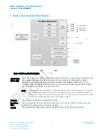
Figure 1: BT830 module block diagram
CS8811A08
(Main chip)
The BT830 is based on CSR8811A08 dual mode chip. The chip is a single-chip radio with on-chip
LDO regulators and baseband IC for Bluetooth 2.4 GHz systems including EDR to 3 Mbps.
Dedicated signal and baseband processing is included for full Bluetooth operation. The chip
provides PCM/I2S and UART interfaces. Up to four general purpose I/Os are available for general
use such as Wi-Fi coexistence or general indicators.
Note: The purpose of the SPI interface is to access the module’s inner settings such as selecting
different WLAN CO-EXIST scheme and enabling HID proxy mode. The SPI interface can
also be used to put the module in RF test mode. You cannot use the module over the SPI
interface for normal operation as the main host interface.
Antenna
The antenna is a ceramic monopole chip antenna.
Band Pass
Filter
The band pass filter filters the out-of-band emissions from the transmitter to meet the specific
regulations for type approvals of various countries.
Crystal
The embedded 26 MHz crystal is used for generating the clock for the entire module.

