background image

https://www.lairdconnect.com/wireless-

modules/bluetooth-modules 

34 

© Copyright 2019  Laird. All Rights Reserved 

Americas

: +1-800-492-2320 

Europe

: +44-1628-858-940 

Hong Kong

: +852 2923 0610 


A removable jumper (on J7 and J9) is provided to break the power supply line directly to the module, allowing you to measure 
current consumption. For normal operation, the jumper on J7 (and J9) must be fitted (and is fitted by default). 

IMPORTANT:


To achieve the optimal power consumption of the BL654PA series module on the development board, see 
the “

lp.low.power.deep.sleep.sb

” file in the GitHub 

smart

BASIC sample application repository on the 

BL654PA product page a

https://github.com/LairdCP/BL654PA-Applications


Note:  

This measures the current consumption of the 

BL654PA

 series module ONLY. 

The current drawn by the BL654PA series module can be monitored on the development board

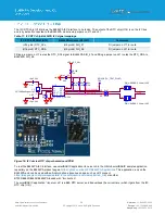
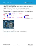
Figure 22

 shows the 

schematic and location of measuring points on the PCB related to current measurements.  


Figure 22: Current measurement schematic and PCB 

R79

10R,1%

SB13
NOPOP (Solderbridge)

1

1

2

2

PIN HEADER,2.54mm 1X2P

J9

1

1

2

2

VDD_HV

SB1
NOPOP (Solderbridge)

1

1

2

2

VDD_HVp

VDD_nRFp

SB2
NOPOP (Solderbridge_Open)

1

1

2

2

J7 jumper fitted (Default)

R76

10R,1%

PIN HEADER,2.54mm 1X2P

J7

1

1

2

2

VDD_nRF

J9 jumper fitted (Default)

SB12
NOPOP (Solderbridge_Open)

1

1

2

2

Summary of Contents for 455-00022

Page 1: ...Version 1 0 ...

Page 2: ...modules bluetooth modules 2 Copyright 2019 Laird All Rights Reserved Americas 1 800 492 2320 Europe 44 1628 858 940 Hong Kong 852 2923 0610 Version Date Notes Contributor s Approver 1 0 20 Aug 2019 Initial version Raj Khatri Jonathan Kaye ...

Page 3: ...4 6 3 SWD JTAG Interface 15 6 4 Four wire UART Serial Interface 17 6 5 UART Mapping 17 6 6 nAutoRUN Pin and Operating Modes 19 6 7 Virtual Serial Port Modes and Over the Air smartBASIC App Download 20 7 Software 21 8 Breakout Connector Pinouts 22 8 1 SIO Special Input Output Sockets Breakout Connectors 22 8 2 Additional Peripherals Sensors 26 8 2 1 Temperature Sensor 26 8 2 2 I2C Sensor RTC Chip 2...

Page 4: ... Board The development board has the required BL654PA module soldered onto it and exposes all available hardware interfaces Power Options USB cable Type A to micro type B The cable also provides serial communications via the FTDI USB RS232 converter chip on the board DC barrel plug for connection to external power supply 5 5 VDC max 3x AAA battery holder fitted on underside of development board Co...

Page 5: ...ith silkscreen AAA_5V5 Alternatively you have the option to inject external supply voltage anywhere between 3 0V to 5 5V BL654PA for the High Voltage mode via J28 pin1 and GND on J28pin2 J34 Coin cell holder and SW6 coin cell silkscreen coin cell position cannot be used for DVK BL664PA Since the BL654PA module is high power module coin cell CR2032 operation is not possible due to higher current dr...

Page 6: ...nsor via header in series no jumper by default I2C device RTC chip U16 via headers in series no jumper by default SPI device EEPROM QSPI device Flash IC via open solderbridges by default Four buttons and four LEDs for user interaction One reset button via an analog switch NFC antenna connector on board development board for use with supplied flexi PCB NFC antenna Optional external 32 768 kHz cryst...

Page 7: ...Y I2C device U16 SPI EEPROM device J41 PTH J47 PTH J29 PTH 4 Buttons NFC Antenna Connector CON2 Optional Serial QSPI flash SW3 nReset BOOT Button J48 PTH FTDI FT232R DC USB Power Source Switch SW4 Header J12 for nAutoRUN J35 J1 Header Plated Through Holes PTH for UART Temperatur e Sensor TP14 GND Hook LED2 LED1 LED3 LED 4 J37 J26 J45 J39 J5 VSP Optional 32 768 kHz Crystal On board SWD interface pr...

Page 8: ...ent board switches and jumpers must be configured as shown in Figure 3 Figure 3 Correct BL654PA DVK board 455 00022 or 455 00023 jumper and switch settings 455 00022 pictured SW7 middle position default for Normal Voltage VDD pin of BL654PA operation J12 Fit Jumper on Pins 2 1 SW5 default and ONLY position 3V3 SW6 default and ONLY position 3V3 1v8 SW11 position right default TP14 Black Test Hook S...

Page 9: ...default and only valid position is 3V3 SW5 position 1V8 is invalid DVK BL654PA SW6 default and only valid position is 3V3 1V8 SW6 position coin cell is invalid There are five options for powering the development board USB1 USB type micro B connector If it requires the FTDI USB1 UART BL654PA path USB2 USB type micro B connector If it requires the Atmel USB2 SWD BL654PA path USB3 USB type micro B co...

Page 10: ...d the VDD pin is not connected to any external voltage supply Connect external supply within a 3 0V to 5 5V range to the BL654PA VDD_HV pin Leave the BL654PA VDD pin unconnected For high voltage mode operation the BL654PA development board power supply section generates the following Regulated 2 5V SW8 position 2V5 cannot be used for BL654PA 3 x AAA generated 4 5V or inject external voltage into J...

Page 11: ...urce SW5 Note 2 Operating Mode Normal voltage Decided by SW5 default and only SW5 position is 3V3 N A N A SW7 bottom position Source SW8 Operating Mode High voltage Note 1 Decided by SW8 default and only SW8 position 5V5_AAA DVK BL654PA N A Power Source and Switch Location Notes Note 1 No voltage is presented to VDD pin as in High voltage mode the VDD pin becomes an output voltage pin It can be us...

Page 12: ...ce of VDD_nRF_SENSE is the BL654PA VDD pin When BL654PA is powered in High Voltage mode using the VDD_HV pin the BL654PA VDD pin becomes an output VDD_nRF_SW Selection switch SW6 supplies either VDD_SRC_nRF or coin cell J34 When the BL654PA operates in Normal Voltage mode SW7 in middle position and voltage source is either 1 8V or 3 3V selected by SW5 Also supplies the I2C RTC chip U16 The use cas...

Page 13: ... 1 INV IN1 2 Non INV IN1 3 VCC 4 Non INV IN2 5 INV IN2 6 OUT2 7 VCC 8 R137 1M U20 Load Switch IC 1A VOUT 1 GND 2 CONTROL 3 NC 4 VIN 5 VDD_nRF_SENSE R52 0R VDD_nRF_SENSE V5V Q2 DUAL NCH 20V 800mA S1 1 G1 2 D2 3 D1 6 G2 5 S2 4 GND VSUPPLY_EN R61 1M C18 0 1uF 16V GND GND GND GND Q3 NPN 45V 2 0A GND SB15 NOPOP Solderbridge_Open 1 1 2 2 VSUPPLY U21 Load Switch IC 1A VOUT 1 GND 2 CONTROL 3 NC 4 VIN 5 VD...

Page 14: ...ther the analog switch U25 control line USB_DETECT is low USB2 cable not plugged in or high USB2 cable plugged in the nReset button SW3 is routed via the analog switch U25 to BL654PA nReset pin nRESET_BLE The development board has USB2 cable detection circuit that generates the USB_DETECT signal on its output so if a USB cable is plugged into connector USB2 then USB2 cable detection circuit genera...

Page 15: ...K GND and VCC Firmware upgrades can still be performed over the BL654PA UART interface but this is slower 60 seconds using UART vs 10 seconds when using JTAG than using the BL654PA JTAG two wire interface Upgrading smartBASIC runtime engine firmware or loading smartBASIC applications also can be done using the UART interface For those customers using Nordic SDK that require access to BL654PA SWD J...

Page 16: ...XT JP1 pin4 OB_SWDIO SWDIO_BLE pin 1 SWDIO_EXT JP1 pin2 OB_RESET nRESET_BLE pin 19 via R131 0R Not populated nRESET_EXT JP1 pin10 OB_SWO SIO_32 pin 7 SWO_EXT JP1 pin6 via SB21 open solderbridge OB_SWDIO C80 0 1uF 16V GND OB_SWDCLK SB21 NOPOP Solderbridge_Open 1 1 2 2 USB_DETECTp VDD_VSRC_nRF USB_DETECTp Pins connect High 1A 1B1 2A 2B1 3A 3B1 4A 4B1 SWDIO_EXT SWDIO_BLE SIO_32_SWO_BLE nRESET_EXT R13...

Page 17: ... from Laird s UWTerminalX using the DTR tick box USB Connector The development kit provides a USB Type Micro B connector USB1 which allows connection to any USB host device The connector optionally supplies power to the development kit and the USB signals are connected to a USB to serial converter device FT232R when SW4 is set to the USB position USB UART The development kit is fitted with a U10 F...

Page 18: ... the BL654PA UART to be routed to Atmel MCU UART signal also on J19 and net names beginning with IMCU_ via open solder bridges SB16 to SB19 shown in Figure 13 You must connect these bridges with solder This may be useful for those customers wanting to work with the Nordic SDK IMCU_CTS IMCU_RxD C8 0 1uF 16V GND IMCU_RTS IMCU_TxD USB_CTS Module_CTS VDD_VSRC_nRF R7 10K R6 0R R9 0R R12 0R R21 0R USB_R...

Page 19: ...in28 nAutoRUN Mode SIO_35 Interactive Development Mode SIO_35 set High Externally Self contained Run Mode nAutoRUN mode SIO_35 Low Internally Circuit J12 Jumper Position Develop Jumper on J12 pins 2 1 nAutoRUN default Jumper on J12 pins 2 3 BL654PA has internal pull down enabled jumper in J12 in 2 3 can also be left off The J12 header connector allows the USB_DTR signal from the FTDI chip to be di...

Page 20: ... to be sent out of the BL654PA UART therefore data not stored on BL654PA VSP Command mode takes data sent from phone or tablet and sends it to the BL654PA This interprets as an AT command and the response is sent back The OTA Android or iOS application can be used to download any smartBASIC application script over the air to the BL654PA since a smartBASIC application is downloaded using AT command...

Page 21: ...clude the following Continually displayed status of DSR CTS DCD and RI Direct control of DTR on the host PC via a check box Direct control of RTS if CTS RTS Handshaking is disabled when UWTerminalX is launched Sending UART BREAK signals Following provides explanation UART Break https en wikipedia org wiki Universal_asynchronous_receiver transmitter Break_condition Additional built in features righ...

Page 22: ...tion script to change each SIO pin from the default function DIO UART to alternate functions AIN ADC I2C SPI QSPI DIO PWM FREQ and NFC The BL654PA development kit incorporates additional fly lead cables inside the box to enable simple hassle free testing of these multiple interfaces Table 8 shows the BL654PA module pins that are brought out to plated through Holes suitable for 2 54 mm pitch header...

Page 23: ... 54mm 1X2P J37 1 1 2 2 LED2 LED4 PIN HEADER 2 54mm 1X2P J39 1 1 2 2 PIN HEADER 2 54mm 1X2P J45 1 1 2 2 LED3 LED1 PIN HEADER 2 54mm 1X2P J26 1 1 2 2 SIO_15 SIO_14 SIO_13 SIO_16 PIN HEADER 2 54mm 1X2P J37 1 1 2 2 LED2 LED4 PIN HEADER 2 54mm 1X2P J39 1 1 2 2 PIN HEADER 2 54mm 1X2P J45 1 1 2 2 LED3 LED1 PIN HEADER 2 54mm 1X2P J26 1 1 2 2 SIO_15 SIO_14 SIO_13 SIO_16 PIN HEADER 2 54mm 1X2P J37 1 1 2 2 L...

Page 24: ...uted to Atmel Fit Jumper in J35 Jumper in J35 selects between BL654PA UART routed to FTDI Atmel MCU No Jumper on J35 default Routes SIO_05 RTS to FTDI CTS Routes SIO_06 TX to FTDI RX Routes SIO_07 CTS to FTDI RTS Routes SIO_08 RX to FTDI TX SIO_26 GND SIO_12 SIO_11 Eeprom_MISO_SIO_04 Eeprom_MOSI_SIO_40 Eeprom_SCK_SIO_41 SIO_30 SIO_27 J29 NOPOP PIN HEADER 2 54mm 1X10P 1 1 2 2 3 3 4 4 5 5 6 6 7 7 8 ...

Page 25: ...O_03 to Temp Sensor J6 pin 2 1 jumper NOT fitted default IMCU_CTS IMCU_RxD C8 0 1uF 16V GND IMCU_RTS IMCU_TxD USB_CTS Module_CTS VDD_VSRC_nRF R7 10K R6 0R R9 0R R12 0R R21 0R USB_RX R19 10K PIN HEADER 2 54mm 1X2P J35 1 1 2 2 USB_DETECT Pins connect High 1A 1B1 2A 2B1 3A 3B1 4A 4B1 Module_RX GND SIO_08 VDD_VSRC_nRF SIO_05 SIO_06 SIO_07 VDD_VSRC_nRF USB_TX USB_RTS VDD_VSRC_nRF U15 Dual DPDT 1 65V 4 ...

Page 26: ...W9 and Button4 SW10 the SIO pins direction and type must be set in the smartBASIC application to override the defaults in the BL654PA firmware For more information on these sample applications see GitHub smartBASIC sample applications repository on the BL654PA product page at https github com LairdCP BL654PA Applications The temperature sensor U1 by default is connected to the BL654PA module as ju...

Page 27: ...ble 9 Table 9 LM20BIM7 Specifications Output type Analogue output Accuracy at 30ºC 1 5ºC 4ºC max Accuracy at 40ºC to 85ºC approx 2 5ºC 5ºC max Power supply voltage range 2 4 V to 5 5 V Current Drain 10 uA max Output impedance 160 Ohms max The LM20BIM7 datasheet states the relationship of Temperature T to Voltage output Vo can be approximated as a linear equation for temperature range of 40ºC to 85...

Page 28: ...c and PCB To test the BL654PA I2C interface use smartBASIC application rtcs erver sb in the GitHub smartBASIC sample application repository on the BL654PA product page at https github com LairdCP BL654PA Applications This application runs on the BL654PA and can be used with an Android phone requires an app such as nRF connect https play google com store apps details id no nordicsemi android mcp hl...

Page 29: ...e using the SPI EEPROM U2 a smartBASIC application for this will be available in the future in the GitHub smartBASIC sample application repository on the BL654PA product page at https github com LairdCP BL654PA Applications The two push buttons and two LEDs on the BL654PA are connected to dedicated SIOs of the BL654PA module Table 13 LED s and Buttons to BL654PA SIO signal mappings Part BL654PA U5...

Page 30: ...pt example btn button led test sb in the GitHub smartBASIC sample application repository on the BL654PA product page at https github com LairdCP BL654PA Applications The LEDs are active high meaning that writing a logical one 1 to the output pin illuminates the LED One example of when push buttons can be used is when a smartBASIC application is written to simulate a generic data profile Push butto...

Page 31: ...A SIO signal mappings BL654PA U5 SIO Bring out SIO_9 and SIO_10 to NFC antenna connector CON2 Bring out SIO_9 and SIO_10 to Header connector J36 pin 59 NFC1 SIO_9 Fit R98 0R default Remove R100 0R default Remove R98 0R Fit R100 0R pin 57 NFC2 SIO_10 Fit R99 0R default Remove R101 0R default Remove R99 0R Fit R101 with 0R Figure 19 NFC antenna RF matching circuit NFC antenna connector schematic and...

Page 32: ...6 SIO_17 QSPI_CS Pin 1 CS SB7 BL654PA Dev board R126 10K pull up on therefore by default device not selected Drive from BL654PA line low to select Pin 14 SIO_19 QSPI_CLK Pin 6 SCLK SB4 Pin 13 SIO_20 QSPI_DIO0 Pin 5 SIO_0 SI SB5 Pin 12 SIO_21 QSPI_DIO1 Pin 2 SIO_1 SO SB6 Pin 11 SIO_22 QSPI_DIO2 Pin 3 SIO_2 WP SB11 Pin 9 SIO_23 QSPI_DIO3 Pin 7 SIO_3 HOLD SB10 The smartBASIC application for this exte...

Page 33: ... with radio power consumption in the system standby doze deep sleep modes by reducing the time that the Rx window must be open To connect the optional external 32 76kHz crystal oscillator circuit to the BL654PA module remove R127 and R128 and short SB8 and short SB9 Figure 21 Optional external 32 768kHz crystal circuit schematic and PCB A smartBASIC application will be available in the GitHub smar...

Page 34: ...the GitHub smartBASIC sample application repository on the BL654PA product page at https github com LairdCP BL654PA Applications Note This measures the current consumption of the BL654PA series module ONLY The current drawn by the BL654PA series module can be monitored on the development board Figure 22 shows the schematic and location of measuring points on the PCB related to current measurements...

Page 35: ...across J7 pins 1 2 can be used as current sense resistor Connect an oscilloscope or similar with two probes on the pins on the J7 connector and measure the differential voltage drop The voltage drop is proportional with current consumption If the 10 Ohm resistor is chosen 10 mV equals 1mA This method allows the dynamic current consumption waveforms to be shown on an oscilloscope as the BL654PA rad...

Page 36: ... infringement nor as to the fitness merchantability or sustainability of any Laird materials or products for any specific or general uses Laird Laird Technologies Inc or any of its affiliates or agents shall not be liable for incidental or consequential damages of any kind All Laird products are sold pursuant to the Laird Terms and Conditions of Sale in effect from time to time a copy of which wil...

Reviews: