L-Card ADC Series User Manual Download Page 31


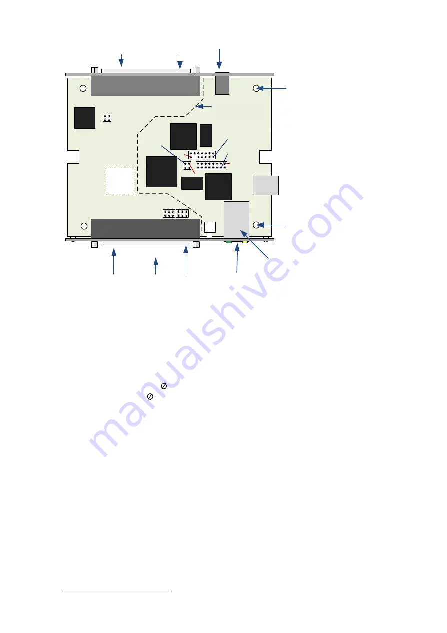
Fig. 4-2: The location of the "common wires" circuits on the E-502 board 

In particular, GND is a common wire for internal interfaces UART, JTAG Blackfin, JTAG 

ARM. 

If you use a separate E-502 board without a chassis

3

 in the embedded chassis circuit applications 

(CHASSIS), it is recommended to connect it to the solid metal surface of the chassis (case 
construction). Two right ports of 

3.05 mm on fig. 4-2 have a metal coating connected to a CHASSIS 

circuit, and two left ports of  3.05 mm are isolated from the other circuits. These 4 mounting ports 
are used to secure the E-502 board.   


4.4. E-502 connectors description 

4.4.1. Connector 

Analog

Connector Analog is a 37-pin 2-row type DRB-37M plug on the front panel of the E-502. The 

conductive connector contact piece (shield) is electrically connected to the GND signal ground 
circuit. On the shield of the cable part of the connector, the shield of the signal cable can be directly 
sealed. The connector 

Analog

 shield does not have a contact with AGND, DGND and other circuits 

of the 

Analog

 connector.        


3

 Here we do not consider the usage accuracy of the certified Measuring Device without a standard chassis. 

1

JTAG Blackfin 

(

GND

)

JTAG ARM

(

GND

)

1

1

UART

(

GND

)

ADSP-

BF523

FPGA

Cyclone

IV

SDRAM

SDRAM

ARM 

LPC4337

CPLD

USB

(

GND_USB

)

D I G I T A L

Элементы 

ЦАП

A N A L O G

Гальванический 

барьер

Отв

.    3,05 

мм

GHASSIS

Корпус 

разъёма

(

CHASSIS

Корпус 

разъёма

(

CHASSIS

Цифровые 

сигналы

(

DGND

DI_SYN1

(

DGND

A

налоговые  

сигналы

(

AGND

Изололированные 

входы 

Ethernet

GHASSIS

Отв

.    3,05 

мм

GHASSIS

0 V

DAC 

elements 

Digital signals 

Port Ø3,05 mm 

Port Ø3,05 mm 

Connector 

chassis 

Isolated Ethernet 

inputs 

Galvanic barrier 

Connector 

chassis 

Analog 

signals 

Summary of Contents for ADC Series

Page 1: ...IGN MANUFACTURING DISTRIBUTION http en lcard ru en lcard ru Revision 1 1 0 October 2017 E 502 P EU D I E 502 P EU D E 502 X EU X E 502 X U D E 502 X U X Measuring voltage converters A family of univer...

Page 2: ...vskoye shosse 5 block 4 bld 2 tel 7 495 785 95 19 fax 7 495 785 95 14 Internet contacts http en lcard ru E Mail Sales department en lcard ru Customer care en lcard ru E 502 Module Copyright 2014 2017...

Page 3: ...0 6 The operating temperature range in the table of section 5 9 has been brought into correspondence amended the section 5 8 the tables in subparagraphs 1 1 1 are amended 2 1 02 2017 1 0 7 Paragraph...

Page 4: ...5 Serial number E 502 version number Module identification in a multi module configuration 15 2 6 E 502 application as a part of user programs 15 2 7 Software installation 15 2 8 Ethernet interface co...

Page 5: ...t settings of the input of the ADC E 502 43 4 7 1 The physical causes of possible problems 43 4 7 2 Conditions for correct E 502 connection and settings 43 4 8 Calculation of total load power of E 502...

Page 6: ...7 Connecting a power supply to the ADC input 59 6 1 8 The coordinated connection of remote sources of current or voltage through a long line with a wave impedance Zw 61 6 1 9 The coordinated connectio...

Page 7: ...output 5 V asynchronous or synchronous mode with a conversion frequency of up to 1 MHz for each channel Digital input up to 17 digital inputs of general purpose asynchronous or synchronous data output...

Page 8: ...E 502 module for the order it should be noted that when you contact the L Card sales department the previously purchased E 502 module can not be modified to another modification or design version Inf...

Page 9: ...cs For DB 37 connectors DJK 10A straight connector 1 pc 1 pc 1 pc To connect low voltage power from a non standard power source Cable Ethernet Pathcord 5e L 1 5 m 1 pc USB cable type A B L 1 8 m 1 pc...

Page 10: ...1 2 Appearance and main structural elements Fig 1 2 Front view front panel Fig 1 3 Back view back panel...

Page 11: ...n fig 2 1 on the left Programmed control no jumper on fig 2 1 on the left Programmed control no jumper on fig 2 1 on the left Output setting DAC1 15V AGND NC on Analog connector DAC1 See fig 2 1 DAC1...

Page 12: ...ws and disassemble the housing covers Reassemble in the reverse order DAC1 15V AGND DAC1 15V AGND DAC2 15V GNDD DAC2 15V AGND 1 JTAG Blackfin JTAG ARM 1 1 UART ADSP BF523 FPGA Cyclone IV SDRAM SDRAM A...

Page 13: ...ility of programmed transfer to the third state in this case you need to install one or two additional jumpers according to fig 2 1 This setting is made when the initial high impedance state of the di...

Page 14: ...be either a sign of E 502 failure or a sign of the heavy external electromagnetic environment in which the E 502 is located which led to a malfunction Contact the L Card technical support if the E 502...

Page 15: ...mention in the documentation for his system the E 502 module of the L Card production as the component part the completing unit 2 7 Software installation To install the necessary drivers and libraries...

Page 16: ...to have their own low level programming of the processor possibly with the use of the JTAG emulator s 4 4 3 p 39 All E 502 modifications have a galvanic isolation of the signal circuits for L 502 a ga...

Page 17: ...r in the Blackfin processor E 502 has a mechanism of the intermodule synchronization s 3 3 5 p 20 to form a single synchronous I O system E 502 has a 32 bit data word format in the format of which bes...

Page 18: ...and the size of the control table n can be set from 1 to 256 In each cell of the control table the physical number of the ADC polling channel is prescribed Within the frame the control table will be...

Page 19: ...other channels assigned as synchronous the same synchronous mode is supported either a streaming or an self oscillator from an internal buffer 3 3 4 1 Restrictions on the current implementation of asy...

Page 20: ...as the master We list all possible options for user settings for selecting sources of the start event of the E 502 I O system Program start from PC default setting On the signal from the input DI_SYN...

Page 21: ...ation signal are supported Enable of ADC data on the edge drop of an analog or digital signal Enable of ADC data at a level above the threshold or below the threshold for analog synchronization or at...

Page 22: ...it But if it is required to use the E 502 at a data acquisition rate for each channel less than the maximum and it is possible to reduce the switching frequency then in E 502 with internal synchroniza...

Page 23: ...he high frequency components of the spectrum above the Nyquist frequency of 0 5 fch for a given physical channel associated with one or more logical channel Note in passing that digital filtering by t...

Page 24: ...tsw between neighboring channels of one frame and equal tsw td between the nearest channels of neighboring frames separated by interframe delay If the averaging mode is used nav 1 where nav are assig...

Page 25: ...500 ns 2 MHz 667 ns 1 5 MHz Duration of the signal pulse CONV_OUT tW 50 ns Group delay time of analog channel of ADC channel in E 502 tADC_SU 15 70 ns The delay time from the front CONV_OUT to the sa...

Page 26: ...n tST_H 150 ns The time to set the data at the DI input tDI_SU 5 ns Data hold time at the DI input tDI_H 1 ns DO delay time relative to the front CONV_OUT tDO 6 ns The group delay time of the signal a...

Page 27: ...02 modification All E 502 modifications have a LPC4333 LPC4337 ARM controller and a galvanic isolation ARM LPC4333 4337 HOST DMA ADSP BF523 E 502 FPGA Cyclone IV JTAG X1 X16 Y1 Y16 GND32 DI_SYN1 DI_SY...

Page 28: ...turned on the error is indicated by LED2 s 2 3 2 p 14 Processors LPC4333 LPC4337 are identical in terms of their resources involved and the option of bundling does not affect the consumer properties...

Page 29: ...xternal synchronization DI_SYN2 Is present separately on the internal connector L 502 Programmable pull up resistor of DI_SYN2 input Is combined with D14 input Programmable pull up resistor of DI14 DI...

Page 30: ...dule in the non isolated part 0 V is a circuit of the zero potential of the low voltage E 502 power input GND_USB is a common wire circuit of USB interface CHASSIS is a circuit for chassis connection...

Page 31: ...row type DRB 37M plug on the front panel of the E 502 The conductive connector contact piece shield is electrically connected to the GND signal ground circuit On the shield of the cable part of the c...

Page 32: ...el voltage input 1 16 for differential mode Input channels 17 32 for the mode with common ground Operation voltage range 10 V see the details in section 4 6 p 41 Unused inputs X 1 16 are recommended t...

Page 33: ...In the with common ground mode common inverting channel input 1 32 For all modes must be connected to AGND in differential mode to increase noise immunity In the with common ground mode the connectio...

Page 34: ...gnal cable can be directly sealed The Digital connector shield has no contact with the DGND circuits and the remaining circuits of the Digital connector Fig 4 4 Connector Digital 1 20 2 3 4 5 6 7 8 9...

Page 35: ...h the E 502 power off The input is compatible with the output logic level of the TTL CMOS cells with a supply voltage of 2 5 V to 5 V There is a Schmitt trigger at this input DI16 START_IN DGND Input...

Page 36: ...ut Output 3 3 V Output 3 3 V supply external digital nodes Short circuit of the 3 3 V circuit is undesirable but permissible causes heat protection of the internal stabilizer For the maximum permissib...

Page 37: ...ow logic level on the last slave module in the circuit It is recommended that no more than 2 adjacent slaves are connected to the same chain with the master Each slave in the circuit for example E 502...

Page 38: ...ows an almost important case of implementing interfaces with various devices that have an 8 bit bidirectional data bus input and output control lines It should be noted that DI14 DI15 DI16 inputs have...

Page 39: ...To debug your own Blackfin software on the board you probably will not need to modify the ARM controller software that performs the interface function E 502 However for advanced users such a modifica...

Page 40: ...it Digital inputs of dual purpose DI14 DI_SYN2 DI15 ONV_IN DI16 START_IN From 0 4 to 3 6 V relative to DGND circuit DO digital outputs From 0 4 to 3 6 V relative to the DGND circuit the current is not...

Page 41: ...GND are indicated In the first two circuits the voltage UYi UYj should not exceed 1 V in order to ensure the operating mode and in the latter scheme the common mode voltage UXi UYi 2 must be within 1...

Page 42: ...E 502 Z1 UYi GND E 502 Z UYi GND32 X Y i i L 502 X Y j j GND2 GND1 Z2 X j Y j GND1 UYj L 502 L 502 X i Y i GND E 502 U GND Z UYi UXi Differential VS and differential mode L 502 Remote single phase VS...

Page 43: ...itch when tuned to multi channel mode with E 502 default settings may not only be a big advantage of the ADC E 502 in the high speed ADC input interrogation but it can also be a problem because of the...

Page 44: ...le averaging factor nav 1 s 3 3 6 for the required channel polling frequency and the necessary signal conditioning time nsu 11 Do not exceed the operating voltage ranges at the inputs X Y GND32 s 4 6...

Page 45: ...st be calculated either through the known load current by the formula or through the known load resistance at the i th output The power summands of the corresponding j th outputs must be calculated ei...

Page 46: ...ntial measurement mode on the subbands 10 V 5 V The average value of the voltage at the inputs X and Y for the differential mode on the measurement subranges 2 V 1 V 0 5 V 0 2 V Voltages at the GND32...

Page 47: ...cl 1 02 0 3 0 X X AC more than 100 to 300 incl 1 03 0 1 X X AC more than 300 to 999 1 05 0 5 X X AC Notes 1 The error in measuring the AC voltage is normalized in the differential connection scheme E...

Page 48: ...ends on many factors of the software and hardware environment DAC bit depth bit 16 Output modes Asynchronous Synchronous streaming synchronous self oscillator Output signal range 5 V Operating range o...

Page 49: ...resistors activation for inputs DI1 DI16 No pull up resistors unlike L 502 for inputs DI_SYN1 DI_SYN2 Regardless of each input Maximum speed in synchronous mode 2 Mwords s Maximum speed in asynchronou...

Page 50: ...cal zero max 2 4 V logical unit Output logic elements with a supply voltage of 3 3 V Output resistance typical value 110 Ohm Maximum leakage current in operating mode in high impedance state 1 A High...

Page 51: ...t via Ethernet on output 5 Mwords s 2 5 Mwords s To be confirmed Interfaces of ADSP BF523 E 502 P signal processor Interface with a computer HOST DMA 16 bits Main interface of input output for ADC DAC...

Page 52: ...ly isolated circuits 10 kV s The method for estimating the load power is given in p 4 8 p 44 The total load power taken from all outputs E 502 according to the method of estimating the load power is g...

Page 53: ...under climatic influences the converters in addition to the versions with the letter index I correspond to GOST 22261 group 3 with an extended range of operating temperatures environment temperature f...

Page 54: ...not cover all the features of the connection for your particular case If necessary please contact en lcard ru or in the conference on the site en lcard ru 6 1 ADC entry point connection 6 1 1 Connecti...

Page 55: ...t of the voltage in the frequency band is R2 R1 R2 If multichannel mode it is necessary that 1 FADC R1 R2 C 10 10 R1 R2 or if R2 is not present then 1 FADC R1 C 10 10 R1 where FADC is the ADC conversi...

Page 56: ...t be connected like this 6 1 1 11 Inductive pickup Mode with common ground 6 1 1 12 Inductive pickup Differential mode Resistor R performs the function of a damper to suppress the oscillation process...

Page 57: ...502 input Only for voltage subbands 2 V 1 V 0 5 V 0 2 V It is necessary R1 50 if the switching frequency is maximal R1 R2 R3 R4 Locate R1 R2 close to E 502 input The voltage transfer ratio is R1 R2 R1...

Page 58: ...ion 4 6 p 412 6 1 4 Measurement of the voltage drop on the circuit section in the differential mode up to 16 channels This connection allows you to measure the voltage drop across resistor R2 For a si...

Page 59: ...ADC input 6 1 7 1 Mode with common ground 6 1 7 2 Differential mode Fixed ADC U subband must correspond to U IMAX R and the current source must have a voltage margin of at least U Resistor R should a...

Page 60: ...V 0 2 V Fixed ADC U measurement subband must correspond to U IMAX R while the current source must have a voltage margin of at least U Resistor R should always be located close to the ADC input Resisto...

Page 61: ...y matching of the long line on the side of the signal receiver 6 1 8 1 Mode with common ground 6 1 8 2 Differential mode 6 1 8 3 Differential connection of an isolated current source or voltage R1 R2...

Page 62: ...tor on the signal source side The cable must be paired shielded twisted pairs with wave resistance of wire pairs Zw Below is a practical case where a broadband operational amplifier acts as a remote v...

Page 63: ...preconfigured with jumper see p 2 2 1 p 13 6 2 1 Mode with common ground 2 channel output 5 V 6 2 2 Single channel differential output 10 V The differential output 10 V is realized as a difference vo...

Page 64: ...act The recommended resistor R1 nominal is from 3 to 5 kOhm The open contact corresponds to a logical zero The recommended resistor R1 nominal is from 3 to 5 kOhm 6 3 4 Connect the optron output to th...

Page 65: ...Chapter 7 Design data 7 1 Circuit plate draft Note diameter of 4 ports taking into account metallization 3 05 mm 4 ports of 3 2...

Page 66: ...7 2 Front panel draft 7 3 Back panel draft 2 ports of 5 5...

Page 67: ...tables Table 4 1 Connector Analog 32 Table 4 2 Connector Digital 35 Table 4 3 Maximum permissible E 502 input output conditions 40 Table 4 4 Maximum permissible through currents by common wires circu...

Page 68: ...ous I O diagram 25 Fig 3 5 Block diagram 27 Fig 4 1 Internal connection of the common wires circuits in E 502 30 Fig 4 2 The location of the common wires circuits on the E 502 board 31 Fig 4 3 Connect...

Page 69: ......

Reviews: