KTD-S0031-E
Page 29
Power Supply
KTA55/pITX
User's Guide
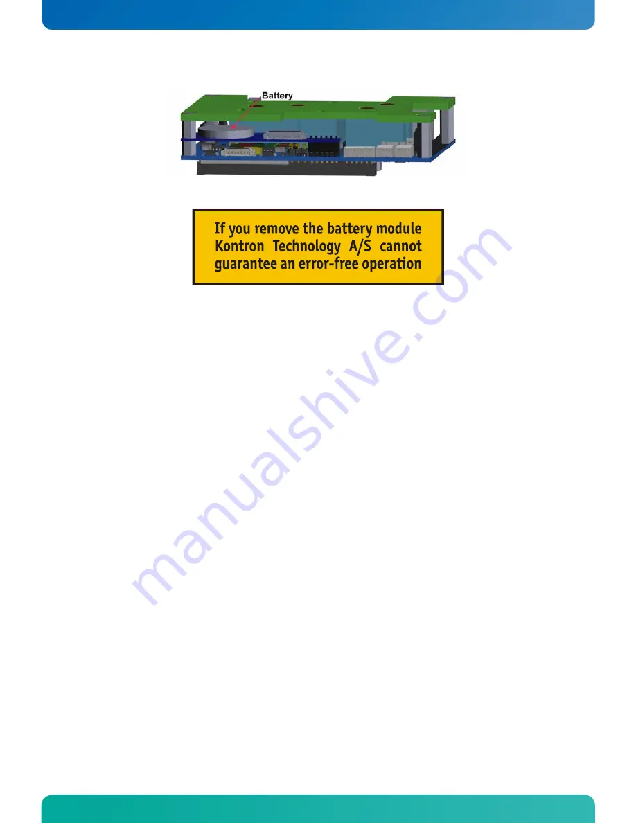
When the board is shipped the RTC battery is mounted on the RTC battery module.
Page 1: ...KTA55 pITX KTD S0031 E...
Page 2: ...pecifications 8 3 4 Electrical Specifications 8 3 5 Real Time Clock Battery 9 3 6 Environmental Specifications 9 3 7 MTBF 10 4 Getting Started 11 5 System Memory 11 6 Graphics Interface 12 6 1 DVI I C...
Page 3: ...4 13 LPC Bus 25 13 1 Connector 25 14 Power Supply 26 14 1 Connector 26 14 2 External Power Connector Alternative 26 14 3 Power Front Panel Header 27 14 3 1 Power and Harddisk LED 27 14 4 Onboard Statu...
Page 4: ...5 5 Miscellaneous Submenu 42 18 5 5 1 Cooling Monitor Submenu 42 18 5 5 2 Active Cooling Configuration Submenu 43 18 5 5 2 1 Enhanced Fan Control Submenu 44 18 6 Trusted Computing Menu 44 18 7 Boot Me...
Page 5: ...ically for any purpose without the express written permission of KONTRON Technology A S 1 3 Trademarks Brand and product names are trademarks or registered trademarks of their respective owners 1 4 St...
Page 6: ...can be reasonably expected to cause the failure of the life support device or system or to affect its safety or effectiveness 1 7 Technical Support Please consult our web site at http www kontron com...
Page 7: ...terized by the same front line pinouts and interfaces for reset logic and simple power supply 2 x USB Gigabit LAN S ATA Audio GPIOs DVI and LVDS interface These embed ded line family features allow to...
Page 8: ...used as GPIOs S Sixteen USB channels OHCI EHCI only six channels available S Six S ATA ports only two ports available S Integrated High Definition audio with four streams HD audio only one stream use...
Page 9: ...PHONE IN and S PDIF output S Unified Audio Architecture UAA compatible Onchip Digital I O S Eight bidirectional I O lines 3 3V signal level Onchip Temperature Monitoring S One CPU and one chipset temp...
Page 10: ...0031 E Page 6 Specifications KTA55 pITX User s Guide Watchdog Timer CPLD S Seven discrete time out values from 1 second to 10 minutes BIOS AMI 4 MB Flash BIOS Real Time Clock RTC with CMOS RAM and bat...
Page 11: ...pITX USB Controller S ATA Controller HD Audio Controller GPIOs PCI Express Ports SDRAM Controller S ATA 0 1_ J1801 J1802 J1803 USB 0 5_ Ethernet Intel 82574L J1804 J2200 J2201 DisplayPort to LVDS CH75...
Page 12: ...executed during the DOS prompt with 4 GB DDR3 SDRAM DVI monitor USB keyboard and S ATA SSD Solid State Drive external powered as boot device default BIOS settings Full Load Soft Off S5 A W A W 2 85 14...
Page 13: ...nte Disponga las bater as usadas seg n las instrucciones del fabricante ADVARSEL Lithiumbatteri Eksplosionsfare ved fejlagtig h ndtering Udskiftning m kun ske med batteri af samme fabrikat og type Lev...
Page 14: ...s data when used is specified at 50 C so in that sense the following results are slightly conservative The MTBF values shown below are for a 40 C in an office or telecommunications environment Higher...
Page 15: ...tostart jumper J2403 Enter the BIOS by pressing the Del key during boot up Make all changes in the BIOS Setup See the BIOS Setup chapter of this manual for details 5 System Memory The KTA55 pITX uses...
Page 16: ...MDS1 TMDS data 1 negative 10 TMDS1 TMDS data 1 positive 11 GND Ground 12 N C Not connected 13 N C Not connected 14 VCC 1 Power 5V 15 GND Ground 16 TMDS_HPD Hot plug detect 17 TMDS0 TMDS data 0 negativ...
Page 17: ...utput 1 positive 5 FTX2 First channel data output 2 negative 6 FTX2 First channel data output 2 positive 7 GND Ground 8 FTXC First channel clock output negative 9 FTXC First channel clock output posit...
Page 18: ...s easy Check whether you have the correct adapter and cable for the panel you plan to use Inspect the cable for damages Disconnect the power from your system Check jumper J1203 for correct panel volta...
Page 19: ...c 640 x 200 2 07h Text 80 x 25 2 0Dh Graphic 320 x 200 16 0Eh Graphic 640 x 200 16 0Fh Graphic 640 x 350 2 10h Graphic 640 x 350 4 11h Graphic 640 x 480 2 12h Graphic 640 x 480 16 13h Graphic 320 x 20...
Page 20: ...the power connector J2901 This connector can also be used to power the board with 5V DC instead of the round power jacket see chapter Power Supply Note The backlight voltage that is sourced through c...
Page 21: ...ff Note 1 To protect the external power lines of peripheral devices make sure that the wires have the right diameter to withstand the maximum available current the enclosure of the peripheral device f...
Page 22: ...r USB ports are available through the extension connectors J1802 J1803 and J1805 J1806 4 pins To have the signals available on the standard USB interface connectors an adapter cable is required An USB...
Page 23: ...parallel interface requiring 40 separate wires to a serial interface requiring only 6 wires 8 1 Connector The S ATA interface is available through the standard L type connectors J1500 and J1501 7 pins...
Page 24: ...the BIOS Setup to allow the system to boot up via a network connection from a PXE server 9 1 Connector The LAN interface is available through the standard RJ45 connector J1900 8 pins Header Pin Signa...
Page 25: ...INE OUT S PDIF 44 1 48 96 192 kHz Output signal to noise ratio LINE OUT 97 dB Output current S PDIF 12 75 mA Input resolution LINE IN 16 20 bit Input sample rate LINE IN 44 1 48 96 kHz Input signal to...
Page 26: ...ts one or four bits the SDIO transfer rate can be up to 50 MHz 11 1 microSD Card Connector The microSD card socket is named J2000 8 pins Header Pin Signal Name Function 1 DAT2 Data bit 2 2 CD DAT3 Car...
Page 27: ...access 1 6 MHz 12 2 Connector The digital I O interface is available through the connector J1804 10 pins Header Pin Signal Name Function 1 VCC 1 Power 3 3V 2 GPIO4 Bidirectional I O 4 3 GPIO0 Bidirec...
Page 28: ...art number 62038 Header Pin Signal Name Function 1 VCC 1 Power 3 3V 2 GPIO4 Bidirectional I O 4 3 GPIO0 Bidirectional I O 0 4 GPIO5 Bidirectional I O 5 5 GPIO1 Bidirectional I O 1 6 GPIO6 Bidirectiona...
Page 29: ...voltages above 3 3V LPC bus signals are unprotected against overvoltage 13 1 Connector The LPC bus interface is available through the connector J1800 10 pins Header Pin Signal Name Function 1 VCC 1 Po...
Page 30: ...I O connector The maximum current should not exceed 250mA 14 2 External Power Connector Alternative This connector can also be used to power the board with 5V DC instead of the round power jacket The...
Page 31: ...Power button positive 3 RST_BTN Reset button negative 4 PWR_BTN Power button negative 5 RECOVERY Recovery pin 6 RSVD Reserved 7 PWR_LED Power LED negative 8 HDD_LED Harddisk LED negative 9 PWR_LED Pow...
Page 32: ...2 pins Header Pin Signal Name Function 1 VBAT 1 Battery input voltage 3V 1 2 2 GND Ground Note 1 To protect the external power lines of peripheral devices make sure that the wires have the right diam...
Page 33: ...KTD S0031 E Page 29 Power Supply KTA55 pITX User s Guide When the board is shipped the RTC battery is mounted on the RTC battery module...
Page 34: ...on J2402 Power up the board and enter the BIOS Setup Remove the jumper on J2402 Saving your settings with Save Changes and Exit The board should be functional now 15 2 Restore Failed BIOS Update Take...
Page 35: ...Page 31 Autostart Function KTA55 pITX User s Guide 16 Autostart Function When the KTA55 pITX should start directly when the power is applied without a power button signal the autostart jumper J2403 m...
Page 36: ...on the KTA55 pITX The optimum cooling solution varies depending on the application and environmental conditions Attention After the heat sink has been mounted it cannot be removed anymore because aft...
Page 37: ...which allows the control of fan speed 17 3 1 Connector The fan interface is available through connector J1503 Header Pin Signal Name Function 1 SENSE Speed monitoring 2 VCC 1 Power 5V 3 GND Ground Not...
Page 38: ...tion Bios Information BIOS Version IP55R Build Date 18 2 Start AMI BIOS Setup Utility To start the AMI BIOS Setup utility press DEL when the following string appears during boot up Press DEL to run Se...
Page 39: ...es F4 Save and exit Enter Execute command or select submenu Selecting an Item Use the or key to move the cursor to the field you want Then use the and keys to select a value for that field Displaying...
Page 40: ...d Information Submenu Show additional service information Time HH MM SS Set the system time Date MM DD YYYY Set the system date 18 4 1 Board Information Submenu Feature Option Description Product Name...
Page 41: ...cache size L2 Cache N A Display the L2 cache size Execute Disable Bit Capability Disabled Enabled This option can help to prevent certain classes of buffer overflow errors AMD NX bit or Intel XD bit...
Page 42: ...mory detected during boot up Memory Clock Auto DDR800 DDR1066 This option allows to select a different memory clock Memory Clear Disabled Enabled Memory clear functionality I O Memory Mapping Unit Dis...
Page 43: ...torage device emulation type 18 5 2 4 Audio Configuration Submenu Feature Option Description HD Audio Controller Disabled Enabled Auto Enable or disable the HD audio controller Azalia 18 5 2 5 LAN Con...
Page 44: ...ntroller port 5 USB 2 0 Controller Port 0 4 Disabled Enabled Enable or disable the USB 2 0 EHCI functionality Port 0 4 USB 2 0 Controller Port 5 Disabled Enabled Enable or disable the USB 2 0 EHCI fun...
Page 45: ...from hub descriptor Device Power Up Delay 1 Sec 5 Sec 40 Sec Define the device power up delay Device Emulation Type Auto Floppy Forced FDD Harddisk DVD ROM Define the emulation type Forced FDD can be...
Page 46: ...nvoke the VGA BIOS post on suspend event resume USB Wakeup from S3 S4 Disabled Enabled Enable or disable USB wake event S5 Behaviour Disabled Enabled Allow board to enter S5 Watchdog Timeout Disabled...
Page 47: ...21 48 kHz 19 83 kHz 18 41 kHz 100 Hz 87 Hz 58 Hz 44 Hz 35 Hz 29 Hz 22 Hz 14 Hz 11 Hz Select the fan frequency PWM Step Rate 0 1 100 Define the Pulse Width Modulation PWM step rate Temperature Sensor C...
Page 48: ...Temp 5 Threshold 0 C 100 C Define temperature 5 threshold PWM 5 Percentage 0 100 Define PWM 5 percentage Temp 6 Threshold 0 C 100 C Define temperature 6 threshold PWM 6 Percentage 0 100 Define PWM 6...
Page 49: ...ired to launch active boot option Skip VGA Disabled Enabled If enabled BIOS will skip the EFI VGA driver Skip USB Disabled Enabled If enabled USB devices will not be available until after OS boot Setu...
Page 50: ...ou may have made Save Changes and Reset Yes No Reset the system after saving the changes Discard Changes and Reset Yes No Reset system setup without saving any changes Save Changes Yes No Save changes...
Page 51: ...only valid in legacy mode e g DOS most operating systems are using the APIC assignment Legacy mode IRQ Used for Available Comment 0 Timer 0 No 1 Keyboard No 2 8259 Slave Cascade No 3 Yes 4 PCI IRQ for...
Page 52: ...lave Cascade No 3 Yes 4 Yes 5 Yes 6 Yes 7 Yes 8 Real Time Clock RTC No 9 ACPI Power Management No 10 Yes 11 Yes 12 Yes 13 Floating Point Unit FPU No 14 S ATA Legacy IDE Yes Note 1 15 S ATA Legacy IDE...
Page 53: ...sed for Available Comment 0170h 0177h S ATA Controller Legacy Mode Yes Chipset Note 2 01F0h 01F7h S ATA Controller Legacy Mode Yes Chipset Note 2 0376h S ATA Controller Legacy Mode Yes Chipset Note 2...
Page 54: ...t ATI SMBus Controller Chipset ATI S ATA Controller Chipset ATI Audio Azalia Controller Chipset ATI LPC Bus Controller Chipset ATI PCI Bridge Chipset ATI USB 1 1 Controller Chipset ATI USB 1 1 Control...
Page 55: ...for external SMBusTM devices SMBus 0 SMBusTM Address Device Comment A0h A1h SPD Eeprom DDR3 SDRAM Read only SMBus 1 SMBusTM Address Device Comment 42h 43h Chrontel DisplayPort LVDS Controller SMBus 2...
Page 56: ...KTD S0031 E Page 52 Appendix B Connector Layout KTA55 pITX User s Guide Appendix B Connector Layout B 1 Connector Locations B 1 1 Top Side...
Page 57: ...KTD S0031 E Page 53 Appendix B Connector Layout KTA55 pITX User s Guide B 1 2 Bottom Side B 1 3 Battery Module J2 J1 Digital I O Battery...
Page 58: ...KTD S0031 E Page 54 Appendix B Connector Layout KTA55 pITX User s Guide B 2 Mechanical Dimensions...
Page 59: ...omp for fan interface J1800 1 25 mm 10 pin MOLEX 51021 1000 or comp for LPC interface J1802 J1803 J1805 J1806 1 25 mm 4 pin MOLEX 51021 0400 or comp for USB adapter J2200 1 25 mm 2 pin MOLEX 51021 020...
Page 60: ...C FTX1 VDD 5 N C FTX2 VDD 6 DDC_CLK FTX2 GND 7 DDC_DATA GND BKLTON 8 VSYNC FTXC 9 TMDS1 FTXC 10 TMDS1 FTX3 11 GND FTX3 12 N C STX0 13 N C STX0 14 VCC5 GND 15 GND STX1 16 TMDS_HPD STX1 17 TMDS0 GND 18...
Page 61: ...Standard J1801 USB Extension J1802 J1806 1 TXD BI_D1 VCC5 GND 2 TXD BI_D1 USB0 USBn 3 RXD BI_D2 USB0 USBn 4 BI_D3 GND VCC5 5 BI_D3 VCC5 6 RXD BI_D2 USB1 7 BI_D4 USB1 8 BI_D4 GND Pin S ATA J1500 01 HD...
Page 62: ...a io org developers IEEE 802 3 Specification Ethernet http standards ieee org getieee802 Low Pin Count Interface Specification LPC Bus http developer intel com design chipsets industry lpc htm Open LV...
Page 63: ...KTD S0031 E Page 59 Appendix D Certifications KTA55 pITX User s Guide Appendix D Certifications...
Page 64: ...KTD S0031 E Page 60 Appendix D Certifications KTA55 pITX User s Guide...
Page 65: ...KTD S0031 E Page 61 Appendix D Certifications KTA55 pITX User s Guide...
Page 66: ...KTD S0031 E Page 62 Appendix D Certifications KTA55 pITX User s Guide...
Page 67: ...subchapter Simultaneous Mode and some interface cable part numbers S0031 A 12 14 11 MHU Added and changed some table contents and Bios Setup entries e g chapter 18 5 4 18 6 and App A1 A3 and A4 S0031...