


18
Keysight M8132A 640 GSa/s Digital Signal Processor User’s Guide
1
Introduction
Instrument Options
The M8132A can be ordered as M8132A-002. The -002 indicates that two
Xilinx Ult VU9P FPGAs are available.
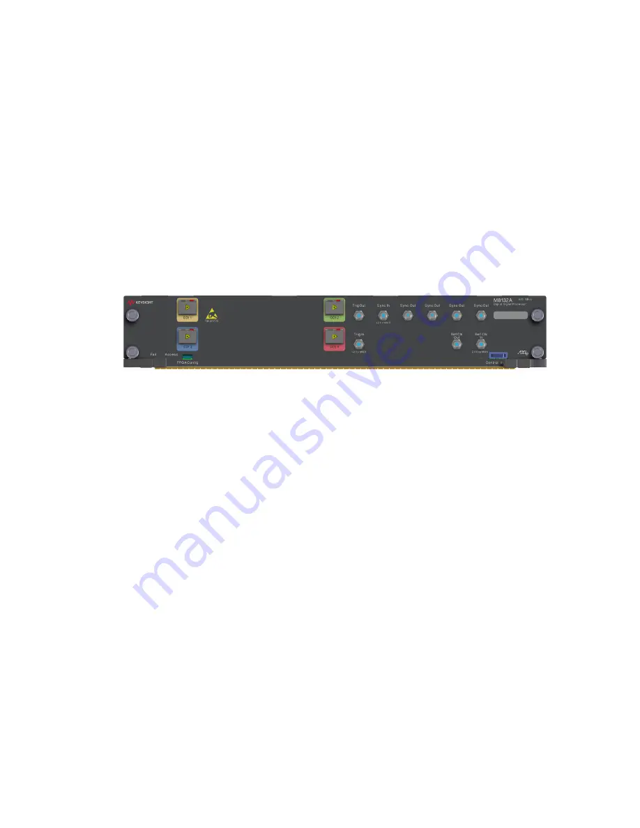
Front Panel
on page 18 illustrates the front panel of the M8132A instrument.
Figure 1
M8132A front panel
The M8132A front panel includes the following input/output ports:
Inputs/Outputs
•
ODI
- The four Optical Data Interface ports (ODI 1/2/3/4) can be used
for optical data streaming.
•
Trig In
- The Trigger Input can be used for external triggering. As
Trigger source e.g. an external pulse generator can be connected. The
FPGA designer has access to the “Trigger Input” signal inside both
FPGA and may implement desired functionality. The Trigger Input
functionality is for future use and is currently not available.
•
Trig Out
- The Trigger Output can be used to trigger external
instruments or DUTs. The FPGA designer can control the “Trigger
Output” signal inside both FPGA and may implement desired
functionality Trigger Output functionality is for future use and is
currently not available.
•
Sync In
- The Sync Input can be used to synchronize the M8132A DSP
module with an M8131A digitizer module in order to achieve a
deterministic latency between the M8131A and the M8132A. Sync In
of the M8132A is connected to the Sync Out of the M8131A digitizer
module.