background image

TKR-740

13

REALIGNMENT

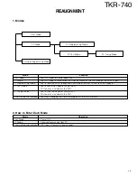
1. M odes

User Mode

Firmware Programming Mode

PC Programming Mode

PC Test Mode

PC Tuning Mode

PC Mode

M ode

User Mode
PC Mode
PC Programming Mode
PC Test Mode

PC Tuning Mode

Firmware Programming Mode

Function

Use this mode for normal operation.
Use this mode to make various settings by means of the FPU through the RS-232C port.
Use to read and write frequency data and other features to and from the Repeater.
Use to check the Repeater using the PC.
This feature is included in the FPU.
Use to tune the Repeater using the PC.
This feature is included in the FPU.
Use when changing the Firmware program of the flash memory.

M ode

User Mode
PC Mode
Firmware Programming Mode

Operation

Power ON.
Received commands from PC.
[PF1] key + Power ON (one second).

2. How  to Enter Each M ode

Summary of Contents for TKR-740

Page 1: ...ADJUSTMENT 69 PC BOARD CONTROL UNIT X53 3882 71 81 TX UNIT X56 3072 70 91 RX UNIT X55 3050 11 103 SCHEMATIC DIAGRAM 109 BLOCK DIAGRAM 121 LEVEL DIAGRAM 123 INTERCONNECTION DIAGRAM 125 KES 4 EXTERNAL SPEAKER 127 KPG 46 PROGRAMMING INTERFACE CABLE 128 SPECIFICATIONS BACK COVER TKR 740 2002 12 PRINTED IN JAPAN B51 8642 00 S 272 LED B30 2197 05 PUSH KNOB TEST K29 3002 14 MODULAR JACK E08 0876 05 LED B...

Page 2: ...er Service Bulletins or Manual Revisions These are issued as required ORDERING REPLACEMENT PARTS When ordering replacement parts or equipment information the full part identification number should be included This applies to all parts components kits or chassis If the part number is not known include the chassis or kit number of which it is a part and a sufficient description of the required compo...

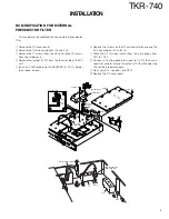
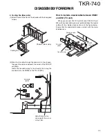
Page 3: ...r the 5 leads in place 6 Replace the screws on the RX unit and shield case and the flat clip spring on IC4 and L16 7 Move the RX IN signal cable from the back panel from CN1 to CN10 8 Connect a tracking generator signal to RX IN then use a spectrum analyzer to read the output at CN2 while adjusting L16 for the proper response 9 Next adjust IF squelch and RSSI 0 Replace the RX cover panel RX UNIT P...

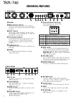
Page 4: ...lity external frequency reference oscillator 10MHz 10dBm or higher to this BNC receptacle optional yyyyy DC 13 2V jack Connect a 13 2 V DC power supply to this jack uuuuu FUSE Insert a 10 A blade fuse into this fuse holder iiiii TX OUT jack Connect a TX antenna or a duplexer to this BNC receptacle 1 Front Panel wwwww eeeee rrrrr ttttt yyyyy uuuuu qqqqq iiiii qqqqq wwwww eeeee rrrrr ttttt yyyyy uuu...

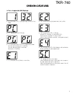
Page 5: ...2 displayed when the channel data is not written E3 displayed when PLL is unlocked Receiver PLL unlocked flashing BUSY LED Tansmitter PLL unlocked flashing TX LED Internal 19 2MHz reference unlocked flashing decimal point E4 displayed when PTT is attempted on a channel number that has no frequency data programmed SC displayed while in scan mode when the displayed channel is contained in scan seque...

Page 6: ... s PTT is disabled Local TX Disable Enable The local mic s PTT is toggled between disabled and enabled Scan Off Inhibits scanning Scan On Starts scanning Scan On Off Scanning is toggled between being enabled or inhibited Intercom On The Intercom feature is enabled Intercom Off The Intercom feature is disabled Intercom On Off The Intercom feature is toggled between enabled and disabled Voting Tone ...

Page 7: ...carrier and specified QT DQT are present TXS TX Sense This function becomes valid when the transmitter is keyed RX Unlock This alarm function becomes valid if the RX PLL circuitry becomes unlocked TX Unlock This alarm function becomes valid if the TX PLL circuitry become unlocked Exciter Temperature This alarm function becomes valid if the temperature of transmitter s exciter exceeds approximately...

Page 8: ...Turns on in Disable status Scan Off X O O Scan On X O O Scan On Off O O X Turns on in ON status Intercom On X O O Intercom Off X O O Intercom On Off O O X Turns on in ON status Voting Off X O O Voting On X O O Voting On Off O O X Turns on in ON status Take Over O X X Turns on in ON status QT DQT Encode Enable X O O QT DQT Encode Disable X O O QT DQT Encode Disable Enable O O X Turns on in Disable ...

Page 9: ...while transmitting TOT Enable X O O TOT Disable X O O TOT Disable Enable O O X Turns on in Disable status Hold Time Enable X O O Hold Time Disable X O O Hold Time Disable Enable O O X Turns on in Disable status Scrambler Off X O O Scrambler On X O O Scrambler On Off O O X Turns on in ON status Reset O O X Do not turn on None O O O Do not turn on Trigger Function PF Keys AUX Input Start Up Conditio...

Page 10: ...ed burst of the QT tone reverse burst when it detects the radio using the repeater has un keyed and also sent a reverse QT burst squelch tail elimination This mutes a receiving radio s speaker audio before its receiver circuit shuts off causes squelch tail noise in the speaker audio The TKR 740 can select the time between 140 to 200 ms that the QT reverse burst is sent Typically this time should n...

Page 11: ... Send CW ID to Remote RA function is set to Yes consequently the console can monitor the CW ID tone The TKR 740 contains 8 message banks for CW Message CW Message 1 to 8 is transmitted on the current channel when the CW Message 1 to 8 On function is activated respectively 11 PTT Priority A number of keying sources can be used to cause the TKR 740 to transmit The transmit audio path is switched acc...

Page 12: ...MT I O connector and 3 programmable AUX Input Ports 1 3 pins 4 6 and 6 programmable AUX Output ports pins 20 25 on the rear 25 pin D Sub connector The 7 programmable AUX I O pins are primarily intended for remote control interfaces Each AUX I O Port can be set for AUX Input AUX Output or remote Channel Select types The AUX Input port can be set execute a single input function or a set of up to thr...

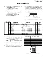
Page 13: ...us settings by means of the FPU through the RS 232C port Use to read and write frequency data and other features to and from the Repeater Use to check the Repeater using the PC This feature is included in the FPU Use to tune the Repeater using the PC This feature is included in the FPU Use when changing the Firmware program of the flash memory Mode User Mode PC Mode Firmware Programming Mode Opera...

Page 14: ... 4 2 Connection procedure Connect the TKR 740 to the personal computer IBM PC or compatible with the interface cable KPG 46 Connection is the same as in the PC Mode Note You can only program firmware from the 8 pin microphone connector on the front panel Using the 25 pin logic interface on the rear panel will not work 4 3 Programming 1 Start up the programming software KPG 47D select firmware prog...

Page 15: ...peaker Input Internal Speaker Input 2 I 10 TXCV TX VCO lock voltage check See Reference Table O 1 0 to 4 5V 11 RXCV RX VCO lock voltage check See Reference Table O 1 0 to 4 5V 12 SPO External Speaker Output 4W 4Ω 2 O 13 VC Voltage check of Power Source Impedance 10kΩ O 13 2V 14 FWD Voltage check of Forward power See Reference Table O 0 to 5V 15 EXT REF External reference check INT 5V EXT 0V O 0 or...

Page 16: ...mable Function output 1 4 O 0 or 5V 21 AUXO 2 Programmable Function output 2 4 O 0 or 5V 22 AUXO 3 Programmable Function output 3 4 O 0 or 5V 23 AUXO 4 Programmable Function output 4 4 O 0 or 5V 24 AUXO 5 Programmable Function output 5 4 O 0 or 5V 25 AUXO 6 Programmable Function output 6 4 O 0 or 5V Connector No Terminal Name Description I O Level CONTROL I O CONTROL I O 25pin D SUB jack Viewed fr...

Page 17: ...unction 2 4 I O 0 or 5V 12 AUX I O 7 Programmable Function 2 4 I O 0 or 5V Notes 1 Remote RA Receiver Audio output with de emphasis to Remote Terminal 400mVrms 4 7 kΩ Load Remote TA Transmit audio signal input from Remote terminal Impedance 600Ω Remote PTT Press to Talk for Remote Terminal transmit key 2 AUX I O 1 5 can be programmed for AUX Input AUX Output or BCD Channel Select AUX I O 6 7 can b...

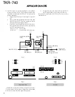
Page 18: ...rol external equipment 1 Program AUX I O 6 7 for AUX Output in the KGP 47D 2 Remove D32 R84 and R88 for AUX I O 6 D36 R83 and R87 for AUX I O 7 on the component side of control unit PCB see diagram below 3 Install Q14 Q15 and R154 for AUX I O 6 Q12 Q13 and R153 for AUX I O 7 on foil side of control unit PCB see diagram below Q12 13 14 15 DTD114EKA R153 154 3 9kΩ RK73GB1J392J chip resistor 4 Change...

Page 19: ...O 1 21 AUXO 2 22 AUXO 3 23 AUXO 4 24 AUXO 5 25 AUXO 6 1 Remote RA RX Audio output 2 Remote TA TX Audio input 3 Remote PTT PTT 4 EXT MON MON 5 GND TX return 6 AUX I O 1 F1 to F8 optionally 7 AUX I O 2 F1 to F8 optionally 8 AUX I O 3 F1 to F8 optionally 9 AUX I O 4 F1 to F8 optionally 10 AUX I O 5 F1 to F8 optionally 11 AUX I O 6 F1 to F8 optionally 12 AUX I O 7 F1 to F8 optionally 1 B AUX B Power 2...

Page 20: ...th TKR 740 and TKR 830 The cable for TKR 830 can be use for TKR 740 5 Adjust a LTR controller RX data RPT audio TX data etc according its installation manual 1 B 2 B 3 NC 4 GND 5 GND 6 SPG 7 RD 8 RSSI 9 SPI 10 TXCV 11 RXCV 12 SPO 13 VC 14 FWD 15 EXT REF 1 NC 2 RXD2 3 TXD2 4 AUXI 1 5 AUXI 2 6 AUXI 3 7 DG 8 TD 9 TA 10 RD 11 RA 12 RXG 13 SPM 14 NC 15 EXT_MON 16 EXT_PTT 17 SC 18 NC 19 TXG 20 AUXO 1 21...

Page 21: ... PF key or AUX Input If a PF key is programmed the Local Mic user must activate this during Intercom operation If an AUX Input is programmed a function or auxiliary function switch on the remote console must be used to activate the AUX Input prog for Remote TX Disable during Intercom operation Edit Optional features AUX I O Ports AUX Input Functions 12 pin 25 pin TX Disable Enable 2 3 Setting for ...

Page 22: ...board I RPTTI Remote PTT output to optional board O Remote PTT ON 0V OFF 5V RPTTO Remote PTT input from optional board I OPTION Enable Disable scrambler board O Scrambler ON 5V Scrambler OFF normally 0V CODE1 Scrambler code setting O 0V or 5V CODE2 Scrambler code setting O 0V or 5V CODE3 Scrambler code setting O 0V or 5V CODE4 Scrambler code setting O 0V or 5V 3 2 Connection to Optional Boards Ter...

Page 23: ...rated Relay or Tone Operated Relay COR or TOR output may be used alternative use the Squelch Control SC line on the 25 Pin D sub 10 Some ANI boards have a speaker mute output line Use the SPM line on the 25 Pin D sub 4 FPU Setting For Optional Board Voice scrambler 1 Select each item to enable for scrambler unit model TKR 740 158 174 Voice Scrambler OK 2 Select the channel s which will use scrambl...

Page 24: ... 2 Attach the fan enclosure to the front of the TKR 740 E heatsink so that the enclosure tabs are securely mounted to the heatsink chassis Chassis Front side 3 Guide the fan cable along with the front of the chassis and through the cable slot 4 Hook the fan cable around the cable holder then plug the connector into the CN104 on the TX unit A 3 CN104 TX UNIT A 3 CN104 Fan cable Cable holder ...

Page 25: ... to the chassis then plug the connector into the CN305 on the TX unit B 3 CN305 TX UNIT B 3 Slide the fan cable underneath the corner of the PCB How to install a coaxial cable between CN301 and CN1 TX unit When you connect CN1 TX unit A 3 and CN301 TX unit B 3 with a coaxial cable you must guide and align the coaxial cable with the shielded case as shown in the figure below Ensure that the coaxial...

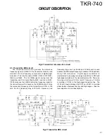
Page 26: ...z TX frequency range It has the following features High performance model with enhanced features 32 channel radio with 16 QT DQT Remote functions for use by base stations Fine frequency steps using Direct Digital Synthesizer DDS Signalling decoding and AF processing using Digital Signal Processor DSP Fig 1 Internal external reference circuit 2 Transmitter Unit The transmitter unit X56 307 A 3 cons...

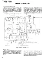
Page 27: ...he transmitter main PLL is 100 kHz the PLL frequency step is 100 kHz However fine CIRCUITDESCRIPTION Fig 2 Transmitter reference PLL circuit frequency steps such as 2 5kHz and 1 25kHz can be used because the DDS output frequency is variable IC202 performs binary FSK modulation Digital pager modulation is implemented by applying low range modulation to DDS and high range modulation to the transmitt...

Page 28: ...itter main PLL circuit produces the transmitter frequency signal and consists of VCO Q1 and Q2 and a single chip PLL IC IC101 Transmit frequencies from 146 000 MHz to 154 995 M Hz are derived from VCO Q1 Transmit frequencies from 155 000 MHz to 174 000 MHz are derived from VCO Q2 IC101 divides the VCO oscillator signal and the transmitter PLL reference signal 4 5 MHz and its phase is compared with...

Page 29: ...ence voltage setting for transmitter power adjustment are performed according to data from the CPU using the FPU IC105 is a modulation signal summing amplifier A 2 and a signalling signal amplitude fine adjustment amplifier B 2 IC102 is a splatter filter for digital pager modulation and has a two stage Butterworth filter with a cutoff frequency of 1 9kHz IC203 is a DC amplifier that amplifies the ...

Page 30: ...t The RFfinal amplifier unit X56 307 B 3 amplifies transmitter power to a specified level This unit consists of the following circuits 1 Transmitter power module 2 harmonic filter circuit 3 forward reflected power detector circuit 4 APC circuit 5 high temperature detector circuit 6 common mode spurious filter circuit 3 1 Transmitter power module The pow er module IC301 uses a pow er module RA30H13...

Page 31: ...ists of thermal switch TS301 and switching transistor Q302 This circuit disables the transmitter power amplifier to protect the circuits when the final unit temperature is too high 95 C or higher and the circuit cannot be operated safely Fig 11 APC circuit Fig 12 High temperature detector circuit Fig 13 Common mode spurious filter circuit 3 6 Common mode spurious filter circuit The TKR 740 has a f...

Page 32: ... only the desired signal to mixer DBM A1 Mixer DBM A1 mixes 4 Receiver Unit The receiver unit X55 305 consists of the following circuits 1 front end circuit 2 narrow IF circuit 3 wide IF circuit 4 receiver main PLL circuit 5 receiver DDS circuit 6 baseband circuit and 7 other circuits the first local oscillator signal generated by the first local crystal oscillator with the receive signal coming f...

Page 33: ...er IC15 B 2 AF amplifier IC11 A 2 and B 2 and goes to the Y0 input of multiplexer IC9 and the V2 input of electronic volume control IC9 The level of the signal that enters V2 of the electronic volume control IC is adjusted the signal passes through the hysteresis circuit AF switch Q34 goes to IC7 noise filter input pin 17 and high frequency components are selected by an HPF consisting of an extern...

Page 34: ...log switch IC21 invert amplifier IC15 A 2 and AF amplifier IC12 A 2 and goes to the Y1 input of multiplexer IC and the V1 input of electronic volume control IC9 The level of the signal that enters V1 of the electronic volume control IC is adjusted the signal passes through AF switch Q35 goes to IC8 noise filter input pin 17 and high frequency components are selected by an HPF consisting of an exte...

Page 35: ... The first local oscillator is an upper heterodyne local oscillator and the VCO oscillator frequency is 202 850 to 218 850 MHz In addition the two VCOs cover Fig 17 Receiver main PLL circuit two bands the Q8 VCO covers the lower band and the Q9 VCO covers the upper band PLL IC1 compares the 4 5MHz signal from the receiver DDS circuit and the VCO signal with the 100kHz comparison frequency ...

Page 36: ... wide FM detector circuits are de emphasized by LPF Q28 The sub audible components of the signal are removed by HPF Q26 and the resulting signal is switched with a squelch signal by D11 and Q29 and output as an RA signal from CN6 4 7 Other circuits In addition the receiver circuit contains an EEPROM IC10 as in the transmitter circuit Adjustment data for each unit and the last channel data are writ...

Page 37: ... 232C circuit and 9 power supply circuit CIRCUITDESCRIPTION 5 1 Main CPU The main CPU IC17 is a 16 bit single chip microcomputer containing a 128k ROM and a 5k RAM This CPU controls the sub CPU the flash ROM and the DSP encodes high speed and low speed data controls the transmitter unit the receiver unit the control unit and the display circuit and sends data to or from an external device Fig 21 M...

Page 38: ...s programmed so that it operates as the sub CPU by connecting its pin 18 to GND pin 18 of the main CPU is connected to Vdd The sub CPU functions as an I O expander and controls the flash ROM DSP and extended I O IC15 and IC16 are data bus buffer ICs Fig 22 Sub CPU CIRCUITDESCRIPTION ...

Page 39: ...2 low pass filter and goes to multiplexer IC37 The transmitter audio signal coming from pin 13 of IC29 is CIRCUITDESCRIPTION amplified by IC22 B 2 fed to pin 6 Vin R of codec IC27 and converted from analog to digital at a sampling frequency of 16 128 kHz The digitized transmitter audio signal is AGC processed pre emphasized and filtered at 300 Hz to 3 kHz by DSP IC30 and the resulting signal is fe...

Page 40: ...rnal red external reference state LEDs in switches S700 to S705 IC700 IC701 IC702 and IC703 to display this model channels Fig 25 Display circuit Fig 24 AF PA circuit CIRCUITDESCRIPTION pin test connector SPO SPG on the rear panel The impedance of the internal speaker is adjusted to provide an audio output of about 0 2 W when the internal speaker installed on this model front panel is used and sta...

Page 41: ...7 and IC40 Modulation inputs include local microphone input low speed data LSD high speed data HSD external audio input TA external data input TD and remote Fig 26 Baseband circuit modulation input RTA and demodulation outputs include receive audio output RA receive dataoutput RD and remote receive audio RRA The multiplexer IC14 IC29 IC37 changes signals the electronic volume control IC33 adjusts ...

Page 42: ...ata required for this function is also transferred through the RS 232C serial port The firmware can only be rewritten using the local microphone connector on the front panel Fig 28 RS 232C circuit Fig 29 Power supply circuit 5 9 Power supply circuit The power supply circuit generates power to operate the CPU DSP flash ROM bi directional buffer and baseband circuit This circuit consists of IC3 IC4 ...

Page 43: ...A19 O Not used 50 59 A18 9 O Flash memory address bus 60 Vcc 5V 61 A8 O Flash memory address bus 62 Vss GND 63 70 A7 0 O Flash memory Sub CPU address bus 71 IWR O DSP IDMA write output 72 IRD O DSP IDMA read output 73 IAL O DSP IDMA address latch output 74 IS O DSP IDMA select output 75 PF3 O DSP RX mute control output 76 PF2 Not used 77 PF1 O DSP modulation control output 78 PF0 Not used 79 86 D7...

Page 44: ... Acknowlege Main CPU 59 Vdd Vdd 60 GND GND 61 IS I IDMA Select pull up Main CPU 62 IAL I IDMA Address Latch pull up Main CPU 63 IRD I IDMA Read Enable pull up Main CPU 64 IWR I IDMA Write Enable pull up Main CPU 65 D8 I O Data I O NC 66 GND GND 67 Vdd Vdd 68 70 D9 11 I O Data I O NC 71 GND GND 72 79 D12 19 I O Data I O NC 80 GND GND 81 84 D20 23 I O Data I O NC 85 FL2 O Output Frag CODEC MC termin...

Page 45: ... Pin 25 50 70mW Po 30W Parasitic LOAD VSWR 3 1 oscillation SEMICONDUCTORDATA POWERMODULE RA30H1317M TX UNIT IC301 MAXIMUM RATINGS Tc 25 C Zg ZI 50Ω Vdd SUPPLY VOLTAGE Vgg 5 0V Zg ZI 50Ω 17 V Vgg GATE BIAS VOLTAGE Vdd 12 5V Pin 50mW 6 V Zg ZI 50Ω Idd DRAIN CURRENT 10 A Pin INPUT POWER f 135 175MHz Vgg 5 0V 100 mW Po OUTPUT POWER f 135 175MHz Vgg 5 0V 45 W Tc op OPERATION CASE TEMPERATURE f 135 175M...

Page 46: ... SW D11 DIODE SQ SW REF No Parts name DESCRIPTION CONTROL UNIT X53 3882 71 IC1 IC MULTIPLEXER IC3 6 IC AVR IC7 IC FLASH ROM IC10 IC VOLTAGE DETECTOR IC12 13 IC AF AMP IC14 IC MULTIPLEXER IC15 16 IC BUS BUFFER IC17 18 IC CPU IC22 23 IC AF AMP IC24 IC COUNTER IC25 IC INVERTER IC27 IC CODEC IC29 IC MULTIPLEXER IC30 IC DSP IC31 32 IC AF AMP IC33 IC D A CONVERTER IC34 IC AF AMP IC35 IC MULTIPLEXER IC36...

Page 47: ...112 FET SQ SWITCH Q113 FET DC SWITCH Q114 TRANSISTOR DC SWITCH Q115 TRANSISTOR RF AMP Q201 TRANSISTOR VCO OSC Q202 TRANSISTOR BUFFER AMP Q203 FET DC SWITCH Q205 TRANSISTOR RF AMP Q206 FET DC SWITCH Q207 TRANSISTOR INVERTER Q208 FET DC SWITCH Q240 TRANSISTOR BUFFER AMP Q241 TRANSISTOR RF AMP Q242 TRANSISTOR BUFFER AMP PIN No Parts name DESCRIPTION Q301 TRANSISTOR DC AMP Q302 304 TRANSISTOR DC SWITC...

Page 48: ...K73G B1H472K C HIPC 4700P F K C 86 C K73G B1H472K C HIPC 4700P F K C 87 C K73G B1H152K C HIPC 1500P F K C 88 C K73E B1C 105K C HIPC 1 0UF K C 89 C C 73F C H1H751J C HIPC 750P F J CONTROL UNIT X53 3882 71 1 3A A62 0726 03 P ANE L F R O NT 2 3A 1E B10 2590 04 F R O NTG LASS 3 3B B11 1223 04 F ILTE R P FKE YS 4 3A B11 1225 04 F ILTE R F R O NTP ANE L LE D 5 3B B11 1231 04 F ILTE R F R O NTP ANE L 7SE...

Page 49: ...HIPC 22P F J C 191 C K73F B1C 105K C HIPC 1 0UF K C 192 C K73G B1E 103K C HIPC 0 010UF K C 193 C K73F B1E 104K C HIPC 0 10UF K C 194 C 92 0628 05 C HIP TAN 10UF 10WV C 200 202 C K73G B1H471K C HIPC 470P F K C 203 C K73G B1E 103K C HIPC 0 010UF K C 204 C K73G B1H471K C HIPC 470P F K C 205 C K73G B1E 103K C HIPC 0 010UF K C 206 C 92 0628 05 C HIP TAN 10UF 10WV C 207 C 92 0771 05 C HIP E LE 220UF 6 3...

Page 50: ... 16W R 104 R K73G B1J333J C HIPR 33K J 1 16W R 105 R K73G B1J223J C HIPR 22K J 1 16W R 106 R K73G B1J224J C HIPR 220K J 1 16W R 107 108 R K73G B1J223J C HIPR 22K J 1 16W R 109 R K73G B1J473J C HIPR 47K J 1 16W R 110 R K73G B1J334J C HIPR 330K J 1 16W R 114 120 R 92 0670 05 C HIPR 0O HM R 121 R K73G B1J333J C HIPR 33K J 1 16W R 122 R K73G B1J104J C HIPR 100K J 1 16W R 123 R K73G B1J103J C HIPR 10K ...

Page 51: ...289 R K73G B1J473J C HIPR 47K J 1 16W R 290 R K73G B1J101J C HIPR 100 J 1 16W R 291 R K73G B1J472J C HIPR 4 7K J 1 16W R 292 R K73G B1J473J C HIPR 47K J 1 16W R 293 R K73G B1J101J C HIPR 100 J 1 16W R 294 296 R K73G B1J473J C HIPR 47K J 1 16W R 297 301 R K73G B1J101J C HIPR 100 J 1 16W R 302 305 R K73G B1J102J C HIPR 1 0K J 1 16W R 306 R K73G B1J103J C HIPR 10K J 1 16W R 307 R K73G B1J473J C HIPR ...

Page 52: ... C HIPC 12P F G C 22 C K73G B1H102K C HIPC 1000P F K C 23 C C 73G C H1H040C C HIPC 4 0P F C C 24 C K73G B1H103K C HIPC 0 010UF K C 25 C C 73F C H1H470J C HIPC 47P F J C 26 C K73G B1H102K C HIPC 1000P F K C 27 C K73G B1H103K C HIPC 0 010UF K C 28 C K73F B1E 104K C HIPC 0 10UF K C 29 C K73G B1H103K C HIPC 0 010UF K C 30 31 C K73G B1H102K C HIPC 1000P F K C 32 C C 73F C H1H150G C HIPC 15P F G C 33 C ...

Page 53: ...000P F K C 165 C 92 0003 05 C HIP TAN 0 47UF 25WV C 166 C C 73G C H1H080D C HIPC 8 0P F D C 167 C K73F B1E 104K C HIPC 0 10UF K C 168 C K73G B1H103K C HIPC 0 010UF K C 169 170 C 92 0628 05 C HIP TAN 10UF 10WV C 171 C 92 0003 05 C HIP TAN 0 47UF 25WV C 172 173 C K73F B1E 104K C HIPC 0 10UF K C 174 175 C K73G B1H102K C HIPC 1000P F K C 176 177 C K73F B1E 104K C HIPC 0 10UF K C 178 179 C K73G B1H221K...

Page 54: ...R 20 R K73F B2A100J C HIPR 10 J 1 10W R 21 R K73G B1J561J C HIPR 560 J 1 16W R 22 R K73G B1J102J C HIPR 1 0K J 1 16W R 23 R K73G B1J122J C HIPR 1 2K J 1 16W R 24 R 92 1252 05 C HIPR 0O HM J 1 16W R 25 R K73F B2A100J C HIPR 10 J 1 10W R 26 R K73G B1J101J C HIPR 100 J 1 16W R 28 R 92 1252 05 C HIPR 0O HM J 1 16W R 29 R K73G B1J473J C HIPR 47K J 1 16W R 30 R K73G B1J101J C HIPR 100 J 1 16W R 32 R K73...

Page 55: ... 158 R K73G B1J472J C HIPR 4 7K J 1 16W R 159 R K73G B1J272J C HIPR 2 7K J 1 16W R 160 R K73G B1J472J C HIPR 4 7K J 1 16W R 161 R K73G B1J272J C HIPR 2 7K J 1 16W R 162 R K73G B1J152J C HIPR 1 5K J 1 16W R 163 R K73G B1J102J C HIPR 1 0K J 1 16W R 164 165 R K73G B1J473J C HIPR 47K J 1 16W R 166 R K73G B1J474J C HIPR 470K J 1 16W R 167 R K73G B1J224J C HIPR 220K J 1 16W R 168 R K73G B1J122J C HIPR 1...

Page 56: ...C K73G B1H471K C HIPC 470P F K C 56 C C 73G C H1H471J C HIPC 470P F J C 57 C 92 0560 05 C HIP TAN 10UF 6 3WV C 58 59 C K73G B1H102K C HIPC 1000P F K C 60 C K73G B1H471K C HIPC 470P F K C 61 C K73G B1H102K C HIPC 1000P F K C 62 63 C K73G B1H471K C HIPC 470P F K C 64 65 C C 73G C H1H101J C HIPC 100P F J C 66 C K73G B1H102K C HIPC 1000P F K C 68 C K73G B1H103K C HIPC 0 010UF K C 69 C K73G B1H102K C H...

Page 57: ... 470P F K C 272 C C 73G C H1H470J C HIPC 47P F J C 273 274 C K73F B1E 104K C HIPC 0 10UF K C 275 C K73G B1H102K C HIPC 1000P F K C 276 C K73F B1E 104K C HIPC 0 10UF K C 277 C C 73G C H1H560J C HIPC 56P F J C 278 281 C K73G B1H102K C HIPC 1000P F K C 282 C K73G B1H103K C HIPC 0 010UF K C 283 C C 73G C H1H271J C HIPC 270P F J C 284 C K73G B1H103K C HIPC 0 010UF K C 285 C C 73G C H1H330J C HIPC 33P F...

Page 58: ... C HIPR 10K J 1 16W R 15 R K73G B1J471J C HIPR 470 J 1 16W R 16 R K73G B1J103J C HIPR 10K J 1 16W R 17 R K73G B1J473J C HIPR 47K J 1 16W R 18 R K73G B1J103J C HIPR 10K J 1 16W R 19 R K73G B1J470J C HIPR 47 J 1 16W R 20 R K73G B1J103J C HIPR 10K J 1 16W R 21 R K73G B1J471J C HIPR 470 J 1 16W R 22 R K73G B1J103J C HIPR 10K J 1 16W R 23 R K73G B1J183J C HIPR 18K J 1 16W R 24 R K73G B1J101J C HIPR 100...

Page 59: ...J C HIPR 100K J 1 16W R 217 218 R K73G B1J471J C HIPR 470 J 1 16W R 219 R K73G B1J103J C HIPR 10K J 1 16W R 220 R K73G B1J473J C HIPR 47K J 1 16W R 221 R K73G B1J560J C HIPR 56 J 1 16W R 222 R K73G B1J103J C HIPR 10K J 1 16W R 223 R K73G B1J153J C HIPR 15K J 1 16W R 224 R K73G B1J223J C HIPR 22K J 1 16W R 225 R K73G B1J103J C HIPR 10K J 1 16W R 226 R K73G B1J124J C HIPR 120K J 1 16W R 227 R K73G B...

Page 60: ...IC IC 105 NJM4558E MO SIC IC 106 AT24C 08N10SI18 R O M IC IC 107 NJM4558E MO SIC IC 108 NJM78L08UA BI P O LARIC IC 109 NJM2904E MO SIC IC 110 NJM78L05UA BI P O LARIC IC 200 TC 4S81F MO SIC IC 201 C D8468 MO SIC IC 202 AD9835BR U MO SIC IC 203 NJM2904E MO SIC IC 204 NJM2903M MO SIC IC 205 NJM78L05UA BI P O LARIC IC 206 TC 74HC 14AF MO SIC IC 301 R A30H1317M MO SIC IC 302 303 O P 291G S BI P O LARIC...

Page 61: ...Hx10 Ex11 Ax3 Ax14 Ax10 Ax10 Ax11 Ex2 Ax3 E 14 715 708 710 708 704 705 706 707 22 20 17 12 14 7 717 36 33 35 19 19 34 38 37 Gx2 50x2 716 X53 A 4 X56 C 3 28 IC301 25 44 F F 24 23 24 EXPLODEDVIEW Parts with the exploded numbers larger than 700 are not supplied TKR 740 TKR 740 62 61 A M3x5 N32 3005 45 B M4x8 N32 4008 45 C M3x6 N35 3006 46 D M3x6 N67 3006 46 E M2 6x6 N87 2606 46 F M2 6x10 N87 2610 46 ...

Page 62: ...4 6 INSTRUCTION MANUAL B62 1700 00 21 SQUARE PLUG E59 0410 05 9 LEAD WIRE WITH CONNECTOR E31 3228 05 42 PROTECTION BAG H25 0720 04 8 DC CORD E30 3344 15 702 39 POLYSTYRENE FOAMED FIXTURE H10 6612 02 39 POLYSTYRENE FOAMED FIXTURE H10 6612 02 40 PROTECTION COVER H20 1437 03 43 ITEM CARTON CASE H52 1966 02 Parts with exploded numbers larger than 700 are not supplied ...

Page 63: ...T High temperature detect I 14 CP TX both PLL clock signal O 15 NC No connection 16 DP TX both PLL data signal O 17 EXR Exit reference detector I 18 CVT TX main PLL lock voltage I 19 REV Reverse TX power detector I 20 FWD Forward TX power detector I 21 GND Ground 22 PAG Digital pager signal O 23 B Power supply Vcc I 24 B Power supply Vcc I 25 B Power supply Vcc I 26 PAB Power supply for AF PA IC I...

Page 64: ...ction 26 NC No connection 27 NC No connection 28 NC No connection 29 NC No connection 30 NC No connection 1 B Power supply Vcc O 2 FWD TX forward power detect signal O 3 EXR External reference detect signal O 4 CVT TX main PLL lock voltage signal O 5 CVR RX main PLL lock voltage signal O 6 RD RX data data voice O 7 RSSI RX signal strength indicator signal O 8 SPO External Speaker AF O 9 SPO Extern...

Page 65: ...rophone signal O 26 MIG Microphone ground 1 SPG Internal Speaker ground 2 SP Internal Speaker AF output O 1 VLO AF signal for VR701 I 2 VLI AF signal from VR701 O 3 GND Ground 4 BLT Mic connector J700 pin1 5 B Power supply Vcc I 6 GND Ground 7 PTT Press to talk switch O 8 MIG Microphone ground 9 MIC Microphone signal O 10 HOK Hook signal O 11 MDAT Mic connector J700 pin8 12 NC No connection 13 NC ...

Page 66: ...VT TX main PLL lock voltage O 19 REV Reverse TX power detector O 20 FWD Forward TX power detector O 21 GND Ground 22 PAG Digital pager signal I 23 B Power supply Vcc O 24 B Power supply Vcc O 25 B Power supply Vcc O 26 PAB Power supply for AF PA IC O EXT REF External reference signal input coaxial I REF OUT RX reference signal output coaxial O Terminal No Terminal name Terminal function I O CN102 ...

Page 67: ...LL strobe signal I 16 LDR RX PLL lock detector O 17 GND Ground 18 CVR RX main PLL lock voltage O 19 NC No connection 20 NC No connection 21 B Power supply Vcc I 22 B Power supply Vcc I 23 B Power supply Vcc I 24 NC No connection 25 NC No connection 26 NC No connection CN6 Terminal No Terminal name Terminal function I O CN7 Terminal No Terminal name Terminal function I O REF IN Reference signal inp...

Page 68: ...ivity Frequency Range 10Hz to 600MHz Frequency Counter Frequency Stability 0 2ppm or less 7 Ammeter 10A or more 8 AF Volt Meter Frequency Range 50Hz to 10kHz AF VTVM Voltage Range 3mV to 3V 9 Audio Generator AG Frequency Range 50Hz to 5kHz Output 0 to 1V 10 Distortion Meter Capability 3 or less at 1kHz Input Level 50mV to 10Vrms 11 Voltmeter Measuring Range 10 to 1 5V DC or less Input Impedance 50...

Page 69: ...OUT FUSE L44 L43 L40 CONTROL I O EXT REF IN 1 13 25 14 RA RD TA TD TEST SPKR REMT I O SP 1 2 3 4 5 6 7 8 9 10 11 12 13 14 15 1 2 3 4 5 6 7 8 9 10 11 12 ADJUSTMENT Adjustment Location Top view Section Arrangement Top view FINAL UNIT or EXCITER UNIT TX UNIT RX UNIT CONTROL UNIT X56 3072 70 B 3 X53 3882 71 X55 3050 11 X56 3072 70 A 3 C 3 ...

Page 70: ...H B Low A Hi For production Center TX RX 17 164 4000 152 4000 No Wide H A High Helical Center Low edge 18 167 6000 155 6000 No Wide H B Low Helical Center High edge 19 164 4000 152 4000 No Narrow L A High Helical Center Low edge 20 167 6000 155 6000 No Narrow L B Low Helical Center High edge 21 159 6000 159 6000 No Wide H A Low Helical Low High edge 22 159 6000 159 6000 No Narrow L A Low Helical L...

Page 71: ...then connect CN5 CN3 L32 Adjust it to look like Refer to page 80 to the spectrum analyzer input CN5 L28 the wave on page 80 1 CH10 L39 L41 L44 5 Discriminator Connect the SSG to RX IN SSG TEST SPKR L52 Adjust for maximum Adjust 1 CH4 AFVM SPO Terminal Wide MOD 1kHz pin 12 DEV 2 4kHz SSG 501µV 53dBm AF 0 45V 4Ω Narrow 1 CH10 L53 MOD 1kHz DEV 1 5kHz SSG 501µV 53dBm AF 0 45V 4Ω 6 Sensitivity 1 Connec...

Page 72: ...OD 1kHz Wide DEV 2 4kHz SSG 3dB below to 12dB SINAD level AF 0 45V 4Ω Narrow 1 Connect the SSG to RX IN then select the channel that the user will use Narrow MOD 1kHz DEV 1 5kHz SSG 3dB below to 12dB SINAD level AF 0 45V 4Ω 9 RX S N 1 Connect the SSG to RX IN then select the Check 56dB or less Check channel that the user will use Wide Wide MOD 1kHz DEV 2 4kHz SSG 501µV 53dBm AF 2 84V 4Ω Narrow 1 C...

Page 73: ...g 1 CH4 Center Frequency AFVM CONTROL I O PC ADJ Pilot Tone Voting Pilot Tone 1950Hz RA Terminal 400mV 20mV Adjust SSG OFF pin 11 Wide Narrow 1 CH10 Center Frequency Voting Pilot Tone 1950Hz SSG OFF RX UNIT Item Condition Measurement Adjustment Specifications Test Unit Terminal Unit Parts Method Remarks equipment TX UNIT 14 TX Lock 1 CH3 TX A Hi DVM TX CV TX TC1 4 5V ADJ 0 1V Voltage 2 CH1 TX A Lo...

Page 74: ...IC 3 4kHz 3 CH3 VCO A Hi Terminal 4 CH4 VCO B Lo pin 6 5 CH5 VCO B Center 6 CH6 VCO B Hi MOD 1kHz LEVEL 50mV Terminal load LPF 15kHz HPF OFF Transmission Narrow 1 CH7 VCO A Lo PC ADJ 0 1kHz 2 CH8 VCO A Center 1 7kHz 3 CH9 VCO A Hi 4 CH10 VCO B Lo 5 CH11 VCO B Center 6 CH12 VCO B Hi MOD 1kHz LEVEL 50mV Terminal load LPF 15kHz HPF OFF Transmission 20 Mic 1 CH2 VCO A Center MOD ANA TX TX OUT Check 2 ...

Page 75: ... 75kHz 0 05kHz Wide AG f 100Hz Sine wave LEVEL Insert 0 5Vp p into the CONTROL I O TD terminal pin 8 LPF 3kHz HPF OFF Transmission Narrow 1 CH8 VCO A Center 2 CH11 VCO B Center AG f 100Hz Sine wave LEVEL Insert 0 5Vp p into the CONTROL I O TD terminal pin 8 LPF 3kHz HPF OFF Transmission 23 TA Dev 1 CH4 Center Frequency TX OUT PC ADJ Adjust AG f 1kHz Sine wave CONTROL I O 2 4kHz 0 1kHz Wide LEVEL I...

Page 76: ...smission Narrow 1 CH10 Center Frequency PC ADJ AG f 1kHz Sine wave 1 5kHz 0 05kHz LEVEL Insert 280mV into the REMT I O Remote TA terminal pin 2 LPF 15kHz HPF OFF Transmission 26 RTA Dev 1 CH2 VCO A Center Check 2 4kHz 0 1kHz Check 2 CH5 VCO B Center Wide AG f 1kHz Sine wave LEVEL 280mV LPF 15kHz HPF OFF Transmission Narrow 1 CH8 VCO A Center Check 1 5kHz 0 05kHz 2 CH11 VCO B Center AG f 50kHz LEVE...

Page 77: ...0 DQT Dev 1 CH2 VCO A Center Check 0 60kHz 0 1kHz Check 2 CH5 VCO B Center Wide DQT 023N LPF 3kHz HPF OFF Detector Peak Hold Transmission Narrow 1 CH8 VCO A Center 0 35kHz 0 05kHz 2 CH11 VCO B Center DQT 023N Transmission 31 Test Tone 1 CH4 Center Frequency PC ADJ Dev TEST TONE 1kHz 2 4kHz 0 1kHz Adjust LPF 15kHz Wide HPF OFF Transmission Narrow 1 CH10 Center Frequency PC ADJ TEST TONE 1kHz 1 5kHz...

Page 78: ...J 102 Shift Level writing Writing 35 Pager 1 CH2 VCO A Center Make the demodulated Waveform 2 CH5 VCO B Center wave square Balance LPF 3kHz Adjust HPF OFF Oscilloscope Transmission DC range 36 TX S N 1 CH2 VCO A Center CONTROL I O Check 54dB or less Check 2 CH5 VCO B Center TA Terminal Wide No modulation pin 9 LPF 3kHz HPF 300Hz De emphasis 750µS Transmission Narrow 3 CH8 VCO A Center 53dB or less...

Page 79: ...TKR 740 80 ADJUSTMENT BPF wave MCF wave Wide Narrow Example The wave will look like this when using a frquency of 166 000 MHz Factory default setting 166 000MHz ...

Page 80: ...R350 R351 R352 R45 R46 R47 R48 R66 R70 R71 R76 R78 R80 X1 X2 IC17 R149 R150 R151 R152 C77 C87 C89 C167 IC4 IC6 L1 L7 L11 C168 R69 L13 C1 C10 C102 C108 C11 C12 C13 C207 C210 C211 C300 C15 C301 C302 C303 C304 C305 C306 C307 C308 C309 C310 C311 C312 C317 C318 C327 C328 C329 C330 C331 C332 C333 C335 C336 C337 C4 C5 C7 C9 R1 R100 R101 R103 R104 R219 R220 R302 R303 R304 R305 R306 R319 R320 R321 R322 R32...

Page 81: ...315 C316 C319 C320 C321 C322 C61 C80 CP10 CP11 CP14 CP15 IC15 IC16 IC35 IC46 IC47 IC48 R126 R127 R129 R130 R138 R139 R145 R146 R147 R148 C181 C212 C213 C214 R16 C136 D18 C127 C14 D21 IC1 R189 R2 IC49 Q12 R125 C130 R180 Q2 R9 J72 0668 11 X53 3882 71 A 4 A B C D E F G H I J K L M N O P Q R S 1 3 4 5 6 7 8 9 10 11 12 13 14 2 Component side Foil side Layer 1 Layer 2 Layer 3 Layer 4 TKR 740 PCBOARD 83 ...

Page 82: ...R205 R206 R207 R208 R209 R210 R211 R212 R213 R217 R227 R228 R229 R230 R231 R232 R233 R234 R235 R236 R238 R241 R243 R244 R246 R249 R251 R252 R254 R256 R257 R263 R267 R274 R28 R281 R284 R286 R287 R288 R29 R290 R291 R293 R295 R297 R298 R299 R30 R300 R301 R31 R32 R343 R344 R345 R346 R347 R348 R349 R350 R351 R352 R45 R46 R47 R48 R66 R70 R71 R76 R78 R80 X1 X2 IC17 R149 R150 R151 R152 C77 C87 C89 C167 IC...

Page 83: ...C734 C735 D710 C725 C742 R707 R708 J72 0668 11 X53 3882 71 B 4 A B C D E F G H I J K L M N O P Q R S 1 3 4 5 6 7 8 9 10 11 12 13 14 2 TKR 740 PCBOARD 87 88 CONTROL UNIT X53 3882 71 B 4 Component Side View J72 0668 11 CONTROL UNIT X53 3882 71 B 4 Foil Side View J72 0668 11 CONTROL UNIT X53 3882 71 B 4 Component Side Foil Side View J72 0668 11 O N f e R s s e r d d A 3 2 C I C 5 3 0 7 C I D 8 6 0 7 ...

Page 84: ...5 R716 R719 R733 J700 J72 0668 11 X53 3882 71 C 4 C720 C722 C736 C737 R720 R722 R731 R732 J72 0668 11 X53 3882 71 C 4 A B C D E F G H I J K L M N O P Q R S 1 3 4 5 6 7 8 9 10 11 12 13 14 2 TKR 740 PCBOARD CONTROL UNIT X53 3882 71 C 4 Component Side View J72 0668 11 90 89 CONTROL UNIT X53 3882 71 D 4 Component Side View J72 0668 11 CONTROL UNIT X53 3882 71 C 4 Foil Side View J72 0668 11 CONTROL UNI...

Page 85: ... IN CF1 SUB PLL CV R210 R254 C70 L4 Q6 D6 D5 R5 R7 C28 R13 C14 R21 R54 R27 C20 R22 R24 C33 C30 R14 R23 C35 R18 R16 L11 R17 C26 R47 R6 R8 C12 C27 R15 R20 R19 C23 C25 C21 C119 R261 C231 C233 C234 L244 L245 C69 C143 C146 R134 R136 R84 R114 R124 R101 R105 C239 L16 R192 R191 R190 R240 R245 R247 C74 C75 C76 C214 R214 C286 C202 C204 C218 C221 C222 R60 C285 R222 R223 C167 R150 R183 R184 Q208 R149 C186 R18...

Page 86: ...58 R89 C54 R42 R45 R44 R43 C172 R151 R85 Q13 C171 C19 C15 R12 R11 C6 C68 R109 C16 R9 R10 C22 C24 R132 R133 R141 R144 C64 C120 C226 L17 C125 IC206 1 7 14 8 R206 D204 C232 C213 C216 R216 R217 L207 C277 Q202 R112 R106 R108 C106 C187 R86 C188 R87 R88 C207 R61 X56 3072 70 A 3 J72 0879 09 A B C D E F G H I J K L M N O P Q R S 1 3 4 5 6 7 8 9 10 11 12 13 14 2 TKR 740 PCBOARD TX UNIT X56 3072 70 A 3 Foil ...

Page 87: ...MOD Q5 Q2 Q1 C73 C115 C132 C273 C276 D50 D51 D52 IC200 1 3 5 4 L106 Q17 Q18 R58 R59 R64 R205 R207 C258 C210 C282 C284 L203 L209 Q201 R224 R225 IC201 1 10 20 11 X201 C165 C166 XF211 C212 IC101 1 10 20 11 R180 R181 R182 1 4 8 5 Q21 5 3 4 1 2 R57 L247 L248 L5 L6 L7 R272 IC202 1 8 16 9 L205 Q107 SUB PLL Q241 C246 C283 C288 R130 C292 C293 IC1 OUT GND IN CF1 SUB PLL CV R210 R254 C70 L4 Q6 D6 D5 R5 R7 C2...

Page 88: ...8 C334 R357 C341 R358 R359 R360 R303 R304 R305 C319 C320 C330 R322 R339 R328 L301 L302 L303 R327 C413 C412 C411 C410 C420 C306 D320 C431 C432 Q309 C425 X56 3072 70 B 3 J72 0879 09 X56 3072 70 C 3 J72 0879 09 A B C D E F G H I J K L M N O P Q R S 1 3 4 5 6 7 8 9 10 11 12 13 14 2 TKR 740 PCBOARD TX UNIT X56 3072 70 B 3 C 3 Component Side View J72 0879 09 98 97 O N f e R s s e r d d A 2 0 3 C I M 5 3...

Page 89: ...72 70 B 3 J72 0879 09 X56 3072 70 C 3 J72 0879 09 A B C D E F G H I J K L M N O P Q R S 1 3 4 5 6 7 8 9 10 11 12 13 14 2 TKR 740 PCBOARD 99 100 TX UNIT X56 3072 70 B 3 C 3 Foil Side View J72 0879 09 O N f e R s s e r d d A 0 0 5 D P 8 TX UNIT X56 3072 70 C 3 Component side Foil side Layer 1 Layer 2 Layer 3 Layer 4 ...

Page 90: ... R355 R300 R308 C334 R357 C341 R358 R359 R360 R303 R304 R305 C319 C320 C330 R322 R339 R328 L301 L302 L303 R327 C413 C412 C411 C410 C420 C306 D320 C431 C432 Q309 C425 X56 3072 70 B 3 J72 0879 09 X56 3072 70 C 3 J72 0879 09 A B C D E F G H I J K L M N O P Q R S 1 3 4 5 6 7 8 9 10 11 12 13 14 2 TKR 740 PCBOARD TX UNIT X56 3072 70 B 3 C 3 Component Side Foil Side View J72 0879 09 102 101 TX UNIT X56 3...

Page 91: ...2 R116 Q8 Q9 C217 C218 LO GND GND GND IF RF L1 IC6 1 8 16 9 LD 5C1 RA RXG DET DEG SC RSSI CK DT ESR EVR SCL SDA DP CP EPR LDR GND CVR NC NC B B B NC NC NC Q34 R28 CF5 C222 R20 R25 R71 R82 R97 CV1 R170 R172 R182 R192 C137 IC15 1 4 8 5 C59 R22 R23 C142 R193 C108 C106 C204 C155 C156 C163 L20 R140 C144 C149 C152 L30 R144 X2 C20 R69 C13 R195 R199 C29 C37 L33 L55 C226 C229 C48 C56 CP1 IC20 1 8 16 9 R35 ...

Page 92: ... C211 L45 R122 R124 R125 R127 C139 C162 C164 R130 R139 R145 C166 C168 R142 L47 C195 R159 R79 R13 R15 C111 C112 IC18 1 3 5 4 R75 C9 C104 C131 L24 R59 R60 R63 R66 C160 C213 R196 R197 R198 R52 C228 C62 C72 Q33 Q39 Q30 C55 R14 R70 C220 L58 C80 L26 C70 C19 C24 C31 C36 L13 R21 R179 R180 C18 C84 L64 L65 L66 C38 IC17 O G I X55 3050 11 J72 0666 01 A B C D E F G H I J K L M N O P Q R S 1 3 4 5 6 7 8 9 10 11...

Page 93: ...C71 C75 C79 R16 R42 R43 R62 R73 R74 C207 C208 C209 IC13 1 26 O G I CN3 1 2 CN4 1 2 CN5 L19 L21 L23 IC14 1 4 8 5 IC16 I G O R186 TH1 TH2 C26 C33 C88 L11 L14 L15 L17 L2 L4 L6 L7 L9 C105 C210 D11 Q6 Q10 Q12 Q13 Q14 X55 3050 11 J72 0666 01 Q17 Q18 Q19 Q22 8C3 8C2 Q26 Q28 Q29 IC4 IN GND OUT C135 C143 C5 L49 L50 L56 Q1 R11 R183 C171 Q3 R55 C101 C14 L16 L3 C82 R116 Q8 Q9 C217 C218 LO GND GND GND IF RF L1...

Page 94: ...A B C D E F G J H K L M N P O Q R S 1 2 3 4 5 6 7 TKR 740 SCHEMATICDIAGRAM Note The components marked with a dot are parts of layer1 ...

Page 95: ...T U V W X Y Z AB AA AC AD AE AF AH AG AI AJ AL AK 1 2 3 4 5 6 7 TKR 740 SCHEMATICDIAGRAM Note The components marked with a dot are parts of layer1 ...

Page 96: ...AM AN AO AP AQ AR AS AU AT AV AW AX AY BA AZ BB BC BE BD 1 2 3 4 5 6 7 TKR 740 SCHEMATICDIAGRAM Note The components marked with a dot are parts of layer1 ...

Page 97: ...TKR 740 TKR 740 BLOCKDIAGRAM 121 122 ...

Page 98: ...t level 60 modulation Even though the speech output terminal reaches 4W when receiving low frequencies you need a 1kHz AF signal level Even though the modulation reaches 60 when transmitting low frequencies you need a 1kHz MIC input level Measure the level of transmitted high frequencies directly from a special quality 50Ω impedance spec trum analyzer ...

Page 99: ...TKR 740 TKR 740 INTERCONNECTION DIAGRAM 125 126 ...

Page 100: ... is turned OFF 2 When using the external speaker remove the jumper lead from the connector and attach the speaker cable 3 When not using the external speaker replace the jumper lead and insert the connector into the speaker jack pins 9 and 12 7 SPECIFICATIONS Specifications KES 4 Speaker size 120mm Maximum input power 20W Impedance 4 ohms Frequency response 100 to 5000 Hz Dimensions W H D 127 127 ...

Page 101: ...MEMO 129 ...

Page 102: ...z Microphone Impedance 600Ω Band Spread 28MHz EXT Reference Sensitivity 10MHz 50Ω 10dBm SPECIFICATIONS TKR 740 KENWOOD follows a policy of continuous advancement in development For this reason specifications may be changed without notice KENWOOD CORPORATION 2967 3 Ishikawa machi Hachioji shi Tokyo 192 8525 Japan KENWOOD U S A CORPORATION P O BOX 22745 2201 East Dominguez Street Long Beach CA 90801...

Reviews: