TK-3170/3173
24
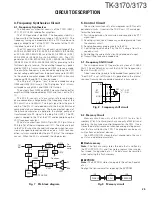
2-5. Audio Amplifier Circuit
The demodulated signal from IC701 is amplified by IC10,
and goes to AF amplifier through IC13.
The signal then goes through an volume control (IC16),
and is routed to an audio power amplifier (IC18) where it is
amplified and output to the speaker.
2-6. Squelch Circuit
Part of the AF signal from the IC enters the FM IC (IC701)
again, and the noise component is amplified and rectified by a
filter and an amplifier to produce a DC voltage corresponding
to the noise level.
The DC signal from the FM IC goes to the analog port of
the microprocessor (IC7). IC7 determines whether to output
sounds from the speaker by checking whether the input volt-
age is higher or lower than the preset value.
To output sounds from the speaker, IC7 sends a high sig-
nal to the AM2 line and IC5 sends a high signal to the AM1
line, and turns IC18 on through Q23, Q24, Q27, Q28 and
Q35. (See Figure 4)
3. Transmitter System
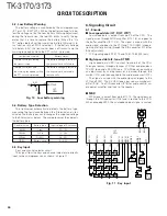
3-1. Microphone Amplifier Circuit
The signal from microphone amplified by IC13 (1/2) and
limited by AGC circuit composed of D30, D31, Q25 and Q26,
and goes through mute switch (Q30). IC13 is composed of
high-pass filter, low-pass filter and pre-emphasis/IDC circuit.
The signal enters the summing amplifier consisting of
IC12 (2/2), and passes through the D/A converter (IC16) for
the maximum deviation adjustment, and is mixed with the
low speed data from the CPU (IC7).
The output signal from the D/A converter goes to the VCO
modulation input. The other output signal from the D/A con-
verter passes through the D/A converter (IC16) again for the
BAL adjustment, and the buffer amplifier (IC17), and goes to
the TCXO modulation input.
SP
Q22
SW
IC16
VOL
IC18
AF PA
Q23,24,27
SW
SW
Q28,35
IC5
Shift register
2-tone
IC15
BPF & Compalater
CLK, DATA,STD, LOADN
IC10
IF AMP
IC11
LPF
IC13
AQUA-L
IC701
FM IF
SIGNAL
DTMF
ANSQL
IC7
CPU
LSDI
QT/DQT
HSDI
AM2
AM1
Fig. 4
Audio amplifier and squelch circuit
MIC
Q30
IC13
(1/2)
AMP
IC12
(2/2)
SUM
AMP
IC17
X701
BUFF
AMP
TCXO
VCO
AGC
SW
AQUA-L
IC13
IC16
D30,31
Q25,26
D/A
O2
I2
IC16
D/A
O8
I8
LSD
OUT
MMUTE
Fig. 5
Microphone amplifier
3-2. Drive and Final Amplifier Circuit
The signal from the T/R switch (D516 is on) is amplified by
the pre-drive (Q602) and drive amplifier (Q603) to 50mW.
The output of the drive amplifier is amplified by the RF
final amplifier (Q604) to 4.0W (1W when the power is low).
The RF final amplifier consists of two MOS FET stages.
The output of the RF final amplifier is then passed through
the harmonic filter (LPF) and antenna switch (D604 and D605)
and applied to the antenna terminal.
3-3. APC Circuit
The APC circuit always monitors the current flowing
through the RF power amplifier (Q604) and keeps a constant
current. The voltage drop at R621, R623 and R629 is caused
by the current flowing through the RF final amplifier and this
voltage is applied to the differential amplifier IC601(1/2).
IC601(2/2) compares the output voltage of IC601(1/2) with
the reference voltage from IC7. The output of IC601(2/2)
controls the VG of the RF power amplifier, drive amplifier and
pre-drive amplifier to make both voltages the same.
The change of power high/low is carried out by the change
of the reference voltage.
From
T/R SW
(D516)
Pre-
DRIVE
AMP
DRIVE
AMP
Q602
Q603
RF
AMP
Q601
RF
FINAL
AMP
Q604
ANT
SW
LPF
D604,605
ANT
VDD
VG
IC601
(1/2)
IC601
(2/2)
R621
R623
R629
+B
PC
(IC7)
Fig. 6
Drive and final amplifier and APC circuit
CIRCUIT DESCRIPTION


