MDX-G1
9
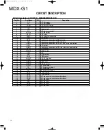
CIRCUIT DESCRIPTION
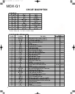
Port No.
Port Name
I/O
Description
Active
H
L
38
EEP SDA
-
Unused.
39
EEP SCL
-
Unused.
40
NC
-
Unused.
41
NC(EPM)
-
Unused.
42~45
NC
-
Unused.
46
(CE)
-
Unused.
47
LED STBY
O
Standby led (red) control port.
ON
OFF
48
LED TIMER
O
Timer led (green) control port.
ON
OFF
49
FL RESET
O
Reset output to FL dot driver.
Reset
50
FL CE
O
CE output to FL dot driver.
51
CD ON/OFF
O
CD DSP power on/off control.
ON
OFF
52~61
NC
-
Unused.
62
VCC(BU)
-
Supply power input (+5V).
63
NC
-
Unused.
64
VSS
-
Connected to ground.
65
NC
-
Unused.
66
POWER
O
Power relay control.
67~80
NC
-
Unused.
81
ST
I
Stereo detector input.
82
SD
I
SD detector input.
83
PLL CLK
O
PLL IC clock output.
84
PLL DATA
O
PLL IC data output.
85
PLL CE
O
PLL IC chip enable output.
86
PLL DO
I
PLL IC data input.
87~90
NC
-
Unused.
91
CD PROTECT
I
Detection port for CD protection.
Protection ON : Less than 4.0V
92
PROTECT
I
Detection port for power supply protection.
Protection ON : Less than 0.5V
93,94
KEY2,KEY1
I
A/D key (1,2) input.
95
TYPE
I
Discrimination of tuner destination.
96
AVSS
-
Connected to ground.
97
NC
-
Unused.
-
A/D reference voltage input for the A/D converter.
-
A/D converter positive voltage.
O
Chip enable output to electric volume system IC.
www. xiaoyu163. com
QQ 376315150
9
9
2
8
9
4
2
9
8
TEL 13942296513
9
9
2
8
9
4
2
9
8
0
5
1
5
1
3
6
7
3
Q
Q
TEL 13942296513 QQ 376315150 892498299
TEL 13942296513 QQ 376315150 892498299


