background image

(No.WA001<Rev.001>)13/18

z

Tuner Test Mode Specification

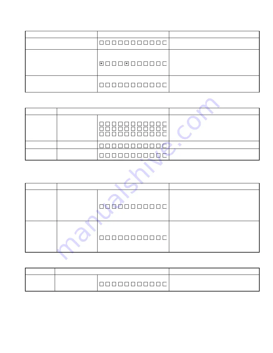
The following display shall be indicated according to the TUNER status.

‹

Operations

‹

TUNER Setting Adjustment Mode

1. Operation

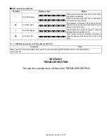
2. Operation in AUTO Adjustment Mode

Status

Display content

Details

TUNER IC Normal Error

Communication to TUNER IC not available (indi-
cated unless the mode is in Clock Display Mode). 

Adjustment not implemented

For models that TUNER adjustment is necessary
but not done (adjustment value: 0x00 or 0xFF), the
following TUNER Test Mode functions are valid
(“

ERR

”display is continuing).

Display “

ERR

“ blinks with 250ms interval.

RDS Specified data reception

Turn OFF P-CON forcibly if PS=RDS TEST is re-
ceived.
P-CON recovers with Power OFF/ON.

T

U

N

C

O

N

N

G

E

R

R

A

A

9

7

9

D

R

S

S

T

T

E

Operation

Display content

Details

SEARCH

S meter voltage judg-
ment display 

S meter value xx: Current S meter value
Determination result
OK: Within S meter voltage spec
NG: Out of S meter voltage spec

- - : No LEVEL OFFSET adjustment

ACCENT

TUNER IC display

Display TUNER IC version

BAND

BAND switch 
operation 

Execute Band Switch as shown in the following ta-
ble every time Band key is pressed in each type. 

M

S

T

x :

x

O

R

K

M

S

T

x :

x

N

R

G

M

S

T

x :

x

R

T

A

O

M

D

S

R

M

F

1

3

7

9

9

A

A

Operation

Display content

Details

„

DISP

Shift to TUNER 
setting mode 

Shift to TUNER setting mode after switching to
98.3MHz
SG setting values
Frequency: 98.3MHz, Modulation frequency:
1kHz, Modulation mode: MONO, Modulation:
OFF, Deviation: 40kHz, ANT input level: 34dBpV

„

BAND

(Toggle)

AUTO Adjustment 
Mode 

Select TUNER adjustment method (AUTO) using
BAND key.
S-xx: Current S meter value (Hex)
L-xx: Level offset value (Hex)

In case that the level offset value is not adjusted

(0xFF or 0x00), display "- -". 

S

A

x

x

x

L

x
Operation

Display content

Details

VOL PUSH

Adjustment start

Start adjustment (Start Auto adjustment, and tran-
sit to Success/Failure display depending on the
adjustment result)

S

A

x

x

x

L

x

Summary of Contents for KDC-152

Page 1: ...er This product complies with the RoHS directive for the European market M sleeve assy DC cord Remocon unit RC 405 QAL1303 001 GE34826 001A QAM1335 001 Tap screw 2x8 Screw set Trim plate QYSPSF2008MA GE40536 001A GE40578 001A x2 GE20274 001A KDC 152 KDC 153 KDC 153S Y33 3370 27 Y33 3350 13 Y33 3370 28 TDF 1215D TDF 153 TDF 153S Tuner setting adjustment after replacing E2PROM After replacing E2PROM...

Page 2: ...pm 200 rpm CLV Wow Flutter Below Measurable Limit Frequency response 1 dB 20 Hz 20 kHz Total harmonic distortion 1 kHz 0 01 Signal to Noise ratio 1 kHz 105 dB Dynamic range 90 dB MP3 decode Compliant with MPEG 1 2 Audio Layer 3 WMA decode Compliant with Windows Media Audio Audio section Maximum output power 50 W 4 Full bandwidth power at less than 1 THD 22 W 4 Speaker impedance 4 Ω 8 Ω Tone action...

Page 3: ...le sensitivity S N 20 dB MW 31 dBµ 36 µV SW 32 dBµ 40 µV CD player section Laser diode GaAIAs Digital filter D A 8 Times Over Sampling D A converter 24 Bit Spindle speed 500 rpm 200 rpm CLV Wow Flutter Below Measurable Limit Frequency response 1 dB 20 Hz 20 kHz Total harmonic distortion 1 kHz 0 01 Signal to Noise ratio 1 kHz 105 dB Dynamic range 90 dB Audio section Maximum output power 50 W 4 Full...

Page 4: ...one jack control shafts etc to be sure the product is safe to operate without danger of electrical shock Do not use a line isolation transformer during this check Plug the AC line cord directly into the AC outlet Using a Leakage Current Tester measure the leakage current from each exposed metal parts of the cabinet particular ly any exposed metal part having a return path to the chassis to a known...

Page 5: ... to check the condition of the laser diode in the optical pickup The tester s internal power source can easily destroy the laser diode 1 6 Handling the traverse unit optical pickup 1 Do not subject the traverse unit optical pickup to strong shocks as it is a sensitive complex unit 2 Cut off the shorted part of the flexible cable using nippers etc after replacing the optical pickup For specific det...

Page 6: ...n and inter lock failed or defeated Avoid direct exposure to beam 4 CAUTION This laser product uses visible and or invisible laser radiation and is equipped with safety switches which prevent emission of radiation when the drawer is open and the safety interlocks have failed or are defeated It is dangerous to defeat the safety switches 5 CAUTION If safety switches malfunction the laser is able to ...

Page 7: ...taching the Rear bracket See Fig 3 Fig 3 2 Remove the 2 screws B attaching both sides of the Top chassis See Fig 4 Fig 4 3 Remove the 3 screws C attaching the Electric unit See Fig 5 4 Disconnect the board to board connector CN502 connect ing the Electric unit and the CD mechanism See Fig 5 Fig 5 3 1 4 Removing the CD mechanism See Fig 6 1 Remove the 3 screws J attaching the CD mechanism Fig 6 3 1...

Page 8: ...3 4 Remove the two screws A attaching the Mecha control board See Fig 3 Fig 3 3 2 2 Removing the Traverse mechanism See Fig 4 5 1 Remove the five springs from the traverse mechanism See Fig 4 Fig 4 2 Remove the three screws B attaching the bottom frame as sembly See Fig 5 3 Remove the three dumpers from the bottom frame assem bly See Fig 5 Fig 5 3 2 3 Removing the Pickup See Fig 6 7 1 Remove the t...

Page 9: ...Fig 7 3 2 4 Removing the Spindle motor See Fig 8 9 1 Remove the HC CL Spring from the HC CL base and the TM base and then lift up the HC CL base See Fig 8 Fig 8 2 Remove the HC CL base from the holes on the TM base See Fig 9 Fig 9 3 Remove the two screws D attaching the spindle motor See Fig 10 Fig 10 shaft SIDE VIEW HC CL spring D ...

Page 10: ...ing motor 1 Remove the roller arm assembly from the bottom frame as sembly See Fig 11 Fig 11 2 Remove the two screws E attaching the loading motor as sembly and then remove the loading motor assembly in the direction of the arrow See Fig 12 Fig 12 E ...

Page 11: ...llowing ACCENT SEARCH RETURN VOL KDC 152 Test Mode name Operation Production Test Mode Press and hold 1 key and 3 key and reset Service Test Mode In the STANDBY source while pressing and holding 2 key press 6 key for 7 seconds Starting to press 2 key and 6 key at the same time can not be entered into the mode DC Error Information Mode Press and hold 3 key and 6 key and reset Details Difference in ...

Page 12: ... when another operation is executed The display will blink if sub clock is not functioning P R O T T E S Operation Display content Details 1 Toggle Syscom version display Syscom version Refer to Syscom Version Table All lights ON All lights ON Switch with other display 2 Toggle Serial No display Serial No display 8 digit Display as it is in hex All lights ON All lights ON Switch with other display...

Page 13: ...t S meter value Determination result OK Within S meter voltage spec NG Out of S meter voltage spec No LEVEL OFFSET adjustment ACCENT TUNER IC display Display TUNER IC version BAND BAND switch operation Execute Band Switch as shown in the following ta ble every time Band key is pressed in each type M S T x x O R K M S T x x N R G M S T x x R T A O M D S R M F 1 3 7 9 9 A A Operation Display content...

Page 14: ...9 Default for Display mode Play time Operation Display content Details Special track up Pressed Track up depend on different cases Case 1 Track 23 No 9 No 15 No 10 No 22 No 12 No 13 No 14 No 9 Case 2 Track 8 No 1 No 2 No 3 Until Last Track Case 3 8 Track 22 No 9 No 15 No 10 Until Last Track Special track down One by one Track down by sequence follow Track No 1 Toggle HC1 2 Judgement Information Di...

Page 15: ... Version Micom 3 Power ON duration display 00 50 are displayed in xx For less than 1 hour the display is indicated per 10 minutes 00001 10922 are displayed in xxxxx MAX 10922 hours 4 Disc action duration display 0 50 are displayed in xx For less than 1 hour the display is indicated per 10 minutes 00001 10922 are displayed in xxxxx MAX 10922 hours 5 Disc Eject number of times display Display Disc E...

Page 16: ...mbers of errors when there is none CD time code error count information display count skip CD time code error count information count skip mode display CD DA error count numbers xx numbers of errors and when there is none CD ROM compressed file error count numbers xx numbers of errors and when there is none CD time code error count information display no count update CD time code error count infor...

Page 17: ...on duration is not detected 1 DC ERR1 clear Clear detection information when wrong connec tion DC error in other detection duration is dis played Clear data fl ash 2 DC ERR2 display Display detecting number of times in capacitor leakage detection duration 0 4 2 DC ERR2 clear Clear number of times for detection information in capacitor leakage detection duration Clear data flash D C 1 E R R D C 1 O...

Page 18: ... No WA001 Rev 001 VSE Printed in Japan JVC KENWOOD Corporation Car Electronics Business Group 2967 3 Ishikawa machi Hachioji shi Tokyo 192 8525 Japan ...

Page 19: ...PARTS LIST CD RECEIVER KDC 152 KDC 153 KDC 153S No WA001 Rev 001 1 12 ...

Page 20: ... No WA001 Rev 001 2 12 ...

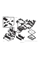
Page 21: ...255 254 253 252 251 247 240 239 238 226 223 222 221 217 216 205 J 204 202 x2 703 772 771 X16 772 731 X34 793 X34 792 X34 794 732 x2 x2 X34 Parts with the exploded numbers larger than 700 are not supplied Block No 200 EXPLODED VIEW UNIT created date 2011 09 29 No WA001 No WA001 Rev 001 3 12 ...

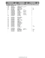
Page 22: ...AP SCREW M2 6 x 10mm 3 202 GE10283 001A TOP CHASSIS 1 204 GE10286 001A REAR COVER 1 205 GE20271 001A BOTTOM COVER 1 216 GE10290 001A LIGHT GUIDE AUX 1 217 GE20274 001A TRIM PLATE 1 221 GE34045 001A LOCK LEVER 1 222 GE34046 001A RELEASE LEVER 1 223 GE40578 001A HOOK 2 226 GE34058 001A CONDUCT RUBBER 1 238 GE40504 001A T SPRING 1 239 GE40505 001A COMP SPRING 1 240 GE40505 002A SPRING 1 247 GE34826 0...

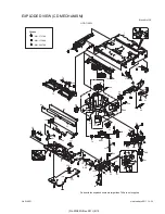
Page 23: ...8 43 42 41 39 38 37 33 32 29 27 26 24 23 22 22 21 17 16 14 13 12 2 1 902 901 903 896 834 892 804 X32 896 882 Grease W01 1738 08 W01 2007 08 W01 1737 08 HCS 1100W EXPLODED VIEW CD MECHANISM Block No 130 Parts with the exploded numbers larger than 700 are not supplied created date 2011 10 20 No WA001 No WA001 Rev 001 5 12 ...

Page 24: ...NG 1 64 LV45418 501A R ARM SPRING 1 67 LV45421 501A HC CL SPRING 1 68 LV45422 501A SUS SPRING F 1 69 LV45423 501A SUS SPRING B 2 71 LV45505 502A SW ACT SPRING 2 76 LV11689 501A DISC GUIDE 1 77 LV22828 501A FEED BRACKET 1 78 LV36813 501A SUB GUIDE CAP 1 79 LV36819 502A CLAMPER 1 81 LV38954 501A R ARM GUIDE 1 83 LV45648 501A RA COLLAR2 1 SWITCH UNIT X16 703x xx X16 IC601 BU9755KV X IC MOS 1 IC602 KS...

Page 25: ...20Ω 1 8W J 1 R659 NRS181J 561X MG RESISTOR 560Ω 1 8W J 1 K3 M8 R659 NRS181J 471X MG RESISTOR 470Ω 1 8W J 1 M9 R669 NRS181J 821X MG RESISTOR 820Ω 1 8W J 1 R670 NRS181J 821X MG RESISTOR 820Ω 1 8W J 1 K3 M8 R670 NRS181J 471X MG RESISTOR 470Ω 1 8W J 1 M9 R671 NRS181J 821X MG RESISTOR 820Ω 1 8W J 1 K3 M8 R671 NRS181J 471X MG RESISTOR 470Ω 1 8W J 1 M9 R672 NRSA63J 0R0X MG RESISTOR 0Ω 1 10W J 1 K3 M8 R67...

Page 26: ...470pF 50V J 1 C26 NCB31HK 472X C CAPACITOR 4700pF 50V K 1 K3 C26 NCB31CK 104X C CAPACITOR 0 1uF 16V 1 M9 M8 C100 NCB31AK 105X C CAPACITOR 1uF 10V K 1 C102 NCB31AK 105X C CAPACITOR 1uF 10V K 1 C103 NCB31CK 104X C CAPACITOR 0 1uF 16V 1 C110 NCB31AK 105X C CAPACITOR 1uF 10V K 1 C161 NCB31AK 105X C CAPACITOR 1uF 10V K 1 C162 NCB31AK 105X C CAPACITOR 1uF 10V K 1 C163 QEKJ1HM 475Z E CAPACITOR 4 7uF 50V ...

Page 27: ...R 0 1uF 16V 1 C713 NCB31HK 103X C CAPACITOR 0 01uF 50V K 1 C715 QERF0JM 337Z E CAPACITOR 330uF 6 3V M 1 C760 NCB31CK 104X C CAPACITOR 0 1uF 16V 1 C761 NCB31CK 104X C CAPACITOR 0 1uF 16V 1 C771 NCB31HK 472X C CAPACITOR 4700pF 50V K 1 C890 NCB31HK 104X C CAPACITOR 0 1uF 50V K 1 C901 QEZ0934 338 E CAPACITOR 3300uF 1 C902 QEKJ1CM 226Z E CAPACITOR 22uF 16V M 1 C903 QEKJ1CM 476Z E CAPACITOR 47uF 16V M 1...

Page 28: ...1 10W J 1 R527 NRSA63J 0R0X MG RESISTOR 0Ω 1 10W J 1 R528 NRS181J 0R0X MG RESISTOR 0Ω 1 8W J 1 R529 NRSA63J 0R0X MG RESISTOR 0Ω 1 10W J 1 R530 NRSA63J 103X MG RESISTOR 10kΩ 1 16W J 1 R531 NRSA63J 0R0X MG RESISTOR 0Ω 1 10W J 1 R532 NRS181J 0R0X MG RESISTOR 0Ω 1 8W J 1 R540 NRSA63J 221X MG RESISTOR 220Ω 1 16W J 1 R541 NRSA63J 0R0X MG RESISTOR 0Ω 1 10W J 1 R543 NRSA63J 0R0X MG RESISTOR 0Ω 1 10W J 1 R...

Page 29: ... R766 NRS125J 150X MG RESISTOR 15Ω 1 2W J 1 R768 NRSA63J 102X MG RESISTOR 1kΩ 1 16W J 1 R771 NRS181J 221X MG RESISTOR 220Ω 1 8W J 1 R772 NRS181J 221X MG RESISTOR 220Ω 1 8W J 1 R773 NRS181J 0R0X MG RESISTOR 0Ω 1 8W J 1 R774 NRS181J 0R0X MG RESISTOR 0Ω 1 8W J 1 R775 NRSA63J 0R0X MG RESISTOR 0Ω 1 10W J 1 R776 NRS181J 0R0X MG RESISTOR 0Ω 1 8W J 1 R778 NRSA63J 104X MG RESISTOR 100kΩ 1 16W J 1 R779 NRSA...

Page 30: ... 001 CHOKE COIL 1 CN502 QGF1040F1 26 CONNECTOR FFC FPC 1 26 1 CN701 QGZ1102J1 20 CONNECTOR 1 20 1 CN901 QNZ0607 001 CAR CONNECTOR 1 J1 QNB0190 001 ANT TERMINAL 1 J321 QNN0864 001 PIN JACK 1 S701 QSW0648 001Z TACT SWITCH 1 X1 QAX0952 001Z CRYSTAL 1 X540 QAX0929 001Z C RESONATOR 1 X701 QAX0955 001Z C RESONATOR 1 X702 QAX0401 001 CRYSTAL 32 768KHz 1 No WA001 Rev 001 12 12 ...

Page 31: ...SCHEMATIC DIAGRAMS CD RECEIVER KDC 152 KDC 153 KDC 153S No WA001 Rev 001 1 13 ...

Page 32: ... No WA001 Rev 001 2 13 ...

Page 33: ...section 3 3V 1 5V VDD5V VDD5V 1 5V IC540 VDDM1 D782 REAR SUB WOOFER OUT X540 16 934MHz X1 4MHz X701 10MHz SP FEED LOAD FOCUS TRK FWD REV DRVMUTE BTL_DMO BTL_FMO BTL_FOO BTL_TRO MUTE AMP_MUTE MUTE CD PICK UP VF1 VF2 VT1 VT2 MD LD Vc VREF TRK FOCUS FOCUS TRACKING COIL PICK UP CD Mechanism section CN502 SW1 SW2 SW3 X702 32 768kHz AMP_STBY STBY PON_PANEL SW Panel section CD servo control section CTRL1...

Page 34: ... 47k R970 10k R971 20k R973 47k R974 68K R891 0 R102 4 7k R903 1 5M R901 OPEN R301 R1 R304 R706 R704 47 R7 47 R8 4 7k R782 0 R166 4 7k R783 10k R167 100 R757 2 2k R163 12K R893 R736 47k R110 47k R100 0 R11 10K R758 10 R303 330 R781 47k R302 220 R164 220 R165 R702 47k R701 22k R341 22k R351 470 R101 220 R10 220 R9 4 7k R4 Q902 RT1N441C X Q701 RT1N241C X RT1P144C X Q972 Q702 RT1P241C X RT1P241C X Q7...

Page 35: ...MAX 76 PDo 75 VDDM1 74 SRAMSTB 73 VSS 1 72 VDD 1 71 TEST 70 RST 69 MS 68 CCE 67 BUCK 66 BUS3 65 BUS2 64 BUS1 63 BUS0 62 VDD3 61 Pio7 60 Pio6 59 Pio5 58 Pio4 57 Pio3 56 Pio2 55 Pio1 54 Pio0 53 VSS 2 52 VDD1 2 51 XVDD3 50 Xo 49 Xi 48 XVSS3 47 DVSS3L 46 Lo 45 DVDD3L 44 DVDD3R 43 Ro 42 DVSS3R 41 CDMoN3 40 Pio14 CDMoN2 39 Pio13 CDMoN1 38 Pio12 CDMoN0 FGiN 37 Pio11 36 Pio10 35 Pio9 34 Pio8 33 VDD1 3 32 ...

Page 36: ...4 S23 S22 S21 S20 S19 S18 S17 S1 S2 S3 S4 S5 S6 S7 S8 S9 S10 S11 S12 S13 S14 S15 S16 S609 S605 S608 S607 S614 S613 S606 S612 S604 7 6 5 4 3 2 1 QSW1288 001 EN601 NSW0326 001X S603 NSW0326 001X S616 NSW0326 001X S615 NSW0326 001X S610 NSW0326 001X S611 NSW0326 001X S602 0 R632 1 8W R659 1 8W R653 R620 1 8W R670 1 8W R657 0 R676 0 R677 1 8W R656 0 R622 0 R675 1 8W 1 5k R650 1 8W 820 R658 1 8W R652 1...

Page 37: ...R LOAD FEED SPINDLE LOADING LOADING GND FEED TRACKING FOCUS GND VREF Vc VF1 VT2 VF2 SW GND SW2 TR LD LD SW1 SW2 SW3 VT2 VCC LO VT1 VC MD VF2 REST VF1 LO FO SP FO FE FE TR SP SW1 SW3 TR TR FO FO MD VF1 VC VT1 VT2 VCC VF2 LO LO FE FE REST SP SP SW4 MGND FE FE LO SP SP LO REST SL1 SL2 NSW0291 001X SW2 NSW0291 001X SW3 1 3 NSW0291 001X SW1 R1 130 B1 0 26 25 24 23 22 21 20 19 18 17 16 15 14 13 12 11 10...

Page 38: ...0 C506 B529 B709 B711 B705 B704 B719 B730 B180 B110 B111 B112 B911 B909 B504 B505 B908 B716 B715 B713 B725 B726 B906 B905 B891 B904 B318 B3 B880 B315 B731 B314 B903 B313 B178 B850 B307 B308 B309 B312 B310 B306 B305 B941 B902 B552 B509 B516 B518 B519 B717 CN502 B113 B503 X540 B701 B712 B502 B901 B2 C909 B301 IC301 C304 N C303 N C302 N C301 N C9 B164 B320 CN701 C715 B727 C330 C320 C881 C907 C931 C30...

Page 39: ... R892 Q972 R909 R908 R121 C123 D111 R307 R309 R306 IC301 IC701 C304 C303 C302 C301 R762 R761 R130 R120 C131 C121 C102 D121 D120 D131 C120 C122 C130 R907 R906 Q901 L10 D890 R972 D100 D101 C9 R738 C704 R734 R752 R751 R750 R749 R748 R747 R746 R745 R725 R723 R742 C707 R709 C771 R772 R771 R737 R735 R703 R730 R729 R728 R727 R712 R721 C172 C173 C174 R768 D704 C760 C761 CN701 R733 R732 R731 IC771 C715 R71...

Page 40: ...4 R653 D657 C641 D680 MARK UL D679 D656 D655 D654 D653 D652 D651 EN601 D665 D666 D663 D662 D661 D660 D664 R652 R651 R673 D659 D674 D675 D676 D677 R672 D669 D673 S616 D658 IC602 D678 J602 S613 S615 S614 S612 S610 S611 S609 S608 S607 S606 S605 S604 S603 S602 created date 2011 09 29 No WA001 No WA001 Rev 001 10 13 ...

Page 41: ...3 C614 C615 C616 R611 R614 R612 R622 C621 R621 C642 R677 R676 R675 C671 C672 D602 R674 D603 D601 D606 D604 D605 D607 D608 L601 IC601 TL624 TL623 TL622 TL621 TL625 TL626 TL627 TL628 TL629 EN601 R631 C631 R632 IC602 CN601 J602 SWITCH UNIT X16 703x xx GEB10298 001B created date 2011 09 29 No WA001 No WA001 Rev 001 11 13 ...

Page 42: ...SW3 WHT LO YEL LO REST ORG ORG MGND WHT FE SP SP RED BLK YEL FE R1 B1 CN102 A1 LVA11003 MARK UL SW1 SW3 SW2 C N 1 0 2 B1 R1 CN101 CD PLAYER UNIT 1 X32 6530 00 LVB11003 003A created date 2011 09 29 No WA001 No WA001 Rev 001 12 13 ...

Page 43: ...PbF LVA11003 A2 P3A SW4 CD PLAYER UNIT 2 X32 6530 00 LVB11003 003A created date 2011 09 29 No WA001 No WA001 Rev 001 13 13 ...

Reviews: