8
KAC-PS4D/X4R
CIRCUIT DESCRIPTION
ISO A
RCA IN AL
VR
AMP
SE to DIF
ADC Ach
DSP
DRIVER
PWR FET
FILTER
FEEDBACK, DPSC, ADCS
OVERCURRENT DETECTION
SP OUT AL
L/R
DAC
RCA OUT
L/R
+HV REG
HV REG
LC
FILTER
FUSE
GND
BATT14.4V
OC DET
DRIVER
U-PUMP
DRIVER
FF
IC101
Q112
D107
D103
D101
D115
Q101
Q103
D105
D117
Q107
Q111
Q109
Q105
D112
D109
Q113
390
R111
R105 4.7
0.1
C129
1
C105
0.1
10K
R103
VCC
OUTB
NC8
OUTA
2
GND
3
INB
4
INA
1
NC1
7
6
5
8
0.1
C103
C101
R101
10K
C111 0.47
0.033
TP185
33
C113
120nH
R147 39
L103
R145 39
1/2W
1/2W
220u50
R107
TP184
TP180
C109
0.47
C107
1.2K
15uH
L101
1.5K
R121
47K
R137
2K
R123
390
R117
10K
R125
1
C119
1W
TP172
0.022
R109
47K
47K
R138
10K
R139
100P
C139
0.022
TP171
C121
C123
0.1
3300P
R140
C125
R113
+3.3V
+HV
FD-BL
BL
+12V
+HV
+3.3V
HV
R119 4.7K
HV
HV
+HV
+HV
+3.3V
HV
1W
R149
0.027
TH103
22K
R153
4700P
C117
C115 4700P
1.2K
R115
TH101
22K
R151
1/2W
R93
R127
100P
C63
82
1/2W
82
100P
C65
82
R128
R95
82
1/2W
1/2W
+
12
●
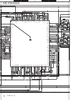
Flow of PS4D/X4R signal line and power supply
controls
• Block diagram
The signal from the pin jack is converted into the differential
signal via the isolation amplifi er, variable resistor, and single
end.
It is converted into the digital signal in the AD converter and
it is signal-conditioned in the DSP so that it can be amplifi ed
by the PWM digital amplifi er.
It is PWM-amplifi ed to the analog signal by the driver and
power MOSFET to the level that can be output from the
speaker.
●
Main signal amplifi er circuit with PWM
• Main signal amplifi er circuit with PWM
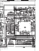
The audio signal that is DA-converted is converted into the
signal for PWM in the DSP.
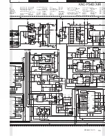
Its level is shifted in the IC101 and it is converted into the
PWM signal whose amplitude is +/- B. The “+” side of the
amplitude is controlled by Q101 of the PchMOSFET and the
“-” side is controlled by Q103 of the NchMOSFET.
The signal right after this step is converted into the digital
signal in the AD converter and is feed-backed to the DSP.
The main signal is output from SP via the low pass filter.
In addition, current of the main signal is monitored in the
over current detection circuit and when the over current is
detected the output level is controlled by the DSP.
The signal for pre-out is output to the pin jack via the DA
converter used for the pre-out.
The 14V of the battery is converted to +/-40V in the SW
regulator. The voltage is controlled in the feed-forward and
anti-pumping circuits.
Over current is detected by R109 and R149. The signal level
is lowered in the DSP when the over current is detected.
Q107 is used to detect the “+” side of the switching current
and Q105 is used to detect the “-” side of the current.


