background image

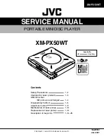
XM-PX50WT

1-4

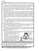
The laser diode in the traverse unit (optical pick up) is easy to be destroyed  by clothes and the human body 
 to the electrified static electricity.
Please note the explosion by static electricity when repairing.

In the equipment which uses an optical pick up (laser diode), an optical pick up is destroyed by the static 
electricity of the work environment. 
Please do the earth processing and work.

2. About the earth processing for the electrostatic destruction prevention

1)  Earth of work stand
Please pull the conductive material (conductive sheet) or the iron plate to the depository 
place of the traverse unit (optical pick up), and take the earth to ground.
2)  Human body earth
          Please use the anti-static wrist strap to exhaust the electrified static electricity to the human body.

3.    Handling the optical pick up

1) Please return according to a correct procedure based on short processing after exchanging
    parts. 
2) Do not use a tester to check the condition of the laser diode in the optical pick up .The tester 's internal
    power source can easily destroy the laser diode. 

4.  Attention when unit is disassembled

Please refer to "Disassembling method" for how to detach .

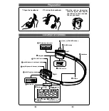
Conductive material (conductive 
sheet) or the iron plate

anti-static wrist strap

Attention when MD pickup is exchanged

1.  About the static electricity protection measures

Solder short

1) Please be sure to solder before a flexible wire is removed from connector on a main printed 
    circuit board as shown. 
    if you removes without soldering.the MD picking up assembly might destroy
2) When installing , solder in the part of short round should be removed after a flexible wire is connected with 
    connector.

Summary of Contents for XM-PX50WT

Page 1: ...TD XM PX50WT XM PX50WT Area Suffix UB Hong Kong Contents Safety Precautions Important for laser products Attention when MD pick up is exchanged Disassembly method Adjustment method Maintenance of laser pickup Replacement of laser pickup Description of major ICs 1 2 1 3 1 4 1 5 1 11 1 12 1 12 1 13 25 ...

Page 2: ...urrnet check Electrical shock hazard testing After re assembling the product always perform an isolation check on the exposed metal parts of the product antenna terminals knobs metal cabinet screw heads headphone jack control shafts etc to be sure the product is safe to operate without danger of electrical shock Do not use a line isolation transformer during this check Plug the AC line cord direct...

Page 3: ...g laserstrålning är denna del är öppnad och spårren är urkopplad Betrakta ej strålen VARO Avattaessa ja suojalukitus ohitettaessa olet alttiina näkymättömälle lasersäteilylle Älä katso säteeseen ADVARSEL Usynlig laserstråling ved åbning når sikkerhedsafbrydere er ude af funktion Undgå udsættelse for stråling ADVARSEL Usynlig laserstråling ved åpning når sikkerhetsbryteren er avslott unngå utsettel...

Page 4: ...ust the electrified static electricity to the human body 3 Handling the optical pick up 1 Please return according to a correct procedure based on short processing after exchanging parts 2 Do not use a tester to check the condition of the laser diode in the optical pick up The tester s internal power source can easily destroy the laser diode 4 Attention when unit is disassembled Please refer to Dis...

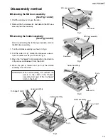
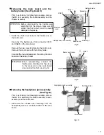
Page 5: ...bly as shown in Fig 4 Move the U shaped notch marked b in the direction of the arrow and release it from the shaft Move the part c inward and pull out the Holder assembly from the shaft 1 2 3 4 Removing the holder assembly See Fig 3 and 4 When reassembling first reattach the part c to the shaft of the Chassis assembly And next fit the U shaped notch to the shaft ATTENTION MD door assembly Door lev...

Page 6: ...ut the eject unit Remove the screw D E F and G attaching the chassis assembly respectively Disengage the three joints e of the bottom case and the battery holder Remove the chassis assembly and the jack cover at once 1 2 3 4 5 Removing the chassis assembly See Fig 5 to 7 Chassis assembly Side arm R Battery lid Tab d Joint e B C Eject unit C G D F E Bottom case Battery holder Joints e Battery lid C...

Page 7: ...cedures remove the MD door assembly the holder assembly chassis assembly and the main board Disconnect the flexible wire extending from the headphone jack from connector CN601 on the main board 1 When reassembling connect the flexible wire extending from the pickup to the connector on the main board and unsolder the short circuit round ATTENTION Before disconnecting the flexible wire extending fro...

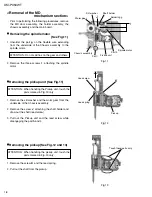
Page 8: ...p unit See Fig 11 Prior to performing the following procedures remove the MD door assembly the holder assembly the chassis assembly and the main board Removal of the MD mechanism section Do not spill flux on the gear and others ATTENTION When handling the Pickup unit touch the parts marked in Fig 13 only ATTENTION Remove the screw K and the lead spring Pull out the shaft from the pickup 1 2 Removi...

Page 9: ...der soldering k connecting the flexible wire to the feed motor Remove the two screws L attaching the feed motor 1 2 3 Removing the feed motor See Fig 14 When reassembling reattach the flexible wire with an adhesive tape and solder ATTENTION Chassis assembly Feed motor j Soldering k L Pickup unit L Fig 14 ...

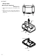
Page 10: ...om of the body Remove the top cover upward while pushing the front part a Pull out the charge board from the bottom cover 1 2 Removing the charge board See Fig 1 to 3 Charge stand Fig 1 Fig 2 Fig 3 A A A A Top cover Part a Push Charge board Bottom cover ...

Page 11: ... Indication change OK MO DISC ADJUST Pre TG Insert the Pre master disc Executes by BASS LCD Indication change Pre DISC ADJUST Executes by BASS LCD Indication change XXYYZZ Press STOP RESET Executes by BASS LCD Indication Left out the test mode power off and END Press PLAY MODE DISPLAY BASS and PLAY key together more than 3sec at power off condition VOL next item VOL before item PLAY LASER Insert t...

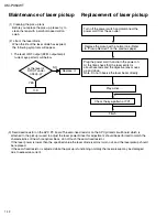
Page 12: ...life of the laser diode has expired the following symptoms will appear 1 The level of RF output EFM output ampli tude of eye pattern will below Is the level of RFOUT under 0 35Vp p Replace it NO YES O K 3 Semi fixed resistor on the APC PC board The semi fixed resistor on the APC printed circuit board which is attached to the pickup is used to adjust the laser power Since this adjustment should be ...

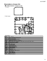
Page 13: ...ier output GND in power amplifier output steps Power amplifier output Symbol FUNCTION CC2 CC2 A B 2 2 1 ref ref CC1 CC B A B BEEP OUTA Pin no B in power amplifier output steps Smoothness of level detection of boost BST amplifier input signal level variable control by input lever to boost AGC input terminal Output terminal of BST amplifier2 Terminal NF of BST amplifier2 Output BST amplifier1 NF of ...

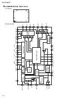
Page 14: ...OMF CPOUT CPC3 CP3 CPC2 CP2 CPC1 CP1 VCO RMAX RMIN VCOIN VCC MCLOCK CLKSEL S S BRAKE VCONT VCREF GND PGND FG2 FG SLOPE F R Controllor Timing controllor Phase Comparator 1 8 PWM VCO Full Wave Rectifilter Sensoeless Logic Charge Pump Voltage Driver Sample and Hard 1 Pin layout 2 Block diagram 1 12 36 25 37 48 24 13 ...

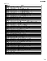
Page 15: ... maximum oscillation frequency of VCO The terminal to set minimum oscillation frequency of VCO The terminal to control oscillation frequency of VCO The terminal to select inside and outside clock The terminal to oscillation sawtooth for PWM signal The terminal to oscillation sawtooth for soft switching signal The terminal to monitor CLOCK signal The GND for the part except the power section The te...

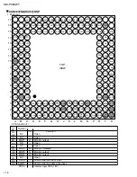
Page 16: ... RFI AVD1 MVCI PD0 A11 XOE FRDR FFDR VDC4 VSC4 SRDR FS4 SPFD SPRD SFDR TEST2 TEST1 FGIN TST2 EFM0 TEST3 VSI03 TST3 VDI03 SPCU SPDW SPDV TST4 SPCW SPCV VSC5 SLDW SLDV SLCV SLCU VDC5 BYPS TST5 SLCW DVDD1 D3 VSC3 VDC3 D0 D2 D1 XCAS IXWE A09 XRAS IXOE A07 A10 A08 DVI01 A00 VSI01 A05 A01 A06 A03 A04 A02 F256 XBCK VSC2 VDC2 DADT LRCK VDI00 TST8 ADDT MNT1 MNT0 VDC0 SENS XRST RPWR VDI OSC DVDD0 DA VDDL DA...

Page 17: ... tal osc circuit input OSC sel VDD 2 5V X tal osc circuit output Internal 16bit DRAM GND Internal 16bit DRAM GND OSC sel GND Internal DAC Lch output Internal DAC VDD Lch 2 5V Internal DAC GND Internal DAC GND VREF Lch Internal DAC VDD Rch 2 5V Internal DAC GND Rch Internal DAC Rch output Internal DAC VREF Rch Internal logic GND X tal frequency select L 45 1584MHz H 22 5792MHz Test terminal Connect...

Page 18: ...a input output Internal 16Mbit DRAM VDD Open Open External DRAM output chip enable output Open Open Open Internal 16Mbit DRAM GND External DRAM write enable output Analog PLL phase compare output Playback EFM comparator slice level input Playback EFM binarization signal output Clock input from external VCO Analog GND Playback EFM comparator bias current input Analog power supply 2 5V Filter input ...

Page 19: ...ervo drive PWM output Internal logic VDD 1 8V Internal logic GND Sled servo drive PWM output 176 4kHz clock output X tal system Spindle servo drive output Spindle servo drive output Sled servo drive PWM output Test terminal Connect to GND Test terminal Connect to GND Spindle CAV servo FG input Test terminal Open EFM output at recording Test terminal Connect to GND 2 5V I O Vss Test terminal Open 2...

Page 20: ...put Program enable Ground Power supply Not connected 1 Pin layout 3 Block diagram 2 Pin function DO EEPROM 2048bit 128 X 16 16 16 R W AMPS AND AUTO ERASE DECODER DATA REGISTER ADD BUFFER INSTRUCTION DECODE CONTROL AND CLOCK GENERATION INSTRUCTION REGISTER DI CS SK PE VREF VPP SW VPP GENERATOR Fnction VDD OUT IN Vss IN 5 4 1 2 3 1 Pin layout Block diagram TC75S51F X IC505 Ope amp ...

Page 21: ...tput terminal 21dB ope amp input terminal Serial data input terminal Shift clock input terminal Latch input terminal Stand by setting terminal F0 count setting terminal Reference voltage output terminal EQ IF setting terminal BPF3T IF setting terminal Power supply BPF3T IF setting terminal Tracking error signal output terminal Sled error signal LPF capacitor connect terminal Sled error signal outp...

Page 22: ...minal Power supply terminal Non connect VSS terminal Function Symbol Pin No 3 Block diagram 1 Pin layout 2 Pin function IC PST3421U X IC504 System reset VIN CONT GND BANDGAP REFERENCE THERMAL SENSOR Cnp VOUT VIN VOUT CONT NOISE BYPASS GND GND 6 5 4 1 2 3 TK11223BMC X IC961 Regulator 1 Pin layout 2 Block diagram ...

Page 23: ... 1 4 PS H H H H H L OE L L L L H X FI L L H H X X RI L H L H X X FO L L H L L Z RO L H L L L Z X Don t Care Z High Impedance MPC17A139MTB X IC400 4ch bridge driver Vc Vc Vc V G V G L G AGND V D1 V D1 F O1 R O1 V D2 V D2 F O2 R O2 P GND V D3 V D3 F O3 R O3 P GND V D4 V D4 F O4 R O4 P GND R GND V G V G V G Vc Vc Vc Vc CLK PS FI1 RI1 GND FI2 RI2 FI3 RI3 FI4 RI4 OE CLOCK CLK Detector DC DC Converter C...

Page 24: ...Battery voltage detect terminal Connect to temp detect GND GND Pin No Symbol Function Pin No Symbol Function ANI5 ANI6 SPSEL AVSS VADJ AVREF1 RMRX RMTX SRDT SWDT SCLK BEEP PSW MONDATA MONCLK XRST2 TG ACB TRAIN XRST XLAT LVCTL LDON RFOFF SLOFF MUTE DIR VSS1 PS SS MON1 MON2 MONXLAT GND GND Non connect GND Non connect Voltage adjust Analog reference voltage Remocon data input terminal Remocon data ou...

Page 25: ...voltage det Power supply Chip enable GND Ext Tr connect VOUT VDD CE GND EXT Symbol Function Phase Compensation Error Amp PWM Comparator Vref with Soft Start GE PWM PFM Controller Ramp Wave Generator OSC Buffer Driver VDD EXT GND VOUT CE 1 Pin layout 3 Block diagram 2 Pin function ...

Page 26: ...C601 HP AMP CN601 J101 W V U COM SLD SLD W V U COM TRK FCS PS RFI VC PEAK BOTM ABCD FE AUX1 ADFG SE T E F0CNT APCREF DTRF CKRF XLRF SPFD SPRD SPFG XBCK AOUTL AOUTR Lch Rch AOUTL AOUTR MUTE BEEP PSW CSI CSL DO DI SLCK SWDT SRAT SQSY XINT SENS MNT3 MNT0 SLOFF XLAT XRST FS4 FFDR FRDR TFDR TRDR SFDR SRDR SS XRST2 LDON RMDATA Block diagram ...

Page 27: ...30 1 1 SSM3K01F X FMMT617 X 10 6 3 0 0047 330 330 0 1 1 QGF0515F4 09X 0 NI 1 NI SI2305DS X 22 100 1 470k 10 100K 10K XC6367B101M X 0 047 CRS01 W 15k NSW0108 001X XC6367B101M X DTC144EE X DTC144EE X S 80821ANNP W 1 1 NI NI DTA144EE X DTC144EE X 0 01 2SC4081 QR X 470K DTA124XUA X 2SB1219 RS X NI 0 22 680k 1K 0 1 1 NI NI 100 100 330P 22k 330P 22k 10 6 3 0 1 DTA143TE X 22 100K 0 NI 68K 1 2K 10K 1 16 1...

Page 28: ...3 R27 R28 C11 IC1 R18 R17 C1 C4 R4 R5 R8 R9 R10 R12 R16 R15 D2 D1 C2 R1 R31 SSM3J01F X 100k 10k BA10324AF W KTB772 Y 10k 470 1k BA10324AF W 47k 220k 10k 0 068 16 220P 1k BA10324AF W LV32351 001A LV32351 001A 0 01 QNA0025 001 LV32351 001A 10k 82k 0 01 BA10324AF W 100k 1M 220 16 1 16 6 8k 10k 270k 82k 560 82 43k 100k MTZJ3 9B T2 TLSU126 T 4 7 10 0 22 120 ...

Page 29: ...C921 C924 C923 Q501 Q961 IC2 IC300 IC501 IC502 R530 IC601 IC901 R961 IC961 K602 K603 K604 R65 L402 L403 L404 L405 L501 C963 L602 C961 C962 Q60 Q61 Q300 Q301 Q901 R304 R923 Q964 Q965 R2 R3 R60 R526 C513 R112 R212 IC505 R303 R305 R306 R307 R308 R311 R314 R315 R316 R317 R318 R320 R321 R322 R323R324 R325 R326 R328 R335 R336 R337 R338 R965 R966 D501 R528 R354 R364 R371 R372 R373 R376 R377 R378 R379 R38...

Page 30: ...2 6 I H A B C D E F G 1 2 3 4 5 6 XM PX50WT XM PX50WT M E M O ...

Page 31: ...ot available as service parts Contents Exploded view of general assembly and parts list Charger assembly and parts list MD mechanism assembly and parts list Electrical parts list Packing materials and accessories parts list XM PX50WT 3 2 3 4 3 5 3 6 3 9 Area suffix UB Hong Kong ...

Page 32: ...0 38 34 42 41 41 41 33 37 36 35 39 32 31 30 25 26 29 28 27 18 1 19 15 16 17 14 13 21 23 24 22 3 20 10 4 6 5 7 12 2 8 9 11 25 A A Jack board Main board Exploded view of general assembly and parts list Block No M M M 1 ...

Page 33: ...2142 002A SHEET 1 19 LV32242 001A B CONTACT ASSY 1 20 LV32201 002A BATTERY LID 1 21 VKZ4616 008 SCREW 1 B CONTACT ASSY 22 LV42222 001A PROTECTOR 1 FOR PCB 23 LV40242 001A MINI SCREW 1 FOR PCB MECHA 24 LV30225 0A6A SPACER 1 FOR MECHA F PC 25 QYSPSGU1425M TAP SCREW 2 FOR PCB 26 LV40241 004A SPECIAL SCREW 1 FOR MECHA 27 LV31339 004A CAUTION LABEL 1 28 LV32202 001A H P JACK COVER 1 29 QYSPSGU1425M TAP...

Page 34: ... Parts name Area A Parts list Q ty Description Block No M2MM 1 LV20897 005A BOTTOM CASE 1 PC CLEAR 2 LV40243 001A FOOT 2 FOR BOTTOM 3 QYSDSF2006Z SCREW 4 BOTTOM TOP 4 LV10451 001A TOP COVER 1 PC 5 LV20898 001A INNER CABI 1 PC 6 LV32349 002A LENS 1 PMMA 7 LV32350 001A HOOK 1 POM 8 QYSDSF2006Z SCREW 1 FOR HOOK Charger ...

Page 35: ...S Y 1 2 QAR0113 001 FEED MOTOR 1 3 QYSPSFT1425M MINI SCREW 2 M1 4 PX2 5 B 5 QAL0237 001 PICK UP 1 6 LV32031 001A LEAD SPRING 1 7 QYSPSGT1425N MINI SCREW 1 M1 4 BX2 5 N 8 LV32114 001A LEAD SCREW 1 9 LV41132 001A METAL 1 10 LV41133 001A WHEEL GEAR 1 11 LV41134 003A SHAFT HOLDER 1 12 QYSPSFT1425M MINI SCREW 1 M1 4 PX2 5 B 13 QAR0112 001 SPINDLE MOTOR 1 14 QYSPSFT1425M MINI SCREW 3 M1 4 PX2 5 B 15 LV4...

Page 36: ...APACITOR C 457 NCB31HK 102X C CAPACITOR C 458 NCB31CK 473X C CAPACITOR C 459 NCB21AK 105X C CAPACITOR C 460 NCB31HK 682X C CAPACITOR C 461 NCB31CK 473X C CAPACITOR C 463 NCB21AK 105X C CAPACITOR C 500 NCB21AK 105X C CAPACITOR C 503 NCB31CK 104X C CAPACITOR C 504 NCB21AK 105X C CAPACITOR C 506 NCB31CK 104X C CAPACITOR C 507 NCB31CK 104X C CAPACITOR C 509 NCB31CK 104X C CAPACITOR C 510 NCB31HK 102X ...

Page 37: ... 369 NRSA6AJ 102W MG RESISTOR R 371 NRSA6AJ 103W MG RESISTOR R 372 NRSA6AJ 104W MG RESISTOR R 373 NRSA6AJ 684W MG RESISTOR R 376 NRSA6AJ 332W MG RESISTOR R 377 NRSA6AJ 102W MG RESISTOR R 378 NRSA6AJ 105W MG RESISTOR R 379 NRSA6AJ 102W MG RESISTOR R 380 NRSA6AJ 151W MG RESISTOR R 385 NRSA6AJ 103W MG RESISTOR R 386 NRSA6AJ 103W MG RESISTOR R 387 NRSA6AJ 103W MG RESISTOR R 388 NRSA6AJ 103W MG RESISTO...

Page 38: ...SC2412K R X TRANSISTOR Q 4 2SC2412K R X TRANSISTOR Q 5 2SC2412K R X TRANSISTOR Q 6 SSM3J01F X FET Q 7 2SC2412K R X TRANSISTOR R 1 NRZ0063 R22X MF RESISTER R 2 NRSA63J 104X MG RESISTOR R 4 NRSA63D 682X MF RESISTOR R 5 NRSA63D 103X MG RESISTER R 6 NRSA63J 473X MG RESISTOR R 7 NRSA63J 471X MG RESISTOR R 8 NRSA63D 274X MG RESISTOR R 9 NRSA63D 823X MG RESISTOR R 10 NRSA63J 561X MG RESISTOR R 11 NRSA63J...

Page 39: ...0 002A PACKING CASE 1 P 3 QPA01202505 POLY BAG 1 FOR CHARGER Item Parts number Parts name Area A Parts list Q ty Description Block No M5MM A 1 LVT0593 001A INST BOOK 1 ENG A 2 LV42298 001A 1 A 3 QAB0024 006 NI MH BATTERY 1 1400MAH A 4 LV30791 001A BATTERY CASE 1 A 5 QAL0281 001 AC ADAPTER A 1 AA R352 FOR CHA A 6 QAN0021 006 HEAD PHONE 1 A 7 QAL0252 004 REMOCON 1 A 8 LV32289 001A SOFT CASE 1 A 9 LV...

Page 40: ...nted in Japan 200101 O VICTOR COMPANY OF JAPAN LIMITED AUDIO COMMUNICATION BUSINESS DIVISION PERSONAL MOBILE NETWORK BUSINESS UNIT 10 1 1chome Ohwatari machi Maebashi city 371 8543 Japan No 20901 XM PX50WT ...

Reviews: