background image

SERVICE MANUAL

No.20872

Sep. 2000

COPYRIGHT      2000 VICTOR COMPANY OF JAPAN, LTD.

Printed in Japan
200009(S)

 No.20872

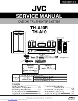
DVD DIGITAL THEATER SYSTEM

TH-A10R/TH-A10

TH-A10R/TH-A10

TH-A10R

TH-A10

XV-THA10R (DVD player)/XV-TH-A10

SP-THA10

(Speaker section)

SP-PWA10 (Powered subwoofer)
SP-XCA10 (Center speaker)

SP-XSA10 (Satellite speaker) x 4

Contents

Safety Precautions
Important for laser products
Preventing static electricity
Disassembly method
Adjustment method

Flow of functional operation
                       until TOC read
Maintenance of laser pickup
Replacement of laser pickup
Description of major ICs

1-2
1-3
1-4
1-5
1-21

1-24
1-25
1-25
1-26

Area Suffix

TH-A10R

B
EN
EE

U.K.

Northern Europe

Russia

Area Suffix

TH-A10

E

Continental Europe

VICTOR COMPANY OF JAPAN, LIMITED

OPTICAL DISC BUSINESS DIV. PERSONAL & MOBILE NETWORK BUSINESS UNIT

AV & MULTIMEDIA COMPANY 1644, Shimotsuruma, Yamato, Kanagawa 242-8514, Japan

TH-A10R

TH-A10

SP-PWA10

SP-XSA10

SP-XSA10

SP-XCA10

RM-STHA10R

XV-THA10R

RM-STHA10EC

Summary of Contents for RM-STHA10EC

Page 1: ...4 Contents Safety Precautions Important for laser products Preventing static electricity Disassembly method Adjustment method Flow of functional operation until TOC read Maintenance of laser pickup Replacement of laser pickup Description of major ICs 1 2 1 3 1 4 1 5 1 21 1 24 1 25 1 25 1 26 Area Suffix TH A10R B EN EE U K Northern Europe Russia Area Suffix TH A10 E Continental Europe TH A10R TH A1...

Page 2: ...ge currnet check Electrical shock hazard testing After re assembling the product always perform an isolation check on the exposed metal parts of the product antenna terminals knobs metal cabinet screw heads headphone jack control shafts etc to be sure the product is safe to operate without danger of electrical shock Do not use a line isolation transformer during this check Plug the AC line cord di...

Page 3: ... during transport and before installation both sides of the laser diode on the replacement optical pickup are shorted After replacement return the shorted parts to their original condition Refer to the text 2 Do not use a tester to check the condition of the laser diode in the optical pickup The tester s internal power source can easily destroy the laser diode 1 2 Handling the traverse unit optica...

Page 4: ...und the laser diode and actuator 2 Do not check the laser diode using a tester as the diode may easily be destroyed 3 It is recommended that you use a grounded soldering iron when shorting or removing the laser diode Recommended soldering iron HAKKO ESD compatible product 4 Solder the land on the optical pickup s flexible cable Note Short the land after shorting the terminal on the flexible cable ...

Page 5: ...ear cover on the back of the body Pull out the rear cover backward 1 Removing the rear cover See Fig 3 Prior to performing the following procedure remove the top cover and the rear cover Move the left side cover backward to release the five joint hooks b and remove the left side cover outward Remove the right side cover in the same way 1 2 Removing the right and left side covers See Fig 4 and 5 Di...

Page 6: ...body Remove the two screws C on the upper side of the body Remove the three screws D on the bottom of the body Release the five joints c and detach the front panel assembly toward the front 1 2 3 4 Removing the front panel assembly See Fig 6 to 9 Fig 6 Fig 7 Fig 8 Fig 9 Front panel assembly CN802 Joint c Joint c C C Joint c Front panel assembly D D Joint c Joint c Front panel assembly Front panel ...

Page 7: ...n the same way 1 2 Removing the right and left corner covers See Fig 10 and 11 Prior to performing the following procedure remove the top cover and the rear cover Remove the eighteen screws E and the one screw F attaching the rear panel Release the two joints e on both sides of the body 1 2 Removing the rear panel See Fig 12 to 14 Fig 10 Fig 11 Fig 12 Fig 12 Fig 12 Joints d Joint d Left corner cov...

Page 8: ...d wire from CN101 CN103 and CN502 of the DVD servo control board on the underside of the DVD servo control board case Remove the four screws H attaching the DVD servo control board 1 2 3 Removing the DVD servo control board See Fig 15 to 17 Fig 15 Fig 16 Fig 17 Digital I O board Analog I O board CN201 CN681 DVD servo control board case CN687 G DVD servo control board case CN501 CN503 CN502 CN103 C...

Page 9: ...moving the analog I O board the digital I O board See Fig 18 and 19 Prior to performing the following procedure remove the top cover the rear cover and the DVD servo control board case Remove the two screws E attaching the tuner board on the back of the body Disconnect connector CN111 on the tuner board from the sub board Disconnect connector CN131 on the sub board from the main board 1 2 3 Removi...

Page 10: ...to performing the following procedure remove the top cover the rear cover the front panel assembly the DVD servo control board case and the digital I O board Disconnect the harness from the spacer on the upper side of the DVD mechanism cover Remove the two screws E attaching the power board on the back of the body Disconnect the harness from connector CN911 and CN912 on the power board Remove the ...

Page 11: ...ar panel the DVD mechanism assembly the power board and the sub board Remove the four DVD spacers on the upper side of the main board Remove the five screws N attaching the main board 1 2 Removing the main board See Fig 26 Dithe harness from connector CN705 on the power switch board sconnect Remove the three screws O attaching the power switch board 1 2 Removing the power switch board See Fig 27 P...

Page 12: ... the IC board See Fig 27 Prior to performing the following procedure remove the LCD board and the IC board Disconnect the harness from connector CN705 on the power switch board Remove the two screws S attaching the LED board 1 2 Removing the LED board See Fig 27 Prior to performing the following procedure remove the LCD board Disconnect the harness from connector CN702 on the eject board Remove th...

Page 13: ... base 1 Turn the up down cam lever clockwise in the direction of the arrow in Figure 2 to lower the position of the mechanism 2 Manually set the loading tray to the fully open position 3 Stretch the tray stoppers on both sides of the loading base outward and pull out the tray Figure 1 Figure 2 Figure 3 Figure 4 Loading tray Clamper base Loading tray front side Loading base Lever Up down cam Push P...

Page 14: ...g the T mechanism unit 1 Remove the two screws at C fixing the mechanism control base from the bottom of the traverse unit 2 Pull out the CN12 connector and detach the mechanism control board 3 Remove the card wire from the CN13 connector on the mechanism control board 4 Pull out the FPC holder from the CN12 connector on the reverse side of the mechanism control board and remove the flexible harne...

Page 15: ...chanism control board 1 Remove the FPC from the feed motor connector on the turntable spindle motor board 2 Remove the two screws at E fixing the feed motor unit Removing the optical pickup unit refer to Figure 9 o Remove the traverse mechanism unit o Remove the mechanism control board o Remove the feed motor unit 1 Remove the screw at F fixing the guide shaft holder at B then simultaneously remov...

Page 16: ...G fixing the pulley gear 5 Pull out drive gear 2 then drive gear 1 Removing the loading motor board refer to Figures 11 12 o Remove the clamper base o Remove the disk tray 1 Remove the loading belt 2 Remove the two screws at H fixing the loading motor 3 Remove the screw at I and the three pawls at C fixing the loading motor base from the reverse side of the loading base Lever Loading base Up down ...

Page 17: ...ior to performing the following procedure remove the amplifier assembly Pull out the volume knob Remove the four screws B attaching the heat sink cover Remove the twenty screws C and the one screw D attaching the amplifier cover 1 2 3 Removing the heat sink cover and the amplifier cover See Fig 2 and 3 Disassembly method Fig 1 A A A A B B C C C C C C C D CN109 Fig 2 Fig 3 Amplifier assembly Amplif...

Page 18: ...body Remove the two screws C on the upper side of the body Remove the three screws D on the bottom of the body Release the five joints c and detach the front panel assembly toward the front 1 2 3 4 Removing the front panel assembly See Fig 6 to 9 Fig 6 Fig 7 Fig 8 Fig 9 Front panel assembly CN802 Joint c Joint c C C Joint c Front panel assembly D D Joint c Joint c Front panel assembly Front panel ...

Page 19: ...n the same way 1 2 Removing the right and left corner covers See Fig 10 and 11 Prior to performing the following procedure remove the top cover and the rear cover Remove the eighteen screws E and the one screw F attaching the rear panel Release the two joints e on both sides of the body 1 2 Removing the rear panel See Fig 12 to 14 Fig 10 Fig 11 Fig 12 Fig 12 Fig 12 Joints d Joint d Left corner cov...

Page 20: ...rd wire from CN101 CN103 and CN502 of the DVD servo control board on the underside of the DVD servo control board case Remove the four screws H attaching the DVD servo control board 1 2 3 Removing the DVD servo control board See Fig 15 to 17 Fig 15 Fig 16 Fig 17 Digital I O board Analog I O board CN201 CN681 DVD servo control board case CN687 G DVD servo control board case CN501 CN503 CN502 CN103 ...

Page 21: ...lization the keys may not be operated Press the POWER key to initiate the STAND BY mode and the test mode will then be cancelled Adjustment and confirmation matter 1 The oscilloscope is connected between 1 RFOP of CN104 and 2 GND 2 Reproduction of the test disc VT 501 made by JVC 3 It is confirmed that RF LEVEL is 350mVp p 150mVp p 4 When there is disorder in the waveform road cuts etc test disk i...

Page 22: ...tension cord No QUQ110 3740AM General tool Hex head wrench 1 27 mm 4 Flap adjustment of the Pick up guide shaft 1 Make sure that there is no disc on the tray 2 Press both the PLAY and OPEN CLOSE keys of the main unit to activate the primary power and Version3 Region cord will be displayed on the FL indicator Note If the FL indicator display stops and remains at TEST 0 unplug the power cord from th...

Page 23: ...nge for a new test disc and adjust optics 4 Other discs might not be able to be reproduced when adjusting on a curved disc A A B Fig 2 Point of adjustment Please execute the static electricity protection measures before starting the adjustment When the following parts are exchanged optical adjustment Adjust the flap of the disc motor is necessary 1 The disc motor was exchanged 2 The laser pick up ...

Page 24: ...shipment to match the characteristics of the optical block Do not change the setting of these half fixed resistors for laser power adjustment Destruction of Traverse Unit and Laser Pickup by Static Electricity Laser diodes are easily destroyed by static electricity charged on clothing or the human body Before repairing peripheral elements of the traverse unit or pickup be sure to take the followin...

Page 25: ...T3 LOUT3 DEM1 DEM0 MCKO DVDD DVSS PD XTS ICKS1 ICKS0 CAD1 CAD0 CDTO CDTI CCLK CS PIS XTO XTI AVSS AVDD VREFH VCOM LIN LIN RIN RIN LOUT1 ROUT1 LOUT2 ROUT2 LOUT3 ROUT3 LPF LPF LPF LPF LPF LPF DAC DAC DAC DAC DAC DAC DATT DATT DATT DATT DATT DATT ADC ADC HPF HPF Audio I F MCLK BICK LRCK SDOUT SDIN1 SDIN2 SDIN3 SDTO SDTI1 SDTI2 SDTI3 SDOS DAUX Format Converter AL4527 IC601 A D D A Converters 1 Termina...

Page 26: ... V Power down reset terminal L Power is down and register is initialized Input clock selection 2 terminals Input clock selection 1 terminals Input clock selection 0 terminals Chip address 1 terminal Chip address 0 terminal DAC3 L channel analog output terminal DAC3 R channel analog output terminal DAC2 L channel analog output terminal DAC2 R channel analog output terminal DAC1 L channel analog out...

Page 27: ...CS SK PE 1 2 3 4 PE VCC CS SK NC GND DO DI 8 7 6 5 8 PIN SOP Pin no Symbol 1 PE 2 VCC 3 CS 4 SK 5 DI 6 DO 7 GND 8 NC Function Program enable With built in pull up resistor Power supply Chip selection Cereal clock input Cereal data input Cereal data output Ground No connection NOTE The pull up resistor of the PE pin is about 2 5M VCC 5V AK93C65AF X IC403 EEPROM 1 Terminal layout 2 Block diagram 3 P...

Page 28: ...OTTOM RFENV FC BOOST OFTR BDO JITOUT GND3 FUPDN ITDLI VCOIN PLFLT PLFLT2 FCPO PCPO VCC3 CAPA DTRD IDGT VCC5 RDCKP RDCKN RDTP RDTN GND5 GND4 VCC4 DTMONN DTMONP DSLFLT DSLO FLTOUT DCFLT VREF3 VPWBDO VPWOFT IDDLY DBAL GND1 VREF1 TKCNT TKCFLT TEOUT TEI RSCL LDONB LDONA LPCOA LPC1 VHARF TGBAL POFLT PTH TBAL TG FGCTL FBAL FEOUT FEN VREFL VREFC VREFH PULIN SEN SCK STDI STNBY XTRON MTRON ROMRAM FE SSD FE ...

Page 29: ...al DSL PLL drawing mode switch terminal SEN Cereal data input terminal SCK Cereal data input terminal STDI Cereal data input terminal Standby mode control terminal Tracking OFF holding input terminal Monitor output ON OFF switch terminal ROM RAM switch terminal Standard current source terminal Tracking error output Amp reversing input terminal Tracking error signal output terminal Track count dete...

Page 30: ...output terminal OFTR output terminal Booth control terminal for filter FC control terminal for filter RF enve output terminal Bottom enve detection filter terminal Peak enve detection filter terminal AGC amplifier gain control terminal AGC amp filter terminal Sag cancellation circuit filter terminal BDO detection capacitor terminal BDO detection capacitor terminal BCA detection level setting termi...

Page 31: ...unction 15 16 17 18 19 20 21 22 23 24 25 26 27 28 VO4 VO4 VO3 VO3 PowVcc2 STBY2 GND OPOUT3 OPIN3 OPIN3 OPOUT4 OPIN4 OPIN4 PreVcc O O O O I O I I O I I Non inverted output of CH4 Inverted output of CH4 Non inverted output of CH3 Inverted output of CH3 Vcc for CH3 4 power block Input for Ch4 stand by control Substrate ground Output for CH3 OP AMP Inverting input for CH3 OP AMP Non inverting input fo...

Page 32: ...g timing shift of VD input Taking timing shift of VD input Taking edge specification of VD input 0 up 1 down Timing shift input of output data Timing shift input of output data Non connect Field Identification signal output H blanking output V blanking output Output timing setting of DOUT 0 up 1 down Power supply Field memory read data input Connect to GND Field memory read clock Field memory writ...

Page 33: ...e signal Analog brightness signal G drive signal Power supply for Y G DAC Analog chroma signal Analog chroma signal Power supply for C Cr RDAC Connect to ground for DAC Standard BIAS for DAC1 Standard voltage for DAC1 Power supply for DAC Standard voltage for DAC2 Standard BIAS for DAC2 Non connect Analog composite drive signal Analog composite drive signal Power supply for CVBS Cb B DAC2 Analog b...

Page 34: ... inout AD 10 Key input 1 5 10 Key input 6 10 10 B Apply 5V B Apply 5V 10MHz OSC 10MHz OSC GND Unused Connects with GND Unused Connects with GND VENCODER chip selection V ENCOSER reset V ENCODER communication DATA Communication between unit microcomputers DATA OUT Communication between unit microcomputers DATA IN Communication between unit microcomputers CLK Communication between unit microcomputer...

Page 35: ...I O Changer communication CLOCK FL driver communication DATAO FL driver communication DATAI FL driver communication CLOCK FL driver communication CS FL reset output EEPROM communication DATAO EEPROM communication DATAI EEPROM communication CLOCK EEPROM communication CS S1 control S3 control STBY H P ON L Un used Un used Un used Un used Un used Un used Un used KARAOKE gain control At KARAOKE H Powe...

Page 36: ...erminal unused Ground connection Ground connection DSP control signal terminal DSP control signal terminal DSP control signal terminal Ground connection Reset signal input terminal Tuner chip enable Tuner clock signal input Ground connection Tuner control terminal Clock signal RDS Tuner signal input terminal Stereo signal input terminal Terminal unused Busy signal from IC400 input Ground connectio...

Page 37: ...63 64 65 66 67 68 69 70 71 72 73 74 75 76 77 78 79 80 81 82 83 84 85 86 87 88 89 90 91 92 93 94 95 96 97 98 99 100 FGIN ADSCEN VDD FEPEN SLEEP BUSY REQ CIRCEN HSSEEK VSS EPCS EPSK DPDI EPDO VDD SCLK0 S2UDT U2SDT CPSCK SDIN SDOUT NMI ADSCIRQ ODCIRQ DECIRQ WAKEUP ODCIRQ2 ADSEP RST VDD TEST1 TEST2 TEST3 TEST4 TEST5 TEST6 TEST7 TEST8 VSS D0 D1 D2 D3 D4 D5 D6 D7 Photo input Non connect Serial enable si...

Page 38: ...ADR8 CPUADR7 CPUADR6 CPUADR5 CPUADR4 CPUADR3 CPUADR2 CPUADR1 VSS CPUADR0 NCS NWR NRD VDD CPUDT17 CPUDT16 PVPODRAM PTESTORAM OVDDDRAM PVSSDRAM CPUDT15 CPUDT14 CPUDT13 VSS CPUDT2 144 143 142 141 140 139 138 137 136 135 134 133 132 131 130 129 128 127 126 125 124 123 122 121 120 119 118 117 116 115 114 113 112 111 110 109 DMARQ NIOWR VSS NIORD IORDY NDMACK 5VDD INTRQ IOCS16 DA1 VSS NPDIAG DA0 DA2 VDD...

Page 39: ...UADR12 VDD CPUADR11 CPUADR10 CPUADR9 MN103007BGA 1 2 Pin NO Symbol I O Function 3 Function System control address System control address System control address System control address System control address System control address System control address System control address GND System control address System control chip selection System control wright System control lead Apply 3V System control da...

Page 40: ...ebugging cereal data 270 pull up Internal goods title monitor Eject detection Tray close detection ATAPI Drive active Sulave connection I O ATAPI host chip selection ATAPI host chip selection ATAPI host address ATAPI host address O I O O I I I I I O I O I O I O O I I I I I I I I O I O O I I I O I I I O I O LG NTRON DACDATA DACLRCK DACCLK IPFLAG BLKCK LRCK VSS OSCI1 OSCO1 VDD PVSS PVDD P1 P0 VSS SB...

Page 41: ...ut Sub code Cereal input Sub code Frame clock input Read clock to DAT3 0 Output of dividing frequency four from ADSC Read data from DISC PAralle output from ADSC Debugging cereal clock 270 pull up Debugging cereal data 270 pull up Internal goods title monitor Eject detection Tray close detection ATAPI Drive active Sulave connection I O ATAPI host chip selection ATAPI host chip selection ATAPI host...

Page 42: ... ATAPI host address ATAPI output of selection of width of host data bus ATAPI host interruption output ATAPI host DMA response ATAPI host ready output ATAPI host read ATAPI host writes ATAPI host DMA demand NPDIAG VSS DA1 IOCS16 INTRQ 5VDD NDMACK IORDY NIORD VSS NIOWR DMARQ 133 134 135 136 137 138 139 140 141 142 143 144 ...

Page 43: ...utput to IC401 Chip select signal input from IC401 Remote control signal input AV COMPULINK input VCR COMPULINK signal input COMPULINK signal output AV COMPULINK output VCR AV COMPULINK output TV AV COMPULINK control output Ground connection Power supply terminal Stand by indicator control Key matrix input Segment control signal output Reset signal input Ground connection Terminal unused Ground co...

Page 44: ... C N C DVSS DVDD TSTSG FUPDN MONA MONB 96 95 94 93 92 91 90 89 88 87 86 85 84 83 82 81 80 79 78 77 76 75 74 73 72 71 70 69 68 67 66 65 AVSS TS AD1 FS AD2 FE AD3 TROFS AD4 TE AD5 VREFLDA VREFMDA VREFHDA TG AD6 N C AD7 N C AD8 RFENV AD9 VREFOP LDCUR AD10 JITOUT AD11 VREFC AVDD AD12 VREFHAD VREFMAD VREFLAD AVSS DVDD DVSS TX MOND IPFLAG CIRCIRQ N C N C N C DVSS 33 34 35 36 37 38 39 40 41 42 43 44 45 4...

Page 45: ...Signal of frequency UP DOWN of PLL FEP Monitor terminal A Monitor terminal B Servo DSP cereal I F chip selection SYSCOM CIRC cereal I F chip selection SYSCOM Interrupt request to silicon SYSCOM Silicon cereal I F clock SYSCOM Silicon cereal I F data input SYSCOM Silicon cereal I F data output SYSCOM Connects with unused DVSS Lead channel clock differential motion signal positive Lead channel clock...

Page 46: ...inate position standard voltage 0 6 0 1v It is a place standard voltage in AD 1 4 0 1V High ranking AD standard voltage 2 2 0 1V Power supply for analog circuit Jitter signal FEP Laser drive current signal Operation amplifier standard voltage VREFC RFENV FEP Connects with VREFC Connects with VREFC Tangential Phase difference FEP High ranking AD standard voltage 2 2 0 1V It is a place standard volt...

Page 47: ...l voltage 1 for SYSCLK 33 8MHz system clock input Ground for digital circuit Spindle motor drive CD DVD control signal FEP CD H DVD L Tracking ON FEP Function FS AD2 TS AD1 AVSS AVDD FBAL DA1 FC DA2 BOOST DA3 TBAL DA4 FODRV DA5 TRDRV DA6 TRSDRVA DA7 TRSDRVB DA8 DVDD OFTR TKCRS1 TKCRS2 DSLO FG MINTEST TEST XRESET IREF1 DVSS VCOF1 SYSCLK DVSS EC PWM3A ECR PWM3B N C PWM3A N C PWM2B N C PWM1A CDDVD N ...

Page 48: ...t Limit Pin No Pin name Function 1 2 3 4 5 Ground terminal Input terminal Output terminal No connection Chip enable terminal GND VDD VOUT NC CE 3 Pin function 2 Block diagram 1 Terminal layout RN5RZ20BA X IC102 High cycle module 1 2 3 5 4 VDD VOUT NC CE GND ...

Page 49: ...503 Wright timing control 1 Terminal layout Block diagram 1 5 4 2 3 IN B Vcc IN A OUT Y GND TC7SH04FU IC107 1 Terminal layout 1 2 3 IN B IN A GND VCC OUT Y 5 4 TC7SH32FU X IC312 Timing control 1 Terminal layout 1 Terminal layout 2 Block diagram 1 2 3 4 8 7 6 5 VCC PR CLR Q CK D Q GND TC7WH74FU X IC374 Clock buffer ...

Page 50: ...uit Shift register 24BIT Level shift circuit 50k 915TEP VR VSS VDD 2 Block diagram 3 Pin function Pin No 1 2 3 4 5 6 7 8 9 10 11 12 Symbol VSS L OUT NC NC L LD1 L LD2 L A GND NC CS1 NC NC CK Function Negative power supply pin Volume output pin No connection No connection Loudness tap output pin Loudness tap output pin Analog GND pin No connection Chip select input pin No connection No connection C...

Page 51: ...l input Connect to GND Connect to GND Read enable signal input Data output I I I I I O I I I O DI0 3 WE GND TEST WRST WCK VDD DI4 7 DO7 4 VDD RCK RRST OE GND RE DO3 0 Pin No Symbol Pin Function I O UPD42280GU 30 X IC552 2M RAM 1 Terminal Layout 2 Pin Function 3 Block Diagrams Refresh timer Controller Timing generator Write Address counter Read Address counter Refresh Address counter Address counte...

Page 52: ...ruption DSP general purpose port output interruption Power supply terminal Ground connection Ground connection Ground connection Terminal unused Power supply terminal Terminal unused Terminal unused Communication port with IC401 Status communication port to IC401 Clock input from IC401 Ready signal input from IC401 Terminal unused DSP microcomputer I F Clock signal to IC631 Chip select to IC631 DS...

Page 53: ...DDR2 ARAM ADDR3 ARAM ADDR4 E VDD ARAM ADDR5 E VSS ARAM ADDR6 I VDD ARAM ADDR7 I VSS ARAM ADDR8 ARAM ADDR9 ARAM ADDR10 ARAM ADDR11 E VDD ARAM ADDR12 E VSS ARAM ADDR13 Test pin System control data I O IC301 System control data I O IC301 System control data I O IC301 Power supply System contorl data I O IC301 Connect to GND System control data I O IC301 System control data I O IC301 System control da...

Page 54: ...r supply Data bus I O to IC508 IC504 Connect to GND Data bus I O to IC508 IC504 Power supply Data bus I O to IC508 IC504 Connect to GND Data bus I O to IC508 IC504 Data bus I O to IC508 IC504 Data bus I O to IC508 IC504 Power supply Data bus I O to IC508 IC504 Connect to GND Data bus I O to IC508 IC504 Lower DQ mask enable Upper DQ mask enable Power supply Write enable Connect to GND System clock ...

Page 55: ...est pin DVD image signal output DVD image signal output Test pin Horizontal synchronous signal output Vertical synchronous signal output Digital audio data output Power supply Data output to IC702 Connect to GND Data output to IC702 Data output to IC702 Data output to IC702 L R clock output to IC702 Bit clock output to IC702 Power supply Non connect Connect to GND Connect to TP501 L R clock input ...

Page 56: ... Power supply terminal Ground connection Symbol Description A0 A1 A2 A3 CS I O1 I O2 VDD VSS I O3 I O4 WE A4 A5 A6 A7 A16 A15 A14 A13 OE I O8 I O7 VSS VDD I O6 I O5 A12 A11 A10 A9 A8 1 2 3 4 5 6 7 8 9 10 11 12 13 14 15 16 32 31 30 29 28 27 26 25 24 23 22 21 20 19 18 17 Vdd Vss A0 A16 CS OE WE I O1 I O8 DECODER CORE ARRAY CONTROL DATA I O 1 Terminal layout 2 Block diagram W24L011AJ 15 IC641 SDRAM 3...

Page 57: ...TH A10R TH A10 1 57 QLF0049 001 DI831 FL DISPLAY TUBE Internal connection of FL display tube ...

Page 58: ...TH A10R TH A10 1 58 ...

Page 59: ...38 35 38 59 60 16 23 36 10 11 163 172 173 8 11 2 4 6 95 100 15 27 1 8 177 178 206 159 5 8 15 5 1 3 13 9 25 FWD 0 7 FRD 0 7 CA 0 19 CD 0 7 2 3 6 7 4 12 14 14 99 39 46 51 52 50 71 76 118 91 93 111 18 19 70 72 9 10 23 11 7 9 20 9 104 105 23 26 68 16 108 45 100 27 CLK169 43 1 5 114 9 ERROR SIGNALS CONTROL STATES CPSCK SDOUT FG ST SP FC FMA FMB M CONTROL SIGNALS TOPEN TCLOSE WAITDEC WAITODC STREAM DATA...

Page 60: ... DVD SERVO 8 B5V 7 DV5V 6 DV3V 5 M9V 2 FL ON OFF Q913 Q914 VPP REG Q911 Q912 DV5V ON OFF Q954 Q955 12V REG Q921 Q922 AC DC C911 D911 D913 AC DC C927 D923 D924 12V REG D927 Q923 Q924 AC DC D941 D3SBA20 S3 AC DC C928 D921 D922 B5V REG Q942 Q943 D947 D948 CN912 PIN4 7 Q915 Q932 Q956 SYSPON AM BEAT 46 9V REG Q950 Q952 D953 D954 D5V REG Q944 Q946 D949 D950 39 29 30 8 7 20 44 24 25 13 12 OUT2 DV3 3V REG...

Page 61: ... PLAY 4 DBS PLAY 3 4 REC 3 4 MONITOR J202 S VIDEO OUT Q205 Q207 6 SELECTOR AMP IC231 BA7625 12 16 7 1 14 Q204 Q201 Q231 Q232 Q203 7 9 4 2 CN201 CN231DVD C LVA10109 A9 LVA10108 A1 J201 S VIDEO IN VCR J231 COMPOSITE VIDEO IN J232 COMPOSITE VIDEO OUT VCR REC MONITOR DVD Y LPF WA231 BPF FROM CN503 OF LVA 10047 DVD SERVO Block diagrams Video out Section ...

Page 62: ...7 18 SOURCE SELECTOR IC151 TC9164AN 23 5 7 13 16 15 3 7 21 24 23 2 22 4 3 5 2 REC SELECTOR IC152 TC9162AN 13 16 13 12 14 IC157 AMP IC158 AMP J1103 SYSTEM CONNECTION 26 27 7 1 3 5 IC159 AMP 7 1 3 5 IC160 AMP 7 1 23 24 VOLUME CONTROL IC153 TC9459F 13 4 21 14 VOLUME CONTROL IC154 TC9459F MUTE CTL Q1131 Q1132 MUTE CTL Q1133 Q1134 MUTE CTL Q1135 Q1136 CN151 FROM SYSTEM SW_STB SW_CK SW_DT VOL_CK VOL_DT ...

Page 63: ...01 WA702 CN702 WA704 WA703 WA705 CN705 WA706 CN706 WA704 OPERATION SWITCH S701 S710 EJECT SW INDICATOR S711 D731 POWER ON Block diagrams System section Block diagrams FL section 7 6 8 4 3 5 2 1 3 1 5 7 IC100 GND ISO AMP BA3121 Mini Din CONNECTOR J100 WOIN FLIN 3 1 5 7 IC101 GND ISO AMP BA3121 FCIN FRIN 3 1 5 7 IC102 GND ISO AMP BA3121 RLIN RRIN 2 1 6 7 IC103 PHASE REVERSE AMP BA15218N S100 PHASE S...

Page 64: ... D E F G H I J A 7 TH A10R TH A10 2 6 Digital Audio signal Audio signal Parts are safety assurance parts When replacing those parts make sure to use the specified one Standerd schematic diagrams System control section ...

Page 65: ...1106 C1105 C1107 C1108 C1110 C1109 C1111 C1112 IC154 IC155 IC153 R1165 R1166 R1163 R1164 R1161 R1162 R1175 R1171 R1172 R1168 R1167 C1139 C1140 C1182 C1183 NJM4580L QNN0325 001 QNN0325 001 TC9164AN TC9162AN NJM4580L NJM4580L 4 7 50 4 7 50 4 7 50 4 7 50 4 7 50 4 7 50 27K 4 7 50 3 3K 4 7 50 4 7 50 3 3K 3 3K 4 7 50 3 3K 4 7 50 4 7 50 3 3K 68 68 68 68 68 68 68 560P 560P 47 16 47 16 QND0079 001 22 25 22...

Page 66: ...A10R TH A10 2 8 Video Composite signal Video Color signal Video Luminance signal C C C C Y Y Y Y C Y Y Y Y C Y C Y C Parts are safety assurance parts When replacing those parts make sure to use the specified one Video input output section ...

Page 67: ...6 5 4 3 2 1 B C D E F G H I J A 7 TH A10R TH A10 2 9 Digital data signal Parts are safety assurance parts When replacing those parts make sure to use the specified one DVD Servo controlo section 1 2 ...

Page 68: ...10 2 10 Digtal Audio signal Video Luminance signal Y C Video Color signal Digital Video signal Digital data signal Y C Y C Parts are safety assurance parts When replacing those parts make sure to use the specified one DVD Servo control section 2 2 ...

Page 69: ... 220 220 220 SLR 342VC SELU1E56BM 220 300 0 01 4 7K QGA2001C1 04 4 7K 0 01 SELU1E56BM QGA1002F1 15X 22 6 3 1K 1K 1K 1K 1K 470 0 01 22 6 3 10K 22K 100 6 3 0 001 220 100K 100K 100K 100K 1K 10K POWER_ON L LED C LED R LED S LED LS LED RS LED LFE LED G11 G5 G12 G13 P32 P31 P30 P29 P28 P27 P26 P25 P24 P23 POWER_ON P1 P33 BUSY P36 P35 P34 P33 P34 P35 P36 G1 K03 LFE LED RS LED LS LED S LED R LED C LED L L...

Page 70: ... BA15218F 0 1 16 0 47 10 5600p 4 7 25 4 7 25 18K 3900P 16 3900P 16 1K 1K 100K 100K 22 16 22 16 BA15218F BA15218F 0 1 16 0 1 16 2700P 2700P 1K 1K 1K 1K 0 01 16 0 01 16 3900P 3900P 1K 1K 100K 100K 4 7 25 4 7 25 BA15218F BA15218F 0 1 16 0 1 16 2700P 2700P 1K 1K 1K 1K 0 01 16 0 01 16 BA15218F BA15218F 10k 22P 0 1 16 0 1 16 22P 10k 1 2K 1 2K 100K 100K 1 0 50 1 0 50 3900P 1K 1K 100K 100K 4 7 25 4 7 25 B...

Page 71: ...6 5 4 3 2 1 B C D E F G H I J A 7 TH A10R TH A10 2 13 Digital data signal Connection circuit section Parts are safety assurance parts When replacing those parts make sure to use the specified one ...

Page 72: ...6 5 4 3 2 1 B C D E F G H I J A 7 TH A10R TH A10 2 14 Power supply section ...

Page 73: ...6 5 4 3 2 1 B C D E F G H I J A 7 TH A10R TH A10 2 15 Voltage value section ...

Page 74: ...6 5 4 3 2 1 B C D E F G H I J A 7 TH A10R TH A10 2 16 Audio signal Parts are safety assurance parts When replacing those parts make sure to use the specified one Powered subwoofer section ...

Page 75: ...6 5 4 3 2 1 B C D E F G H I J A 7 TH A10R TH A10 2 17 Surface side view Bottom side view Printed circuit boards Power supply board ...

Page 76: ...6 5 4 3 2 1 B C D E F G H I J A 7 TH A10R TH A10 2 18 Surface side view Bottom side view Front panel board ...

Page 77: ...6 5 4 3 2 1 B C D E F G H I J A 7 TH A10R TH A10 2 19 Audio Video board ...

Page 78: ...6 5 4 3 2 1 B C D E F G H I J A 7 TH A10R TH A10 2 20 Main board Surface side view Bottom side view ...

Page 79: ...6 5 4 3 2 1 B C D E F G H I J A 7 TH A10R TH A10 2 21 Powered subwoofer board SP PWA10 1 2 ...

Page 80: ...6 5 4 3 2 1 B C D E F G H I J A 7 TH A10R TH A10 2 22 Powered subwoofer board SP PWA10 2 2 ...

Page 81: ...able as service parts Contents Exploded view of general assembly and parts list DVD mechanism assembly and parts list Electrical parts list Packing materials and accessories parts list XV THA10R 3 3 3 5 3 7 3 24 Area suffix B U K E Continental Europe EN Northern Europe EE Russian Federation ...

Page 82: ...3 2 TH A10R TH A10 ...

Page 83: ... 5 5 5 54 34 25 26 57 36 35 36 20 20 38 38 39 37 39 47 49 39 20 74 40 73 61 20 57 42 42 42 42 42 42 43 42 Exploded view of general assembly and parts list Block No M M M 1 72 DVD mecha board Connection board Tuner board DVD board DSP board Video out board Power supply 2 Power supply 1 Front board FL Front board SW1 Front board SW3 Front board SW2 Front board LED Front board Power SW Main board ...

Page 84: ...IN CN231 SV C 34 QYSBSG3008E T SCREW 1 MECHA SHIELD CA 35 QQT0296 003 POWER TRANS A 1 T901 36 QYSDSTL4008E SPECIAL SCREW 2 TRANS CHASSIS 37 LV31718 001A SHIELD CASE 1 38 QYSBSG3006E T SCREW 4 DVD PWB S CASE 39 QYSBST3004Z T SCREW 3 S CASE CHASSIS 40 QMF51E2 2R0 J1 FUSE A 1 F901 41 LV20642 012A REAR PANEL B E EN 1 LV20642 013A REAR PANEL EE 1 42 QYSBSGY3008E SPECIAL SCREW 18 43 E73562 003 SPECIAL S...

Page 85: ...1 1 1 1 1 1 1 1 1 1 3 2 1 1 2 1 Chassis Tray Pulley gear Drive gear 1 Drive gear 2 UP DOWN cam Belt Mecha roading p c Board Roading Base Clampe base Magnet Clamp back yoke Clamper Clamper weight Roading motor unit Twin switch Screw 1 Screw 2 Screw 3 Screw 4 Screw 5 Screw 6 REF PARTS NO PARTS NAME QTY SUFFIX 8 MECHA LOADING BOARD FOR MODULE BOARD 10 1 2 4 20 18 18 15 19 3 7 14 11 13 5 6 16 12 9 22 ...

Page 86: ...MC1489 GMVMD3261 GMVMG1166 GMVMK0474 GMVMS6471 GMVMS6472 GMVED0402 GMVMC1491 GMVMC1490 GMVMD3260 GMVHD1224 GMVHD1225 GMVHD1057 GMXQNQC17 3 GMXXE26C6FN Spindle FFC Spindle motor unit Stepping motor unit Tilt spring 1 Tilt spring 2 Spring suppresses 1 Spring suppresses 2 FPC holder Floating rubber Travarse shasshis Guide shaft 1 Guide shaft 2 Optical pick up Spring Nut spring Nut Screw 1 Screw 2 Scr...

Page 87: ...1HK 331Y C CAPACITOR 330PF 10 50V C1103 QCBB1HK 331Y C CAPACITOR 330PF 10 50V C1104 QCBB1HK 331Y C CAPACITOR 330PF 10 50V C1105 QCBB1HK 331Y C CAPACITOR 330PF 10 50V C1106 QCBB1HK 331Y C CAPACITOR 330PF 10 50V C1107 QCBB1HK 331Y C CAPACITOR 330PF 10 50V C1108 QCBB1HK 331Y C CAPACITOR 330PF 10 50V C1109 QCBB1HK 331Y C CAPACITOR 330PF 10 50V C1110 QCBB1HK 331Y C CAPACITOR 330PF 10 50V C1111 QCBB1HK ...

Page 88: ...G T TRANSISTOR Q 232 KTA1267 YG T TRANSISTOR Q 233 KTA1267 YG T TRANSISTOR Q 234 KTA1267 YG T TRANSISTOR Q 236 KTA1267 YG T TRANSISTOR Q 801 KRC102M T D TRANSISTOR Q 802 KRC102M T D TRANSISTOR Q 803 KRC102M T D TRANSISTOR Q 804 KRC102M T D TRANSISTOR Q 805 KTA1267 YG T TRANSISTOR Q 806 KTA1267 YG T TRANSISTOR Q 807 KRA102M T D TRANSISTOR Q 811 KRC102M T D TRANSISTOR Q 812 KTA1271 OY T TRANSISTOR Q...

Page 89: ...1101 QRE141J 471Y C RESISTOR 470 5 1 4W R1102 QRE141J 471Y C RESISTOR 470 5 1 4W R1103 QRE141J 471Y C RESISTOR 470 5 1 4W R1104 QRE141J 471Y C RESISTOR 470 5 1 4W R1105 QRE141J 471Y C RESISTOR 470 5 1 4W R1106 QRE141J 471Y C RESISTOR 470 5 1 4W R1107 QRE141J 471Y C RESISTOR 470 5 1 4W R1108 QRE141J 471Y C RESISTOR 470 5 1 4W R1109 QRE141J 471Y C RESISTOR 470 5 1 4W R1110 QRE141J 471Y C RESISTOR 47...

Page 90: ... 4W R1192 QRZ9005 470X F RES I M A 47 1 4W R1193 QRZ9005 470X F RES I M A 47 1 4W R1194 QRZ9005 470X F RES I M A 47 1 4W R1196 QRE141J 474Y C RESISTOR 470K 5 1 4W R1197 QRE141J 474Y C RESISTOR 470K 5 1 4W R1301 QRE141J 472Y C RESISTOR 4 7K 5 1 4W R1302 QRE141J 472Y C RESISTOR 4 7K 5 1 4W R1351 QRZ9006 4R7X F RESISTOR A 4 7 1 4W R1352 QRE141J 102Y C RESISTOR 1 0K 5 1 4W SP153 VYH7653 002 IC HOLDER ...

Page 91: ...PACITOR 10MF 20 50V C 945 NCB11CK 105X C CAPACITOR C 946 NCB11CK 105X C CAPACITOR C 947 NCB21HK 221X C CAPACITOR C 948 NCB21HK 221X C CAPACITOR C 961 NCB21HK 221X C CAPACITOR C 962 NCB21HK 221X C CAPACITOR C 963 NCB21HK 153X C CAPACITOR C 964 NCS21HJ 152X C CAPACITOR C 965 QEKC1EM 476Z E CAPACITOR 47MF 20 25V C 971 QETN0JM 477Z E CAPACITOR 470MF 20 6 3V C 972 QETN0JM 477Z E CAPACITOR 470MF 20 6 3V...

Page 92: ...DTC114EKA X TRANSISTOR Q 718 DTC114EKA X TRANSISTOR Q 911 KRC102M T D TRANSISTOR Q 912 2SB647 CD T TRANSISTOR Q 913 2SD2144S VW T TRANSISTOR Q 914 2SD2144S VW T TRANSISTOR Q 915 DTA114EKA X DIGITAL TRANSIS Q 921 2SB1566 EF TRANSISTOR Q 922 2SC2412K RS X CHIP TRANSISTOR Q 923 2SB1566 EF TRANSISTOR Q 924 2SA1037AK RS X TRANSISTOR Q 932 2SC2412K RS X CHIP TRANSISTOR Q 942 2SA1037AK RS X TRANSISTOR Q ...

Page 93: ...NRSA02J 154X MG RESISTOR R 963 NRSA02J 122X MG RESISTOR R 964 NRSA02J 752X MG RESISTOR R 965 NRSA02J 472X MG RESISTOR R 966 NRSA02J 472X MG RESISTOR R 967 NRSA02J 103X MG RESISTOR R 968 NRSA02J 154X MG RESISTOR R 969 NRSA02J 272X MG RESISTOR R 970 NRSA02J 472X MG RESISTOR R 971 NRSA02J 472X MG RESISTOR R 972 NRSA02J 472X MG RESISTOR R 973 NRSA02J 103X MG RESISTOR R 974 NRSA02J 682X MG RESISTOR R 9...

Page 94: ... CAPACITOR C 694 NCB31CK 103X C CAPACITOR C 695 NEA71EM 475X E CAPACITOR C 696 NEA71EM 475X E CAPACITOR C 697 NEA71EM 475X E CAPACITOR C 698 NEA71EM 475X E CAPACITOR CN681 QGF1016F2 19W CONNECTOR CN687 QGF1016F2 13W CONNECTOR C M C2500 NEA71CM 226X E CAPACITOR C2501 NCB31AK 474X C CAPACITOR C2503 NEA71EM 475X E CAPACITOR C2504 NEA71EM 475X E CAPACITOR C2505 NCS31HJ 560X C CAPACITOR C2506 NCS31HJ 5...

Page 95: ...X FERRITE BEADS K 613 NQR0269 007X FERRITE BEADS K 614 NQR0269 007X FERRITE BEADS K 615 NQR0269 007X FERRITE BEADS K 616 NQR0269 007X FERRITE BEADS K 617 NQR0269 007X FERRITE BEADS K 618 NQR0269 007X FERRITE BEADS K 619 NQR0269 007X FERRITE BEADS K 620 NQR0269 007X FERRITE BEADS K 621 NQR0269 007X FERRITE BEADS K 622 NQR0269 007X FERRITE BEADS K 687 NQR0319 001X F BEADS C M L 661 NQL024J 470X INDU...

Page 96: ...J 102X MG RESISTOR R2525 NRSA63J 102X MG RESISTOR R2526 NRSA63J 102X MG RESISTOR R2527 NRSA63J 104X MG RESISTOR R2528 NRSA63J 104X MG RESISTOR R2529 NRSA63J 103X MG RESISTOR R2530 NRSA63J 103X MG RESISTOR R2531 NRSA63J 113X MG RESISTOR R2532 NRSA63J 113X MG RESISTOR R2533 NRSA63J 103X MG RESISTOR R2534 NRSA63J 103X MG RESISTOR R2535 NRSA63J 103X MG RESISTOR R2536 NRSA63J 103X MG RESISTOR R2537 NRS...

Page 97: ...1 NQR0265 003X FERRITE BEADS K 12 NQR0265 003X FERRITE BEADS K 13 NQR0265 003X FERRITE BEADS K 14 NQR0265 003X FERRITE BEADS K 15 NQR0265 003X FERRITE BEADS K 16 NQR0265 002X FERRITE BEADS K 21 NQR0265 003X FERRITE BEADS K 22 NQR0265 003X FERRITE BEADS R 21 NRSA63J 0R0X MG RESISTOR R 23 NRSA63J 0R0X MG RESISTOR R 24 NRSA63J 0R0X MG RESISTOR R 25 NRSA63J 0R0X MG RESISTOR R 26 NRSA63J 0R0X MG RESIST...

Page 98: ... C CAPACITOR C 203 NCB31CK 393X C CAPACITOR C 204 NCB31CK 393X C CAPACITOR C 205 NCB31CK 393X C CAPACITOR C 206 NCB31CK 104X C CAPACITOR C 208 NCB31CK 104X C CAPACITOR C 209 NCB31CK 104X C CAPACITOR C 210 NCB31CK 104X C CAPACITOR C 211 NCB31CK 104X C CAPACITOR C 212 NCB31CK 104X C CAPACITOR C 213 NCB31CK 104X C CAPACITOR C 214 NCB31CK 104X C CAPACITOR C 215 NCB31HK 392X C CAPACITOR C 217 NCB31HK 8...

Page 99: ...1CK 104X C CAPACITOR C 519 NCB31CK 104X C CAPACITOR C 520 NCB31CK 104X C CAPACITOR C 521 NCB31CK 104X C CAPACITOR C 522 NCB31CK 104X C CAPACITOR C 523 NCB31CK 104X C CAPACITOR C 524 NCB31CK 104X C CAPACITOR C 525 NCB31CK 104X C CAPACITOR C 526 NCB31CK 104X C CAPACITOR C 527 NCB31CK 104X C CAPACITOR C 528 NCB31CK 104X C CAPACITOR C 529 NCB31CK 104X C CAPACITOR C 530 NEA70JM 107X E CAPACITOR C 531 N...

Page 100: ... 570 NQR0007 002X FERRITE BEADS K 571 NQR0007 002X FERRITE BEADS K 572 NQR0007 002X FERRITE BEADS K 573 NQR0007 002X FERRITE BEADS K 574 NQR0007 002X FERRITE BEADS K 575 NQR0007 002X FERRITE BEADS K 576 NQR0007 002X FERRITE BEADS K 577 NQR0007 002X FERRITE BEADS K 578 NQR0007 002X FERRITE BEADS K 579 NQR0007 002X FERRITE BEADS K 581 NQR0007 002X FERRITE BEADS K 582 NQR0007 002X FERRITE BEADS K 583...

Page 101: ...STOR R 263 NRSA63J 103X MG RESISTOR R 264 NRSA63J 103X MG RESISTOR R 267 NRSA63J 103X MG RESISTOR R 268 NRS181J 2R2X MG RESISTOR R 271 NRSA63J 243X MG RESISTOR R 272 NRSA63J 103X MG RESISTOR R 273 NRSA63J 103X MG RESISTOR R 274 NRSA63J 0R0X MG RESISTOR R 275 NRSA63J 243X MG RESISTOR R 276 NRSA63J 103X MG RESISTOR R 277 NRSA63J 103X MG RESISTOR R 278 NRSA63J 0R0X MG RESISTOR R 279 NRSA63J 473X MG R...

Page 102: ...ESISTOR R 534 NRSA63J 330X MG RESISTOR R 535 NRSA63J 330X MG RESISTOR R 536 NRSA63J 330X MG RESISTOR R 537 NRSA63J 330X MG RESISTOR R 538 NRSA63J 330X MG RESISTOR R 539 NRSA63J 330X MG RESISTOR R 540 NRSA63J 330X MG RESISTOR R 541 NRSA63J 0R0X MG RESISTOR R 542 NRSA63J 0R0X MG RESISTOR R 543 NRSA63J 0R0X MG RESISTOR R 544 NRSA63J 0R0X MG RESISTOR R 545 NRSA63J 472X MG RESISTOR R 546 NRSA63J 332X M...

Page 103: ...7 NCB21HK 473X C CAPACITOR C 199 QEK41CM 106 E CAPACITOR 10MF 20 16V CF101 QAX0285 001Z C FILTER CF102 QAX0285 001Z C FILTER CF103 QAX0519 001Z C FILTER CN111 QGB2501K2 12 CONECTOR CN112 QGB2501K1 04 CONNECTOR D 121 1SS133 T2 SI DIODE D 123 1SS133 T2 SI DIODE D 129 1SS133 T2 SI DIODE D 131 1SS133 T2 SI DIODE IC102 LA1838 IC IC121 LC72136N IC IC191 SAA6588 IC RDS L 112 QQL231K 2R7Y INDUCTOR Q 102 2...

Page 104: ...k No M3MM P 1 QPC06005515P POLY BAG 1 FOR SET P 2 LV30580 029A PACKING CASE EE 1 LV30580 028A PACKING CASE B E EN 1 P 3 LV20651 001A PACKING PAD L 1 P 4 LV20652 001A PACKING PAD R 1 P 5 QPA01702503P POLY BAG 1 FOR W CARD Item Parts number Parts name Area A Parts list Q ty Description Block No M4MM A 1 BT 54008 2 WARRANTY CARD B E EN 1 BT 54012 1 WARRANTY CARD EE 1 Accessories Packing ...

Page 105: ...emblies are not available as service parts Contents Exploded view of general assembly and parts list Electrical parts list Packing materials and accessories parts list SP THA10 3 26 3 28 3 34 Area suffix B U K E Continental Europe EN Northern Europe EE Russian Federation ...

Page 106: ... 22 22 35 34 24 2 3 3 2 1 38 37 36 40 40 40 40 41 39 23 33 33 33 17 20 13 15 14 11 10 21 19 19 20 26 27 26 8 8 8 9 8 6 30 31 32 27 28 42 42 44 44 44 44 Exploded view of general assembly and parts list Block No M M M 5 SP THA10 Main board Main board VR PCB Sub board 1 Sub board 2 Sub board 3 ...

Page 107: ...W 2 FOR BOLUME BKT 20 QYSBST3006Z T SCREW 2 FOR PUSH SW 21 E407321 002SM PUSH BUTTON 1 22 QYSBSG3016Z T SCREW 8 FOR TRTO H S 23 QYSBSG3008E T SCREW 4 MOTHER TO H SBK 24 LV20656 001A HEAT SINK A 1 25 LV20654 005A REAR PANEL B E EN 1 LV20654 006A REAR PANEL EE 1 26 QYSDSF3008M SCREW 10 TO MOLD BASE 27 QYSBSGY3008E SPECIAL SCREW 6 FOR H S 28 E73562 003 SPECIAL SCREW 1 DIN REAR 29 QYSBSGY3008E SPECIAL...

Page 108: ...700MF C 521 QEZ0223 478 E CAPACITER 4700MF C 522 QETM1EM 688 E CAPACITOR 6800MF 20 25V C 523 QETM1EM 688 E CAPACITOR 6800MF 20 25V C 524 QFLC2AJ 104Z M CAPACITOR 10MF 5 100V C 525 QFLC2AJ 104Z M CAPACITOR 10MF 5 100V C 526 QFLC2AJ 104Z M CAPACITOR 10MF 5 100V C 527 QFLC2AJ 104Z M CAPACITOR 10MF 5 100V C 528 QFLC2AJ 104Z M CAPACITOR 10MF 5 100V C 529 QFLC2AJ 104Z M CAPACITOR 10MF 5 100V C 530 QETN1...

Page 109: ... 4W R 512 QRE141J 183Y C RESISTOR 18K 5 1 4W R 513 QRE141J 392Y C RESISTOR 3 9K 5 1 4W R 514 QRE141J 183Y C RESISTOR 18K 5 1 4W R 515 QRE141J 100Y C RESISTOR 10 5 1 4W R 516 QRE141J 100Y C RESISTOR 10 5 1 4W R 517 QRZ9005 100X F RESISTOR A 10 1 4W R 518 QRE141J 102Y C RESISTOR 1 0K 5 1 4W R 519 QRE141J 102Y C RESISTOR 1 0K 5 1 4W R 520 QRZ9005 100X F RESISTOR A 10 1 4W R 521 QRE141J 104Y C RESISTO...

Page 110: ...K 3R3Y C CAPACITOR 3 3PF 10 50V C 324 QFLM1HJ 104Z M CAPACITOR 10MF 5 50V C 325 QFLM1HJ 104Z M CAPACITOR 10MF 5 50V C 326 QETN1EM 107Z E CAPACITOR 100MF 20 25V C 327 QETN1EM 107Z E CAPACITOR 100MF 20 25V C 328 QCBB1HK 221Y C CAPACITOR 220PF 10 50V C 329 QTE1H06 475Z E CAPACITOR C 330 QFN31HJ 471Z M CAPACITOR 470PF 5 50V C 331 QETN1EM 226Z E CAPACITOR 22MF 20 25V C 332 QCSB1HK 3R3Y C CAPACITOR 3 3P...

Page 111: ...C RESISTOR 4 7M 5 1 4W R 250 QRE141J 475Y C RESISTOR 4 7M 5 1 4W R 251 QRE141J 103Y C RESISTOR 10K 5 1 4W R 252 QRE141J 103Y C RESISTOR 10K 5 1 4W R 253 QRE141J 103Y C RESISTOR 10K 5 1 4W R 254 QRE141J 100Y C RESISTOR 10 5 1 4W R 255 QRE141J 100Y C RESISTOR 10 5 1 4W R 256 QRE141J 472Y C RESISTOR 4 7K 5 1 4W R 257 QRE141J 332Y C RESISTOR 3 3K 5 1 4W R 258 QRE141J 103Y C RESISTOR 10K 5 1 4W R 259 Q...

Page 112: ...1W R 354 QRT012J R22 UNF MF RESISTOR 5 1 1W R 355 QRE141J 563Y C RESISTOR 56K 5 1 4W R 356 QRE141J 102Y C RESISTOR 1 0K 5 1 4W R 357 QRE141J 183Y C RESISTOR 18K 5 1 4W R 358 QRE141J 473Y C RESISTOR 47K 5 1 4W R 359 QRK126J 4R7X C RESISTOR 4 7 5 1 2W R 360 QRE141J 8R2Y C RESISTOR 8 2 5 1 4W R 370 QRE141J 152Y C RESISTOR 1 5K 5 1 4W R 371 QRE141J 152Y C RESISTOR 1 5K 5 1 4W R 372 QRE141J 162Y C RESI...

Page 113: ...3 33 TH A10R TH A10 ...

Page 114: ...H A10R TH A10 Packing materials and accessories parts list Block No M M M 6 Block No M M M 7 P10 A15 P12 P13 A16 A16 P13 P6 A14 A1 A13 P13 A16 A19 P11 A17 A18 P9 P2 P5 P4 P8 P8 P3 P2 P1 P7 P7 1 2 2 2 2 2 1 2 ...

Page 115: ...0517 004A INST BOOK 2 EE 1 RUS LVT0516 002A INST BOOK E 1 LVT0517 003A INST BOOK 2 EN 1 SWE LVT0516 002A INST BOOK E 1 LVT0516 003A INST BOOK EN 1 LVT0517 007A INST BOOK 2 E 1 ITA LVT0517 008A INST BOOK 2 EN 1 FIN LVT0517 012A INST BOOK 2 E EN 1 DUT LVT0517 011A INST BOOK 2 E EN 1 FRE LVT0517 009A INST BOOK 2 EN 1 DEN LVT0517 010A INST BOOK 2 E EN 1 GER LVT0516 004A INST BOOK EE 1 RUS A 3 E43486 3...

Page 116: ... in Japan 200009 S No 20872 TH A10R TH A10 VICTOR COMPANY OF JAPAN LIMITED OPTICAL DISC BUSINESS DIV PERSONAL MOBILE NETWORK BUSINESS UNIT AV MULTIMEDIA COMPANY 1644 Shimotsuruma Yamato Kanagawa 242 8514 Japan ...

Reviews: