

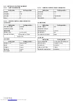


SEMICONDUCTOR SHAPES
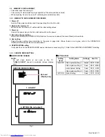
CONTENTS
SEMICONDUCTOR SHAPES ......................................................................2-2
WIRING DIAGRAM ........................................................................................2-3
BLOCK DIAGRAM ........................................................................................2-5
CIRCUIT DIAGRAMS
MAIN PWB CIRCUIT DIAGRAM ................................................................................................................ 2-7
KEY PWB CIRCUIT DIAGRAM ................................................................................................................. 2-17
LED PWB CIRCUIT DIAGRAM ................................................................................................................. 2-18
POWER PWB CIRCUIT DIAGRAM [LT-26AX5, LT-26AX5/S] ................................................................... 2-19
POWER PWB CIRCUIT DIAGRAM [LT-32AX5, LT-32AX5/S] ................................................................... 2-25
PATTERN DIAGRAMS
MAIN PWB PATTERN .............................................................................................................................. 2-31
POWER PWB PATTERN .......................................................................................................................... 2-35
KEY PWB PATTERN ................................................................................................................................ 2-37
LED PWB PATTERN ................................................................................................................................ 2-37
VOLTAGE CHATRS................................................................................... 2-38
WAVEFORMS ............................................................................................ 2-39
USING P.W. BOARD
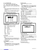
IC
BOTTOM VIEW
FRONT VIEW
TOP VIEW
1
N
N
1
OUT
E
IN
IN
OUT
E
1
N
TOP VIEW
1
N
1
N
CHIP IC
TRANSISTOR
BOTTOM VIEW
FRONT VIEW
TOP VIEW
CHIP TR
E
C
B
E C B
C
B
E
B
(G)
E
(S)
C
(D)
E
C
B
E C B
P.W.B ASS’Y name
MAIN P.W BOARD
POWER P.W BOARD
LED P.W BOARD
KEY P.W BOARD
QAL0791-001
QAL0793-001
QAL0794-001
QAL0795-001
LT-26AX5
LT-26AX5/S
LT-32AX5
LT-32AX5/S
QAL0792-001
2-2(No.YA344)
Summary of Contents for LT-26AX5
Page 37: ... No YA344 2 31 2 32 No YA344 TOP PATTERN DIAGRAMS MAIN PWB PATTERN SOLDER SIDE ...
Page 38: ...2 34 No YA344 No YA344 2 33 TOP MAIN PWB PATTERN PARTS SIDE ...
Page 42: ...2 40 No YA344 ...
Page 44: ...WIDE LCD PANEL TV INSTRUCTIONS LT 32AX5 LT 26AX5 ENGLISH LCT1926 001A H ...
Page 45: ......
Page 85: ...40 ENGLISH ...
Page 86: ......
Page 87: ... 2005 Victor Company of Japan Limited 0805HHH CR JMT ...