background image

1-4 (No.MA345)

KW-XG506/KW-XG505

Design and specifications are subject to change without notice.

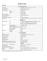
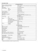
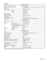
AUDIO AMPLIFIER SECTION

Maximum Power Output

Front and rear

50 W per channel

Continuous Power Output
(RMS)

Front and rear

19 W per channel into 4 

, 40 Hz to 20 000 Hz at no more than 0.8% total har-

monic distortion.

Load Impedance

 (4 

 to 8 

 allowance)

Tone Control Range

Bass

±12 dB at 60 Hz

Mid-range

±12 dB at 1 kHz

Treble

±12 dB at 10 kHz

Frequency Response

40 Hz to 20 000 Hz

Line-Out Level/Impedance

2.5 V/20 k

 load (full scale)

Output Impedance

1 k

Subwoofer-Out Level/Impedance

2.5 V/20 k

 load (full scale)

Other Terminal

CD changer, Subwoofer input, AUX (auxilliary) input jack

TUNER SECTION

Frequency Range

FM

87.5 MHz to 108.0 MHz

AM

531 kHz to 1 602 kHz

FM Tuner

Usable Sensitivity

11.3 dBf (1.0 

µ

V/75 

)

50 dB Quieting Sensitivity

16.3 dBf (1.8 

µ

V/75 

)

Alternate Channel Selectivity (400 kHz) 65 dB

Frequency Response

40 Hz to 15 000 Hz

Stereo Separation

30 dB

AM Tuner

Sensitivity

20 

µ

V

Selectivity

35 dB

CD PLAYER SECTION

Type

Compact disc player

Signal Detection System

Non-contact optical pickup (semiconductor laser)

Number of Channels

2 channels (stereo)

Frequency Response

5 Hz to 20 000 Hz

Dynamic Range

96 dB

Signal-to-Noise Ratio

98 dB

Wow and Flutter

Less than measurable limit

MP3 Decoding Format: (MPEG1/2 Audio Layer 3)

Max. Bit Rate: 320 kbps

WMA (Windows Media® Audio) Decoding Format

Max. Bit Rate: 192 kbps

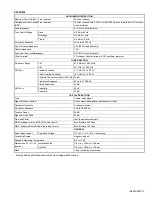
GENERAL

Power Requirement

Operating Voltage

DC 14.4 V (11 V to 16 V allowance)

Grounding System

Negative ground

Allowable Operating Temperature

0

°

C to +40

°

C

Dimensions (W 

×

 H 

×

 D)

(approx.)

Installation Size

178 mm 

×

 100 mm 

×

 158 mm

Set Size

178 mm 

×

 100 mm 

×

 178 mm

Mass

1.8 kg (excluding accessories)

Summary of Contents for KW-XG500J

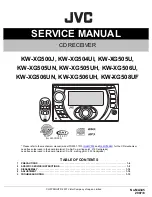
Page 1: ...tor Company of Japan Limited Please refer to the mechanism manual model TN2007 1010 No MY005 and No MY005B for the CD mechanism Lead free solder used in the board material Sn Ag Cu melting point 219 Centigrade Lead free solder used in the board material Sn Cu melting point 230 Centigrade TABLE OF CONTENTS 1 PRECAUTIONS 1 6 2 SPECIFIC SERVICE INSTRUCTIONS 1 9 3 DISASSEMBLY 1 10 4 ADJUSTMENT 1 14 5 ...

Page 2: ... kHz to 1 602 kHz with channel interval set to 9 kHz FM Tuner Usable Sensitivity 11 3 dBf 1 0 µV 75 Ω 50 dB Quieting Sensitivity 16 3 dBf 1 8 µV 75 Ω Alternate Channel Selectivity 400 kHz 65 dB Frequency Response 40 Hz to 15 000 Hz Stereo Separation 35 dB AM Tuner Sensitivity 20 µV Selectivity 35 dB CD PLAYER SECTION Type Compact disc player Signal Detection System Non contact optical pickup semic...

Page 3: ...2 kHz FM Tuner Usable Sensitivity 11 3 dBf 1 0 µV 75 Ω 50 dB Quieting Sensitivity 16 3 dBf 1 8 µV 75 Ω Alternate Channel Selectivity 400 kHz 65 dB Frequency Response 40 Hz to 15 000 Hz Stereo Separation 30 dB AM Tuner Sensitivity 20 µV Selectivity 35 dB CD PLAYER SECTION Type Compact disc player Signal Detection System Non contact optical pickup semiconductor laser Number of Channels 2 channels st...

Page 4: ...1 602 kHz FM Tuner Usable Sensitivity 11 3 dBf 1 0 µV 75 Ω 50 dB Quieting Sensitivity 16 3 dBf 1 8 µV 75 Ω Alternate Channel Selectivity 400 kHz 65 dB Frequency Response 40 Hz to 15 000 Hz Stereo Separation 30 dB AM Tuner Sensitivity 20 µV Selectivity 35 dB CD PLAYER SECTION Type Compact disc player Signal Detection System Non contact optical pickup semiconductor laser Number of Channels 2 channel...

Page 5: ...31 kHz to 1 602 kHz FM Tuner Usable Sensitivity 11 3 dBf 1 0 µV 75 Ω 50 dB Quieting Sensitivity 16 3 dBf 1 8 µV 75 Ω Alternate Channel Selectivity 400 kHz 65 dB Frequency Response 40 Hz to 15 000 Hz Stereo Separation 30 dB AM Tuner Sensitivity 20 µV Selectivity 35 dB CD PLAYER SECTION Type Compact disc player Signal Detection System Non contact optical pickup semiconductor laser Number of Channels...

Page 6: ... formed during molding may be left over on some parts of the chassis Therefore pay attention to such burrs in the case of preforming repair of this system Please use enough caution not to see the beam directly or touch it in case of an adjustment or operation check ...

Page 7: ...ptical pickup The tester s internal power source can easily destroy the laser diode 1 3 Handling the traverse unit optical pickup 1 Do not subject the traverse unit optical pickup to strong shocks as it is a sensitive complex unit 2 Cut off the shorted part of the flexible cable using nippers etc after replacing the optical pickup For specific details refer to the replacement procedure in the text...

Page 8: ... uses visible and or invisible laser radiation and is equipped with safety switches which prevent emission of radiation when the drawer is open and the safety interlocks have failed or are defeated It is dangerous to defeat the safety switches 5 CAUTION If safety switches malfunction the laser is able to function 6 CAUTION Use of controls adjustments or performance of procedures other than those s...

Page 9: ... No MA345 1 9 SECTION 2 SPECIFIC SERVICE INSTRUCTIONS This service manual does not describe SPECIFIC SERVICE INSTRUCTIONS ...

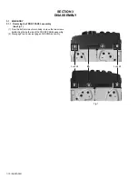
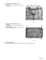
Page 10: ...MAIN BODY 3 1 1 Removing the FRONT PANEL assembly See Fig 1 1 From the bottom side of main body remove the two screws A attaching the both side of the FRONT PANEL assembly 2 Disengage two hooks a engaged CHASSIS assembly Fig 1 A hook a hook a ...

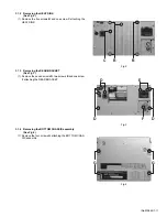
Page 11: ...ching the HEAT SINK Fig 2 3 1 3 Removing the REAR BRACKET See Fig 3 1 Remove the seven screws D two screws E and one screw F attaching the REAR BRACKET Fig 3 3 1 4 Removing the BOTTOM CHASSIS assembly See Fig 4 1 Remove the four screws G attaching the BOTTOM CHAS SIS assembly Fig 4 B B C D D D F E G G ...

Page 12: ...ly 3 Straighten hook b attaching the FUNC BOARD assembly 3 1 6 Removing the MIDDLE CHASSIS See Fig 5 1 Remove the four screws J attaching the MIDDLE CHAS SIS 2 Disconnect the connector CN501 of the main board on the MIDDLE CHASSIS from the CD mechanism assembly in an upward direction Fig 5 3 1 7 Removing the MAIN BOARD assembly See Fig 6 1 Remove the four screws K attaching the MAIN BOARD as sembl...

Page 13: ...g 7 3 1 9 Removing the SWITCH BOARD assembly See Fig 8 1 Remove the volume knob from the front side of the FRONT PANEL assembly 2 Remove the thirteen screws M and two screws N attaching the SWITCH BOARD assembly Fig 8 3 2 CD MECHANISM assembly For CD MECHANISM ASSEMBLY please refer MODEL TN2007 1010 No MY005 and No MY005B L L M M N M ...

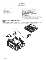
Page 14: ...alance and Bass Treble volume lndication 0 Loudness OFF 4 1 4 Dummy load Exclusive dummy load should be used for AM and FM For FM dummy load there is a loss of 6dB between SSG output and an tenna input The loss of 6dB need not be considered since direct reading of figures are applied in this working standard 4 1 5 How to connect the extension cable for adjusting Caution Be sure to attach the heat ...

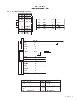
Page 15: ...ONLY GND 16 YL 8 BK 7 RD 15 OR WH 3 GN 11 GN BK 2 VI 10 VI BK 4 WH 12 WH BK 1 GY 9 GY BK 5 BL WH MEMORY GND ACC ILL RL RL RR RR FL FL FR FR REMOTE 13 BR TEL BK RD BL WH BR Black Red Blue White Brown GN VI GY YL OR Green Violet Gray Yellow Orange RR FR FL RL TEL Rear Right Front Right Front Left Rear Left Telephone muting REMOTE ACC MEMORY ILL Remote out ACC Line Memory Backup Battery Ground Illumi...

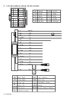
Page 16: ... RD BK Red BL Blue WH White GN Green VI Violet GY Gray OR Orange YL Yellow RR FR FL RL REMOTE ANT ACC ILL GND MEMORY Rear Right Front Right Front Left Rear Left Remote out ACC Line Illuminations Control Ground Memory Backup Battery Auto Antenna BR Brown TEL Telephone muting 16 YL 8 BK 7 RD 15 OR WH 13 BR 3 GN 11 GN BK 2 VI 10 VI BK 4 WH 12 WH BK 1 GY 9 GY BK 5 BL WH 6 BL MEMORY GND ACC ILL TEL RL ...

Page 17: ... RD1 YL1 BK BL GN GN BK VI VI BK WH BK GY GY BK RD3 RD2 YL 2 WH 1 3 5 7 2 4 6 8 NC YL2 OR WH RD2 BK 1 3 5 7 2 4 6 8 VI GY WH GN VI BK GY BK WH BK GN BK BK RD BL WH BR Black Red Blue White Brown GN VI Violet GY Gray YL Yellow YL1 BR NC Green BR BL WH BK BL OR WH BR BL WH 7 8 5 2 4 6 7 1 5 6 3 4 8 2 7 16 8 13 15 6 2 11 3 12 4 10 9 1 5 OR Orange ...

Page 18: ... No MA345 VPT Printed in Japan Victor company of Japan Limited Mobile Entertainment Business Group Mobile Entertainment Category 10 1 1chome Ohwatari machi Maebashi city 371 8543 Japan ...

Page 19: ... model TN2007 1010 No MY005 MY005B for the CD mechanism Contents Exploded view of general assembly and parts list Block No M1 Electrical parts list Block No 01 03 Packing materials and accessories parts list Block No M3 KW XG500J KW XG504UI KW XG505U KW XG505UN KW XG505UH KW XG506U KW XG506UN KW XG506UH KW XG508UF 3 2 3 6 3 12 MA345 ...

Page 20: ... f g j c r h k n Main board F E KW XG500J only D E C d e p p Switch board S M MY005 MY005B model TN2007 1010 G c r C 20 16 10 11 25 36 18 27 15 14 50 15 12 38 29 37 38 1 49 10 5 17 4 35 28 32 24 21 18 33 23 30 34 8 48 43 44 39 6 22 31 26 53 54 55 56 Block No M M M 1 ...

Page 21: ...A b f B g j h k Main board Function board G500J only F D G d m m e c r C 50 15 12 38 37 38 49 8 8 7 13 45 46 47 2 7 51 19 8 9 40 48 41 42 52 9 3 43 44 54 55 M M The parts without symbol number are not service ...

Page 22: ...27 GE32727 002A PRESET BUTTON L 500J 506U 506UN 506UH 508UF 27 GE32727 001A PRESET BUTTON L 504UI 505U 505UN 505UH 28 GE32728 002A PRESET BUTTON R 500J 506U 506UN 506UH 508UF 28 GE32728 001A PRESET BUTTON R 504UI 505U 505UN 505UH 29 GE32730 002A SEL EQ BUTTON 500J 29 GE32730 001A SEL EQ BUTTON 504UI 505U 505UN 505UH 506U 506UN 506UH 508UF 30 GE20223 001A VOLKNOB COVER 500J 30 GE20223 002A VOLKNOB ...

Page 23: ...3 5 53 GE40218 078A SHEET 54 QYSDST2606ZA TAP SCREW M2 6 x 6mm 500J 55 QAM0991 001 STEELING REMOTE 500J 56 GE40402 001A TOP SHEET 508UF Symbol No Part No Part Name Description Local ...

Page 24: ...J D720 1SS355W X DIODE D720 or MA111 X SI DIODE D781 1SS355W X DIODE D781 or MA111 X SI DIODE D782 1SS355W X DIODE D782 or MA111 X SI DIODE D783 1SS355W X DIODE D783 or MA111 X SI DIODE D784 UDZW9 1B X Z DIODE D784 or MA8091 M X Z DIODE D851 MA22D23 X SB DIODE 504UI 505 U 505UN 505UH 50 6U 506UN 506UH 50 8UF D851 or CRS03 W SB DIODE 504UI 505 U 505UN 505UH 50 6U 506UN 506UH 50 8UF D851 or RB160M 3...

Page 25: ...OR 0 1uF 25V K C559 QEKJ1CM 476Z E CAPACITOR 47uF 16V M C560 NCB31EK 104X C CAPACITOR 0 1uF 25V K C561 NCB31EK 104X C CAPACITOR 0 1uF 25V K Symbol No Part No Part Name Description Local C562 QEKJ1CM 476Z E CAPACITOR 47uF 16V M C563 NCB31EK 104X C CAPACITOR 0 1uF 25V K C564 NDC31HJ 680X C CAPACITOR 68pF 50V J C565 NCB31EK 153X C CAPACITOR 0 015uF 25V K C566 NCB31EK 104X C CAPACITOR 0 1uF 25V K C567...

Page 26: ...3kΩ 1 16W J R519 NRSA63J 123X MG RESISTOR 12kΩ 1 16W J R520 NRSA63J 822X MG RESISTOR 8 2kΩ 1 16W J R521 NRSA63J 152X MG RESISTOR 1 5kΩ 1 16W J R522 NRSA63J 152X MG RESISTOR 1 5kΩ 1 16W J R523 NRSA63J 152X MG RESISTOR 1 5kΩ 1 16W J R524 NRSA63J 151X MG RESISTOR 150Ω 1 16W J R525 NRS181J 101X MG RESISTOR 100Ω 1 8W J R526 NRS181J 101X MG RESISTOR 100Ω 1 8W J R527 NRSA63J 473X MG RESISTOR 47kΩ 1 16W J...

Page 27: ...63J 0R0X MG RESISTOR 0Ω 1 16W J R790 NRSA63J 101X MG RESISTOR 100Ω 1 16W J R797 NRSA63J 103X MG RESISTOR 10kΩ 1 16W J R801 NRSA63J 473X MG RESISTOR 47kΩ 1 16W J R802 NRSA63J 473X MG RESISTOR 47kΩ 1 16W J R803 NRSA63J 101X MG RESISTOR 100Ω 1 16W J R804 NRSA63J 223X MG RESISTOR 22kΩ 1 16W J R805 NRSA63J 104X MG RESISTOR 100kΩ 1 16W J R806 NRSA63J 103X MG RESISTOR 10kΩ 1 16W J R807 NRSA63J 104X MG RE...

Page 28: ...ISTOR 47kΩ 1 16W J R6203 NRSA63J 471X MG RESISTOR 470Ω 1 16W J R6204 NRSA63J 0R0X MG RESISTOR 0Ω 1 16W J R6206 NRSA63J 103X MG RESISTOR 10kΩ 1 16W J R6207 NRSA63J 471X MG RESISTOR 470Ω 1 16W J Symbol No Part No Part Name Description Local R6300 NRSA63J 821X MG RESISTOR 820Ω 1 16W J R6301 NRSA63J 102X MG RESISTOR 1kΩ 1 16W J R6302 NRSA63J 122X MG RESISTOR 1 2kΩ 1 16W J R6303 NRSA63J 182X MG RESISTO...

Page 29: ...16W J R331 NRSA63J 821X MG RESISTOR 820Ω 1 16W J R332 NRSA63J 181X MG RESISTOR 180Ω 1 16W J R335 NRSA63J 0R0X MG RESISTOR 0Ω 1 16W J CN322 QGA2001F1 07 CONNECTOR W B 1 7 J321 QNN0294 001 PIN JACK Symbol No Part No Part Name Description Local ...

Page 30: ...cessories parts list Block No M M M 3 KIT P1 P2 P4 P6 P5 P7 P3 The parts without symbol number are not service A10 A12 A11 A7 A1 A2 A3 A4 A5 A6 A13 A14 A15 A16 A8 A9 No additional supplemental order of WARRANTY CARDs are available ...

Page 31: ... MANUAL RUS 505U 506U A 7 GE20224 002A TRIM PLATE 504UI 505U 505UN 505UH A 7 GE20224 001A TRIM PLATE 506U 506UN 506UH 508UF A 8 QYSDSP5008ZA SCREW M5 x 8mm x8 A 9 QYSSSP5008ZA SCREW M5 x 8mm x8 A 10 QAM0675 001 CAR CABLE 500J A 10 QAM0308 004 POWER CORD 504UI 505U 505UN 505UH 506U 506UN 506UH A 10 QAM0980 001 POWER CORD 508UF A 11 RM RK50C REMOCON A 12 BATTERY 3V A 13 WARRANTY CARD BT 51018 5 500J...

Page 32: ... XG505U KW XG505UN KW XG505UH KW XG506U KW XG506UN KW XG506UH KW XG508UF COPYRIGHT 2007 Victor Company of Japan Limited Lead free solder used in the board material Sn Ag Cu melting point 219 Centigrade Lead free solder used in the board material Sn Cu melting point 230 Centigrade for KW XG500 Please refer to the mechanism manual model TN2007 1010 No MY005 MY005B for the CD mechanism ...

Page 33: ...r on some parts of the chassis Therefore pay attention to such burrs in the case of preforming repair of this system Safety precaution Please use enough caution not to see the beam directly or touch it in case of an adjustment or operation check ...

Page 34: ...V CD8V 9V ILMI ACC EXT MEMORY ANTCONT ILLUMINATION Used for except KW XG500 Used for KW XG500 IC801 JVC BUS SO I O SI SO INT SCK SI SO BUSCK J801 JVC BUS CN261 J321 CD servo control section Front panel section TELMUTE TELMUTE Q976 Q977 PS2 PS2 Q881 DIMMER INPUT DIMIN POWER X702 32 768kHz D6101 to D6127 Q6001 Q6002 LIGHTING DISPLAY BCK LRCK DATA MUTING MUTE SCK X701 20MHz Q261 Q262 SUBWOOFER MUTING...

Page 35: ...X 820 820 0 047 820 820 100 180 180 180 180 0 0 1SS355W X 47k 1 2k 1k 0 10k 2 2k 2 2k 4 7 25 0 047 10k 0 0047 47 16 1 50 0 1 50 100 0 0047 NFV81CM 105X 0 0047 0 0047 0 0047 4 7 16 47K 100 47k QAX0401 001 100 16 0 1 0 0047 0 0047 0 0047 QAX0916 001Z 0 1 RT6N430C X RT6N430C X RT6N430C X 12k 27k 1SS355W X QNZ0611 001 2SA1530A QR X NFV81CM 105X UDZW6 2B X 4 7k 4 7k 4 7k 2 2 50 0 082 0 01 1K 1K 1K 1K 1...

Page 36: ... 5k 6 8k 8 2k 10K 7 5k 0 1 270P 0 027 0 018 220 100 47u 0 1 22 16 47 16 22p 22p 22p SN74CBT3245AP X 0 1 0 1 0 0 01 0 22p 1 2K 150 100p 10 100 100 47K 10k 10k 100 0 0 0 022 8 2k 27k 1 5k 1 5k 0 01 0 001 100 100 100 10k 10k 10k 100 12p 0 1 15p NAX0375 001X 27k 8 2k 150p 0 1 150p 1A3G T1 22k 47 16 1K TC74VHCU04FT X 0 01 22k 0 1 100 100 4 7 25 4 7 25 47k 24k 24k 820p 100k 820p 47 16 RT1N141C X 0 01 47...

Page 37: ...S BRST 680 680 RT1N141C X 1 2K 1 2K NSW0246 001X NSW0206 001X NSW0206 001X NSW0206 001X NSW0206 001X NSW0206 001X NSW0206 001X NSW0206 001X NSW0206 001X NSW0206 001X NSW0206 001X 430 1K 4 7K 820 LHQ974 LM X LHQ974 LM X 430 NSPW310BS BRST 680 680 LHQ974 LM X LHQ974 LM X LHQ974 LM X LHQ974 LM X LHQ974 LM X LHQ974 LM X LHQ974 LM X LHQ974 LM X LHQ974 LM X LHQ974 LM X LHQ974 LM X LHQ974 LM X LHQ974 LM ...

Page 38: ...581 R583 R584 R585 R586 R589 R591 R593 R595 R596 R599 R601 R602 R603 R604 R605 R606 R607 R608 R609 R611 R612 R615 R616 R617 R618 R619 R621 R625 R626 R635 R639 R641 R643 R644 R647 R651 R661 R662 R663 R664 R665 R666 R667 R668 R671 R672 R673 R674 R675 R676 R677 R678 R682 R683 R684 R685 R686 R688 R689 R690 R691 R692 R694 R702 R704 R705 R706 R709 R710 R712 R713 R714 R715 R716 R717 R718 R719 R720 R721 R...

Page 39: ...63 09 S6310 S6311 S63 12 S63 13 S6314 S6315 S6316 S6317 C6001 C6201 C6202 C6203 C6204 C6301 C6302 C6401 C6402 C6403 C6411 C6412 C6413 CN601 CN602 CN603 D6101 D6102 D6103 D6130 D6201 D6202 D6360 D6361 D6401 D6402 D6411 D6412 EN601 IC604 IC602 IC603 K6360 L6360 PJ601 Q6001 Q6002 R6001 R6002 R6003 R6101 R6102 R6103 R6104 R6105 R6106 R6107 R6108 R6109 R6110 R6111 R6112 R6113 R6114 R6117 R6118 R6119 R6...

Page 40: ... M E M O ...
Page 41: ... No MA345SCH Printed in Japan VPT Mobile Entertainment Business Group Mobile Entertainment Category 10 1 1chome Ohwatari machi Maebashi city Gumma ken 371 8543 Japan Victor Company of Japan Limited ...

Reviews: