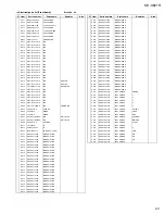
JVC KD-S821R Service Manual Download Page 50

H

A

B

C

D

E

F

G

1

2

3

4

5

KD-S821R

KD-S821R

2-6

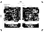
Printed circuit boards

Main board

Front board

(Forward side)

(Forward side)

Front board

(Reverse side)

Main board

(Reverse side)

C3

C5

C9

C10

C31

C42

C43

C51

C52

C53

C54

C55

C74

C76

C161

C164

C165

C167

C168

C169

C171

C181

C184

C187

C188

C189

C191

C242

C243

C244

C321

C322

C331

C332

C341

C342

C351

C352

C501

C503

C523

C524

C525

C526

C527

C530

C541

C543

C544

C545

C546

C547

C548

C549

C550

C551

C552

C553

C555

C556

C557

C558

C559

C560

C563

C569

C571

C572

C581

C582

C583

C584

C591

C592

C593

C594

C595

C703

C704

C706

C708

C781

C782

C802

C891

C901

C903

C904

C905

C907

C908

C911

C912

C913

C914

CN501

CP601

CP961

D1

D2

D241

D242

D162

D161

D501

D891

D782

D182

C309

C310

R310

R782

D910

IC71

IC161

IC501

IC521

IC541

IC581

D911

J1

J301

J801

L1

L541

L542

L701

Q2

Q3

Q5

Q51

Q52

Q32

Q161

Q162

Q181

Q241

Q321

Q331

Q341

Q351

Q501

Q521

Q781

Q782

Q783

Q891

Q976

Q977

R4

R5

R8

R32

R33

R43

R51

R53

R55

R57

R168

R169

R170

R188

R244

R245

R323

R333

R343

R353

R502

R503

R504

R526

R527

R528

R530

R534

R541

R542

R543

R544

R545

R546

R547

R548
R549

R550

R551

R552

R553

R554

R555

R581

R584

R585

R586

R591

R594
R595

R596

R703

R704

R705

R706

R709

R710

R711

R712

R713

R714

R716

R717

R718

R723

R725

R730

R731

R738

R739

R742

R743

R810

R781

R802

R803

R804

R805

R806

R807

R808

R809

R891

R892

R901

R902

R907

R977

R978

TU1

X71

X541

X701

L961

C302

C303 C304

C301

C305

C306

C307

C308

IC701

B731

R745

R744

R746

R747

D41

D502

C915

C783

B733

R508

R507

B501

R708

R707

C760

IC301

C316

C317

C391

C392

C393

C394

D991

D992

D993

D994

D995

D996

D997

D998

IC961

R904

C770

B706

S701

J302

D781

D892

D351

D341

D321

D331

B52

.

.

.

.

.

.

.

.

.

.

.

.

.

.

.

.

.

.

.

.

.

.

.

.

.

.

.

.

.

.

.

.

1

30

50

51

80

81

100

1

12

13

24

1

14

15

28

1

30

31

50

51

80

81

100

1

16

17

32

GEB10007A

31

S1B

B51

C1

C2

C3

C4

C5

C6

C7

C8

C9

C31

C32

C41

C43

C51

C71

C72

C73

C74

C75

C76

C77

C161

C162

C163

C164

C166

C167

C168

C169

C171

C172

C173

C181

C182

C183

C184

C185

C186

C187

C188

C189

C191

C192

C243

C244

C311

C312

C321

C331

C341

C351

C501

C502

C503

C521

C522

C524

C526

C527

C528

C529

C530

C531

C532

C533

C541

C542

C543

C544

C546

C549

C553

C554

C558

C561

C562

C563

C564

C565

C566

C567

C568

C569

C570

C571

C572

C573

C582

C583

C592

C593

C595

C701

C702

C706

C707

C708

C718

C781

C782

C801

C901

C902

C903

C904

C905

C907

C908

C909

C911

C912

C913

C914

C313

CN501

CP601

CP961

D1

D2

D707

D784

D241

D242

D501

D782

C315

C309

C310

B314

D912

D4

D911

IC801

B732

J1

J301

J801

L1

L541

L542

L701

B310

Q1

Q4

Q31

Q41

Q42

Q501

Q521

Q751

R1

R2

R3

R6

R7

R9

R10

R31

R41

R42

R44

R52

R54

R56

R71

R72

R73

R161

R162

R163

R164

R165

R166

R167

R181

R182

R183

R184

R185

R186

R187

R241

R242

R243

R246

R247

R321

R322

R324

R331

R332

R334

R341

R342

R344

R351

R352

R354

R501

R521

R522

R523

R524

R525

R529

R531

R532

R533

R556

R557

R558

R582

R583

R592

R593

R701

R702

R715

R719

R720

R721

R722

R724

R726
R727

R728
R729

R732

R733

R734

R736

R737

R740

R750

R751

R801

R686

R685

R905

R906

R907

R911

TP1

TP2

TU1

X71

X541

X701

L961

B305

B306

B307

B308

B309

B303

B302

B313

B315

B316

C713

D901

X1

SO

VSS

VDD

SCK

SI

RESET

VPP

LM0

LM1

D3

Q7

Q174

C720

C719

B174

C714

D502

C915

C933

C721

Q53

R58

C776

B318

B317

R506

Q43

C44

IC301

C316

C317

IC961

B904

B901

S701

R753

J302

B324

D701

D702

D703

D704

D705

D706

B903

D709

D708

D710

D711

C241

ACC

REM

GND

MEM

GND

FM/AMOSC
FMVCC

AMVCC

GND

AMVT

MUTE

FMANT

AMANT

R-CH

SNC

SD/ST

NC

NC

FMVT

25

26

DET.

ENC.2

10V

5V

2

RF

ACC.IN

GND

NC

VCC

NC

REMOTE

SW5V

MEM.DET

1

GND

VREF

23

TEL-MUTE

ANTCTRL

NC

NC

ENC.1

REMO

DATA

COMP.OUT

S.METER

SEEK/STOP

VCC

L-CH

1

CTRL

AJ

GND

ILM.10V

CD.8V

A.9V

MEM.IN

ACC.5V

VDD.5V

SCK

CE

KEY0

KEY2

KEY1

T1B

D601

D602

D603

D604

D605

D606

D607

D608

D609

D610

D611

D613

D614

D615

D616

D617

D618

D619

D620

D621

D622

D623

D624

D625

D644

IC602

JS690

LCD1

R601

R602

R603

R604

R605

R608

R609

R610

R616

R632

R633

R634

R635

R638

R639

R644

R645

R655

S601

S602

S603

S604

S605

S606

S607

S608

S609

S610

S611

S612

S613

S614

S615

S616

S617

S618

S619

D645

GEB10018A

S1B

C601

C602

C603

C611

C681

C682

CJ601

D644

IC602

R606

R607

R611

R612

R613

R614

R615

R631

R636

R637

R640

R641

R642
R643

R646

R647

R651

R652

R653

R654

R656

R657

R658

R661

R662

R681

D645

R659

R649

R648

C612

D642

D643

D641

R660

D646

15

1

1

T1C

Summary of Contents for KD-S821R

Page 1: ...on Preventing static electricity Disassembly method Adjustment method 1 2 1 3 1 4 1 11 Flow of functional operation unit TOC read Maintenance of laser pickup Replacement of laser pickup Description of major ICs 2 1 2 3 2 3 2 6 E Continental Europe EX Central Europe 45Wx4 KD S821R 7 8 9 10 11 12 RDS MO RND DISP TP PTY SCM COMPACT DIGITAL AUDIO ...

Page 2: ...ft over on some parts of the chassis Therefore pay attention to such burrs in the case of preforming repair of this system Safety precaution Please use enough caution not to see the beam directly or touch it in case of an adjustment or operation check ...

Page 3: ...cement return the shorted parts to their original condition Refer to the text 2 Do not use a tester to check the condition of the laser diode in the optical pickup The tester s internal power source can easily destroy the laser diode 4 Handling the traverse unit optical pickup 1 Do not subject the traverse unit optical pickup to strong shocks as it is a sensitive complex unit 2 Cut off the shorted...

Page 4: ... following procedure remove the front panel assembly Release the four joint tabs a on both sides of the front chassis assembly and remove the front chassis assembly toward the front 1 Removing the front chassis assembly See Fig 2 and 3 Disassembly method Main body Fig 1 Fig 2 Fig 3 Front panel assembly Eject button Tab a Tab a Front chassis assembly Front chassis assembly Heat sink Tab a Tab a ...

Page 5: ...ve the front panel assembly the front chassis assembly and the heat sink Turn over the body and unjoint the five joints b with the bottom cover and the body using a screwdriver 1 Removing the bottom cover See Fig 5 and 6 Fig 4 Fig 5 Fig 6 Heat sink A Joints b Joints b Joint b Joints b Joints b Joint b Bottom cover Bottom cover Rear panel Rear panel A ...

Page 6: ...n the bottom of the body Disconnect connector CN501 on the main board in the direction of the arrow 1 2 Removing the main board See Fig 7 and 8 Prior to performing the following procedure remove the front panel assembly the front chassis assembly the heat sink the bottom cover and the main board Remove the three screws F attaching the CD mechanism section on the back of the top chassis 1 Removing ...

Page 7: ...ck of the front panel assembly Unjoint the twelve joints c with the front panel and the rear cover Remove the control switch board on the back of the front panel 1 2 3 Removing the control switch board See Fig 10 to 12 Fig 10 Fig 11 Fig 12 G G G G Rear cover Front panel Control switch board Joints c Joints c Front panel Rear cover Joints c Joints c ...

Page 8: ...ickup unit to the appropriate position where the flexible wire of the CD mechanism unit can be disconnected easily Refer to Fig 2 ATTENTION Prior to performing the following procedure remove the CD mechanism control board Remove the two springs f attaching the CD mechanism assembly and the front bracket Remove the two screws B and the front bracket while pulling the flame outward Remove the belt a...

Page 9: ... two screws E and both sides rear damper brackets from the dampers Detach the CD mechanism assembly from the left side to the right side 1 2 3 4 Removing the CD mechanism assembly See Fig 1 6 to 9 The CD mechanism assembly can be removed if only the rear damper bracket on the left side is removed ATTENTION Fig 6 Fig 7 Fig 8 Fig 9 Rear damper bracket Fix arm R Damper D D Damper bracket CD mechanism...

Page 10: ...kup mount nut from the pickup unit Pull out the FD screw 2 Removing the pickup unit See Fig 10 and 11 When reattaching the pickup unit reattach the part j of the pickup unit then the part i of the FD screw ATTENTION Prior to performing the following procedure remove the CD mechanism control board the front bracket loading motor the CD mechanism assembly and the feed motor assembly Turn up the CD m...

Page 11: ... allowance Load impedance 4 4 to 8 allowance Line Out Level Impedance 2 0V 20k load full scall Output Impedance 1k How to connect the extension cable for adjusting Dummy load Exclusive dummy load should be used for AM and FM For FM dummy load there is a loss of 6dB between SSG output and antenna input The loss of 6dB need not be considered since direct reading of figures are applied in this workin...

Page 12: ... ON When the laser diode correctly emits Microprocessor commands Rough Servo Mode CLV Servo Mode ProgramArea CLV Servo Mode Lead In Area Digital 0 RF signal Flow of functional operation until TOC read When the pickup correctly moves to the inner area of the disc TERMINAL Microprocessor commands FMO TC9462 53 FEED MOTOR TERMINAL IC501 10 REST SW When the disc correctly rotates Tracking Servo Loop O...

Page 13: ...s 14 18 Check the pickup and its connections NO YES YES YES Does the S search waveform appear at IC501 pins 6 and 7 Is the disk rotated Does the RF signal appear at TP1 Is 4V present at IC501 pins 8 and 9 Check the spindle motor and its wiring Is 4V present at IC541 pin 55 Check the vicinity of IC501 Check IC521 and IC541 YES NO NO NO NO NO YES YES YES Check the circuits in the vicinity of IC521 2...

Page 14: ...ce this adjustment should be performed to match the characteristics of the whole optical block do not touch the semi fixed resistor If the laser power is lower than the specified value the laser diode is almost worn out and the laser pickup should be replaced If the semi fixed resistor is adjusted while the pickup is functioning normally the laser pickup may be damaged due to excessive current Tur...

Page 15: ... and H level to ANT CTRL Connected to ACC Regular 5 7V Output voltage is 5V when M or H level applied to CTRL pin Output for ACC detector L ANT output OFF H ANT output ON Connected to VCC Low battery detect Output voltage is 9V When M or H level applie to CTRL pin L BIAS OFF M BIAS ON H CD ON Output voltage is 8V when H level applied to CTRL pin Adjustment pin for ILM output voltage Output voltage...

Page 16: ...ation line JVC bus communication line JVC bus communication line JVC bus communication line No use Serial data input Serial data output Serial clock output No use LCD driver serial data output Serial data for LCD JVC bus output select No use LCD driver communication line CD mech switch CD mech switch CD mech switch Traverse mech rest switch Encoder input Encoder input Key input Key input Key input...

Page 17: ...output for AM PLL error output for FM Setting to write for flash System reset CD mech switch Remocon input No use No use Power control CD power control Mute control No use No use No use No use CD mech driver control CD mech driver control CD LSI communication line CD LSI communication line CD LSI communication line CD LSI communication line CD LSI communication line CD LSI communication line CD LS...

Page 18: ...UT 2 PWR GND2 R F IN 3 IN 4 PRE GND ON TIME C Muting ON Time Control Circuit Protective circuit Protective circuit Mute circuit Ripple Filter Stand by Switch N C 0 22 F 2200 F 0 022 F 0 22 F TAB 5V ST ON 47 F 0 22 F 0 22 F 22 F Mute 10K 3 3 F OUT 3 OUT 3 Low Level Mute ON PWR GND3 OUT 4 OUT 4 PWR GND4 LA4743K IC301 Power amp 1 Block diagram ...

Page 19: ...19 20 21 22 23 24 25 Symbol Pin No Function Header of IC Power GND Outpur for front Rch Stand by input Output for front Rch Power input Output for rear Rch Power GND Output for rear Rch Ripple filter Rear Rch input Front Rch input Signal GND Front Lch input Rear Lch input Power on time control Output for rear Lch Power GND Output for rear Lch Power input Output for front Muting control input Outpu...

Page 20: ...27 26 25 24 23 22 21 20 19 18 17 16 15 FR 1 2 3 4 5 6 7 8 9 10 11 12 13 14 FR CH 3 4 5 Power supply Output control CH5 CH4 CH2 CH1 CH3 22K 11K 5VREG PNPTr The outside putting 22K 22K 22K 11K 11K 11K CH1 2 Power supply LA6567H X IC501 BTL driver 1 Pin layout blockdiagram Level shift Level shift Level shift Level shift Thermal shutdown Input Signal system power supply ...

Page 21: ...stment Regulator terminal Outside putting PNP base Regulator terminal Outside putting PNP collector Standard voltage input terminal Signal system power supply It is short with VCC1 VCC2 CH4 Input terminal For gain adjustment CH4 Input terminal 5CH VLO Output voltage set terminal Signal system GND 5CH VLO Signal output switch terminal FWD Input of logic of loading part 5CH VLO Signal output switch ...

Page 22: ... equalizer Automatic adjustment circuit ROM RAM CLV servo Address circuit Micon interface Correction circuit Audio out circuit 16KRAM Digital out Sub code decoder Status Synchronous guarantee EFM decode PLL TMAX VCO Data slicer TC9462F IC541 DSP DAC 1 Pin layout Block Diagram PIN No 1 2 3 SYMBOL TEST0 HSO UHSO I O FUNCTIONAL DESCRIPTION Non connected REMARKS With pull up resistor Digital GND termi...

Page 23: ...ut Analog input Analog input Zin 10k Analog output 2VREF AVSS 3 state PWM signal output 2VREF VREF VSS PWM carrier 88 2kHz 3 state output 2VREF VREF VSS 40 41 42 43 44 45 46 47 48 49 50 51 52 53 54 55 56 57 58 61 62 63 64 67 68 69 70 RFCT RFZI RFRP FEI SBAD TSIN TEI TEZI FOO TRO VREF RFGC TEBC FMO FVO DMO 2VREF SEL FLGA D VDD VSS IO0 3 DMOUT CKSE DACT RFRP signal center level input terminal RFRP z...

Page 24: ...ut terminal for system clock Oscillator power supply voltage terminal for system clock Analog GND terminal for DA converter Rch R channel data forward output terminal Analog supply voltage terminal for DA converter Reference voltage terminal for DA converter L channel data forward output terminal Analog GND terminal for DA converter Lch Non connected Micon interface data input output terminal Digi...

Page 25: ...GND CIN SCOUT 1 2 3 4 5 6 7 8 16 15 14 13 12 11 10 9 CLK T57 OSCO OSCI vdd GND TEST MODE Symbol QUAL DATA Vref MUX vdd GND CIN SCOUT MODE TEST GND vdd OSCI OSCO T57 CLK Pin No 1 2 3 4 5 6 7 8 9 10 11 12 13 14 15 16 Description Quality indication output RDS data output Reference voltage output 0 5VDDA Multiplex signal input 5V supply voltage for analog part Ground for analog part 0V Sub carrier inp...

Page 26: ...ohm 20k ohm 20k ohm 13k ohm 680 ohm 2 12k ohm BOTTOM PEAK 20k ohm 20k ohm 20k ohm 12k ohm 1 74k ohm 47k ohm 12k ohm 180k ohm 50uA 21k ohm 21k ohm 7 96k ohm 10k ohm 10k ohm 10k ohm 10k ohm 10pF 36pF 50k ohm 15k ohm 30k ohm 7 67k ohm 10k ohm 30k ohm 15k ohm 20uA 21k ohm 29k ohm 24k ohm 24k ohm 65uA 20pF 180k ohm 20pF 180k ohm 180k ohm 40pF 40pF I I I I SW3 SW2 SW1 1k ohm LDC 3 STATE DET 20pF TEO TEN...

Page 27: ...Sample as Load Circuit 1 Sample as Load Circuit 1 Sample as Load Circuit 1 1k 1k S1 CL Input Output C L H H A X L H Y Z H L 1 2 3 4 5 6 7 14 13 12 11 10 9 8 HD74HC126FP X IC771 Buffer 1 Terminal layout 2 Block diagram 3 Pin function 1C 1A 1Y 2C 2A 2Y GND 3Y 3A 3C 4Y 4A 4C Vcc Note H High L Low X H and L Z H L X ...

Page 28: ... COM3 COM2 COM1 S50 S49 LC75823W IC601 LCD driver 1 Pin Layout Symbol 2 Pin Function Pin No 1 to 50 51 to 52 53 to 55 56 to 60 61 62 63 64 I O O O I O I Segment output pins used to display data transferred by serial data input Non connected Common driver output pins The frame frequency is given by t0 fosc 384 Hz Non connected Oscillator connection An oscillator circuit is formed by connecting an e...

Page 29: ...L IMO INTUL INCDL Serial data input output Ground output left rear output left front Treble control capacitor left channel or input from an external equalizer Bass control capacitor left channel or output to an external equalizer Bass control capacitor left channel Input volume 1 left control part Input loudness left control part Output source selector left channel Not used Not used Input C left s...

Page 30: ... SV4 IC602 Remote sensor Vcc Vcc Comp AGC AMP PD Detector BPF fo trimming circuit I V conversion magnetic shield Rout GND 22k 8 7 6 5 4 3 2 1 V B OUTPUT B INPUT B INPUT A INPUT A INPUT A OUTPUT V NJM4565M WE IC581 CD L P F ...

Page 31: ...KD S821R VICTOR COMPANY OF JAPAN LIMITED MOBILE ELECTRONICS DIVISION PERSONAL MOBILE NETWORK BUSINESS UNIT 10 1 1Chome Ohwatari machi Maebashi city 371 8543 Japan No 49679 200202 ...

Page 32: ... parts Contents Exploded view of general assembly and parts list Block No M1 CD mechanism assembly and parts list Block No MB Electrical parts list Block No 01 02 Packing materials and accessories parts list Block No M3 M5 KD S821R 3 2 3 4 3 7 3 12 Area suffix E Continental Europe EX Central Europe ...

Page 33: ...ral assembly and parts list Block No M M M 1 Front board Main board 24 2 6 1 6 6 28 26 27 25 20 23 17 18 31 32 29 22 21 30 33 19 13 16 12 11 15 14 35 35 34 40 37 39 41 36 38 5 42 4 55 54 56 7 3 8 47 43 46 9 44 48 9 7 10 8 50 51 8 49 45 ...

Page 34: ... BUTTON 1 FM CD AM 23 GE30112 001A PUSH BUTTON 1 24 GE40102 001A REMOTE LENS 1 25 GE30366 001A SEL BUTTON 1 26 FSYH4036 032 SHEET 1 FOR SEL BUTTON 27 GE30546 001A KNOB 1 28 GE30104 001A RIM LENS 1 29 GE20109 001C UP DOWN BUTTON 1 30 GE30106 003A SND FUNC BUTTON 1 31 FSXP3055 001 DETACH BUTTON 1 32 FSKW3002 012 COMP SPRING 1 FOR DETACH BUTTON 33 GE30117 001A LIGHT LENS 1 34 GE10004 001B REAR COVER ...

Page 35: ...3 7 6 19 18 105 48 43 50 41 42 103 49 49 56 107 131 36 107 107 38 32 33 130 106 29 108 106 135 104 107 40 63 39 51 52 109 132 86 113 113 134 80 117 92 84 79 88 93 22 22 89 62 81 82 116 102 101 108 100 133 57 d d c a d a b c b TN CCD1001Z 136J CD mechanism assembly and parts list Block No M M M B Grease G 31SA G 31SA Bottom side RX 405 ...

Page 36: ...30310149T REAR DAM BKT Z 1 22 30310151T HUNG UP SP FZ 2 23 30310129T HUNG UP SP R 2 29 30300510T PU GEAR B 1 32 30310544T F M BASE Z 1 33 30310547T FD GR BLK Z 1 36 30310546T PU GUIDE Z 1 38 30310533T THRUST SPR M 1 39 30310548T PU M NUT Z 1 40 30310512T NUT PUSH SPR PL 1 41 30310558T CLP ARM Z 1 42 30310514T CLP ARM SPRING 1 43 30310552T CLAMPER Z 1 48 30310557T CLAMPER PLATE Z 1 49 30310524T DAM...

Page 37: ...1 9C2020401T C SCREW TS G 5 M2X4 102 9C4320403T C B TAP SCREW 4 M2X4 103 9C0117223T SCREW 2 M1 7X2 2 104 9C0917703T C TAP SCREW S3 1 M1 7X7 105 9C0320201T C TAP SCREW S3 1 M2X2 106 9C4920013T C TAP SCREW S3 2 M2X10 107 9C4920603T C TAP SCREW B3 4 M2X6 108 9P0220031T TAMS SCREW 2 M2X3 109 9C0314203T C TAP SCREW 1 M1 4X2 110 9C0420253 C TAP SCREW 1 M2X2 5 113 9W0330276 NW BLUE 2 2 9X5X0 3 116 9W0725...

Page 38: ... 223X C CAPACITOR C 316 QERF1CM 226Z E CAPACITOR 22MF 20 16V C 317 QERF1CM 476Z E CAPACITOR 47MF 20 16V C 321 QERF1HM 225Z E CAPACITOR 2 2MF 20 50V C 322 NCS31HJ 391X C CAPACITOR C 331 QERF1HM 225Z E CAPACITOR 2 2MF 20 50V C 332 NCS31HJ 391X C CAPACITOR C 341 QERF1HM 225Z E CAPACITOR 2 2MF 20 50V C 342 NCS31HJ 391X C CAPACITOR C 351 QERF1HM 225Z E CAPACITOR 2 2MF 20 50V C 352 NCS31HJ 391X C CAPACI...

Page 39: ...351 1SS355 X DIODE D 501 DSK10C T1 DIODE D 701 UDZS5 6B X Z DIODE D 702 UDZS5 6B X Z DIODE D 703 UDZS5 6B X Z DIODE D 704 UDZS5 6B X Z DIODE D 705 UDZS5 6B X Z DIODE D 706 UDZS5 6B X Z DIODE D 707 UDZS5 6B X Z DIODE D 781 1SS355 X DIODE D 782 1SS133 T1 SI DIODE D 784 UDZ11B X Z DIODE D 891 1SS355 X DIODE D 892 1SS355 X DIODE D 901 1SS355 X DIODE D 910 CRS03 W SB DIODE D 911 1N5401 TU 15 DIODE D 91...

Page 40: ... MG RESISTOR R 354 NRSA63J 101X MG RESISTOR R 501 NRSA63J 822X MG RESISTOR R 502 NRSA63J 562X MG RESISTOR R 503 NRSA63J 242X MG RESISTOR R 504 NRSA63J 203X MG RESISTOR R 506 NRS181J 0R0X MG RESISTOR R 507 NRS181J 822X MG RESISTOR R 508 NRS181J 203X MG REGISTOR R 521 NRSA63J 473X MG RESISTOR R 522 NRSA63J 473X MG RESISTOR R 523 NRSA63J 473X MG RESISTOR R 524 NRSA63J 473X MG RESISTOR R 525 NRSA63J 1...

Page 41: ...SISTOR R 734 NRSA63J 103X MG RESISTOR R 736 NRSA63J 103X MG RESISTOR R 737 NRSA63J 473X MG RESISTOR R 738 NRSA63J 103X MG RESISTOR R 739 NRSA63J 473X MG RESISTOR R 740 NRSA63J 103X MG RESISTOR R 743 NRSA63J 473X MG RESISTOR R 744 NRSA63J 222X MG RESISTOR R 745 NRSA63J 222X MG RESISTOR R 781 NRS181J 273X MG RESISTOR R 782 NRS181J 102X MG RESISTOR R 801 NRSA63J 104X MG RESISTOR R 802 NRSA63J 104X MG...

Page 42: ...SISTOR R 615 NRSA63J 182X MG RESISTOR R 616 NRSA63J 272X MG RESISTOR R 631 NRSA63J 821X MG RESISTOR R 632 NRSA63J 182X MG RESISTOR R 633 NRSA63J 182X MG RESISTOR R 634 NRSA63J 182X MG RESISTOR R 635 NRSA63J 182X MG RESISTOR R 636 NRSA63J 182X MG RESISTOR R 637 NRSA63J 182X MG RESISTOR R 638 NRSA63J 511X MG RESISTOR R 639 NRSA63J 511X MG RESISTOR R 640 NRSA63J 511X MG RESISTOR R 641 NRSA63J 511X MG...

Page 43: ...KD S821R 3 12 Packing materials and accessories parts list Block No M M M 3 Block No M M M 5 P1 A1 A5 P1 A1 P7 P6 P5 P7 A13 A6 A15 A14 KIT A7 A11 P2 P3 P4 A12 ...

Page 44: ...Area A Parts list Accessories Q ty Description Block No M5MM A 1 GET0088 001A INST BOOK 1 ENG GER FRE DUT A 2 GET0088 002A INST BOOK E 1 SPA ITA SWE RUS A 3 GET0059 003A INSTALL MANUAL 1 ENG GER FRE DUT A 4 GET0059 004A INSTALL MANUAL E 1 SPA ITA SWE RUS A 5 BT 54013 2 W CARD 1 A 6 LV40978 001A CAUTION SHEET 1 A 7 VKZ4027 202 PLUG NUT 1 A 8 VKH4871 001SS MOUNT BOLT 1 A 9 VKZ4328 001 LOCK NUT 1 A 1...

Page 45: ...WITCH SW1 SW4 LOADING TRACKING FOCUS SPINDLE FEED VA VB VC VE VF MD LD FE SP FD RFGC RF FE TE RFRP SBAD SEL TEB L_CH R_CH CJ601 JS690 ENCODER IC602 REMOCON KEY MATRIX LCD1 IC601 LCD DRIVER S1 S50 COM1 COM3 KEY0 KEY1 KEY2 LCD_CO LCD_CLK LCD_SO REMOCON ENC1 ENC2 MUX TU_L TU_R RDSSCK RDSDA CD_L CD_R SEEK STOP MONO LEVEL AFCK FM AM SM SQ SD ST IFC OSC AMEO FMEO LM0 LM1 SDA SCL BUS0 BUS3 BUCK CCE RST R...

Page 46: ... M E M O KD S821R 2 2 ...

Page 47: ... 16 0 001 UN2211 2 2 50 2SD601A 5P 0 01 10p 10 16 4 7k 0 UN2111 UN2211 UN2211 1 50 1 50 10k 10k LA4743K 2SD601A 2SD601A 0 022 0 01 560P 47P 82P 47 10 0 47 50 1k UN2211 1 50 0 22 50 47 10 4 7 50 4 7 50 4 7 50 1 50 10k 4 7u 1 5k 2SD601A 2SC3661 2 2k 3 3K 3 3K 22k 47k 220 10 100p 100p 1k 1k 0 001 0 047 47k 220 6 3 47k 47k 100 100k 100k 10k 100 22k 0 1 QAX0406 002Z 22p 22p 0 0 01 2SD601A 15k 4 7k 4 7k...

Page 48: ...0 01 0 033 10k 1 5k 15k 3300p 560p 100 6 3 0 01 3 3k 0 047 RF 0 047 0 047 0 047 0 01 100 6 3 100 6 3 10k 1 50 0 01 100 6 3 0 01 100 6 3 0 01 100 6 3 100 6 3 2SB1322 24K 22 16 4 7 25 20k 5 6k 2 4k 8 2k 47k 47k 100k 47k 100k 47k 4 7 25 100 10 100 6 3 DSK10C 24K 820P 820P NJM4565M 1 5K 12K 1 5K 33K 33K 12K 120P 120P 4 7u 100 6 3 27k 47k 100 6 3 0 1 0 1 0 01 220 10 6 8k 3 3k 1 5k 100 6 3 4 7k 4 7k 4 7...

Page 49: ...10 6 3 1SS335 X 1SS335 X QSW0863 001 RPM6938 SV4 10k 470 UDZS5 1B X LC75823W 0 022 3 9k 2 2k 51k 0 022 680p 10k 10k 10k 1 2k 820 1 8k 2 7k 820 820 3 9k 2 7k 1 8k 1 2k 1 2k 1 8k 2 7k 2 2k 820 VCM0335 001 390 1 8W 510 4 7 6 3 0 012 510 100 510 0 022 510 820 UDZS6 2B X 390 1 8W 820 LCD_CO LCD_SO LCD_CLK LCD_SO LCD_CLK LCD_CO Key0 Key1 REMOCON Key2 ENC1 ACC5V KEY0 KEY1 KEY2 S17 S18 OSC ENC2 GND S19 S2...

Page 50: ... C521 C522 C524 C526 C527 C528 C529 C530 C531 C532 C533 C541 C542 C543 C544 C546 C549 C553 C554 C558 C561 C562 C563 C564 C565 C566 C567 C568 C569 C570 C571 C572 C573 C582 C583 C592 C593 C595 C701 C702 C706 C707 C708 C718 C781 C782 C801 C901 C902 C903 C904 C905 C907 C908 C909 C911 C912 C913 C914 C313 CN501 CP601 CP961 D1 D2 D707 D784 D241 D242 D501 D782 C315 C309 C310 B314 D912 D4 D911 IC801 B732 J...

Reviews: