


KD-S575
1-14
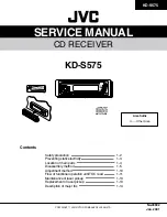
HA13158A (IC321) : Power amp
1. Pin layout
2. Block diagram
IN1
IN2
IN3
IN4
STBY
2
1
11
13
23
10
TAB
PROTECTOR (ASO
SURGE, TSD)
INPUTBUFFER1
INPUTBUFFER2
INPUTBUFFER3
INPUTBUFFER4
AMP1
AMP2
AMP3
AMP4
MUTE
PVCC1
PVCC2
INVCC
+
-
+
-
+
-
+
-
12 22
14 18 6
3
4
5
7
8
9
15
16
17
19
20
21
1 ~ 23
Description of major ICs
Summary of Contents for KD-S575
Page 42: ...KD S575 3 11 M E M O ...