KD-LH1105
(No.49827)1-27
SECTION 4
Description of major ICs
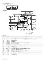
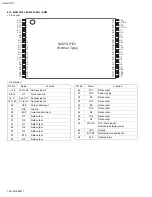
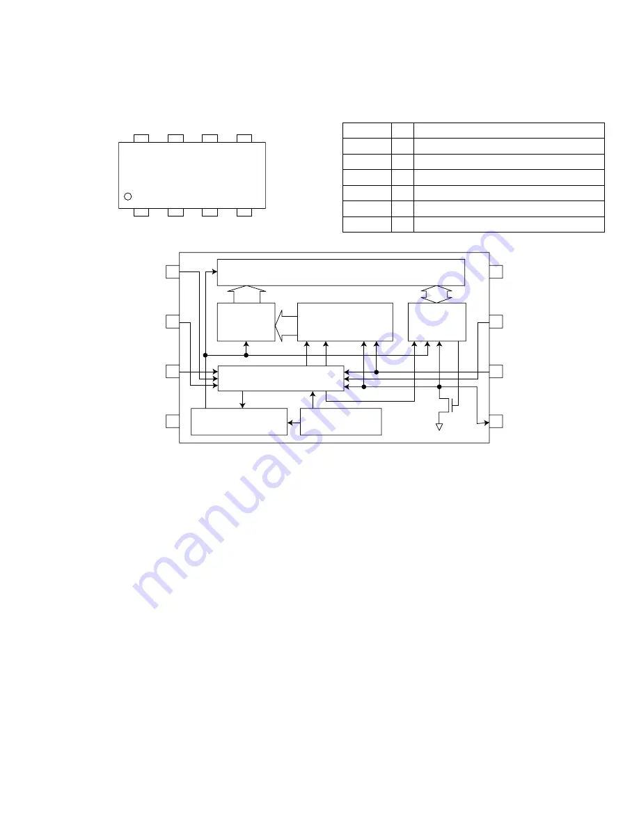
4.1 BR24C16F-X (IC703) : EEPROM
• Pin layout
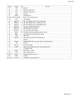
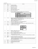
• Pin function
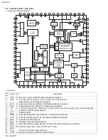
• Block diagram
VCC
WP
SCL
SDA
A0
A1
A2
GND
Symbol
I/O
Function
VCC
- Power
supply.
GND
- GND
A0,A1,A2
I
No use connect to GND.
SCL
I Serial
clock
input.
SDA
I/O Serial data I/O of slave and ward address.
WP
I
Write protect terminal.
8 Vcc
7 WP
6 SCL
5 SDA
A0 1
A1 2
A2 3
GND 4
16kbit EEPROM allay
11bit
11bit
8bit
Address
decoder
Slave Ward
Address resister
Data
resister
START
STOP
ACK
Control circuit
High voltage osc circuit
Power supply
voltage det.
Summary of Contents for KD-LH1105
Page 47: ...KD LH1105 No 49827 1 47 ...

