background image

1-14

UX-P3

Main adjustment

Measurement Instruments Required for

     Adjustment
 
  1. Low frequency oscillator
    This oscillator should have a capacity to output
    0dBs to 600 

 at an oscillation frequency of

    50Hz-20kHz.
  2. Attenuator impedance : 600 
  3. Electronic voltmeter
  4. Distortion meter
  5. Frequency counter
  6. Wow & flutter meter
  7. Test tape
      VTT703L : Head azimuth
      VT712 : Tape speed and running unevenness
                   (3kHz)
      VT724 : Reference level (1kHz)
   8. Blank tape
      TYPE 

: AC-225

      TYPE 

: AC-514

  9. Torque gauge : For play and back tension
      FWD(TW2111A), REV(TW2121a) and
      FF/REW(TW2231A)
10. Test disc: CTS-1000

Radio Input signal

      AM frequency --------------------------------------- 400Hz
      AM modulation ---------------------------------------- 30%
      FM frequency --------------------------------------- 400Hz
      FM frequency deviation ------------------------ 22.5kHz

Tuner section

      B/E/EN version
        FM Band cover:  87.5

108MHz

        MW Band cover: 522

1,629kHz

        LW Band cover:  144

288kHz

      EE version
        FM Band cover:  65

74MHz, 87.5

108MHz

        MW Band cover: 522

1,629kHz

        LW Band cover:  144

288kHz

      UB/UF/US/UX/U version 
        FM Band cover:  87.5

108MHz

        MW Band cover: 531

1,602kHz, 530

1,710kHz

        SW Band cover: SW1 2.3

6.995MHz

                                 : SW2 7

21.85MHz

       Voltage applied to tuner                       +B : DC5.7V
                                                                    VT : DC 12V
      Reference measurement 
        output                                       26.1mV(0.28V)/3
      Input positions             AM : Standard loop antenna
                                      FM : TP1 (hot) and TP2 (GND) 

Standard measurement position of volume

      Function switch                                            to Tape
      Beat cut switch                                               to Cut
      Super Bass/Active hyper Bass                      to OFF
      Bass Treble                                                to Center
      Adjustment of main volume to reference output  
                                                                         VOL : 28
Precautions for measurement
1. Apply 30pF and 33k

to the IF sweeper output

    side and 0.082

F and 100k

in series to the 

    sweeper input side.
2. The IF sweeper output level should be made as 
    low as possible within the adjustable range.
3. Since the IF sweeper is a fixed device, there is no
    need to adjust this sweeper.
4. Since a ceramic oscillator is used, there is no need
    to perform any MIX adjustment.
5. Since a fixed coil is used, there is no need to adjust
    the FM tracking.
6. The input and output earth systems are separated. 
    In case of simultaneously measuring the voltage in
    both of the input and output systems with an 
    electronic voltmeter for two channels, therefore, the
    earth should be connected particularly carefully.
7. In the case of BTL connection amp., the minus
    terminal of speaker is not for earthing. Therefore, be
    sure not to connect any other earth terminal to this
    terminal. This system is of an BTL system.
8. For connecting a dummy resistor when measuring
    the output, use the wire with a greater code size.
9. Whenever any mixed tape is used, use the band
    pass filter (DV-12).

Measurement conditions

 
  Power supply voltage 
                        : AC230V (50Hz)----B/E/EE/EN 
                        : AC110/127V/230V(50/60Hz)
                        : UB/UF/US/UX/U
  Reference output : Speaker : 0.775V/4
                                               : Headphone : 0.077V/32
  Reference frequency and
     input level ------------------------------ 1kHz, AUX : -8dBs
     MIX MIC: -54dBs (UB/UF/US/UX/U)
     Input for confirming recording and playback
             characteristics ------------------------- AUX : -28dBs
     Measurement output terminal ------- at Speaker J3002
     

 Load resistance --------------------------- 4

Summary of Contents for CA-UXP3

Page 1: ...al connection of display 1 2 1 4 1 6 1 7 1 14 1 18 1 19 1 19 1 20 1 39 Area Suffix UB UP US UW UY Hong Kong Korea Singapore South Africa Argentina COMPACT DIGITAL AUDIO CD TAPE FM AM M I C R O C O M P O N E N T S Y S T E M U X P 3 C D R R W P L A Y B A C K AUX TIMER CLOCK STANDBY STANDBY ON VOLUME FUNCTION SOUND DIRECTOPERATING AHBPRO A U T O R E V E R S E AUTO TAPE SELECTOR REC REV MODE PHONES SL...

Page 2: ...et screw heads headphone jack control shafts etc to be sure the product is safe to operate without danger of electrical shock Do not use a line isolation transformer during this check Plug the AC line cord directly into the AC outlet Using a Leakage Current Tester measure the leakage current from each exposed metal parts of the cabinet particularly any exposed metal part having a return path to th...

Page 3: ...amage resulting therefrom 3 Essential safety critical components are identified by on the Parts List and by shading on the schematics and must never be replaced by parts other than those listed in the manual Please note however that many electrical and mechanical parts in the product have special safety related characteristics These characteristics are often not evident from visual inspection Part...

Page 4: ...ng transport and before installation both sides of the laser diode on the replacement optical pickup are shorted After replacement return the shorted parts to their original condition Refer to the text 2 Do not use a tester to check the condition of the laser diode in the optical pickup The tester s internal power source can easily destroy the laser diode 1 2 Handling the traverse unit optical pic...

Page 5: ...2 C673 C676 C677 C679 C680 C691 C692 C693 C694 C695 C696 C699 C801 C802 C811 C812 C813 C814 C815 C821 C822 C823 C824 C831 C832 C833 CN601 CN651 CN652 CN801 D831 R648 IC652 IC801 IC802 L831 Q631 Q801 R601 R602 R603 R604 R605 R606 R610 R611 R612 R613 R617 R618 R619 R620 R621 R631 R632 R634 R635 R636 R641 R642 R643 R647 R651 R652 R653 R654 R655 R656 R657 R658 R659 R661 R662 R663 R664 R665 R666 R667 R...

Page 6: ...fety switches malfunction the laser is able to function 6 CAUTION Use of controls adjustments or performance of procedures other than those specified herein may result in hazardous radiation exposure VARNING Osynlig laserstrålning är denna del är öppnad och spårren är urkopplad Betrakta ej strålen VARO Avattaessa ja suojalukitus ohitettaessa olet alttiina näkymättömälle lasersäteilylle Älä katso s...

Page 7: ...rd and lift the rear part of the cover 1 2 3 Disassembly method Main body Removing the metal cover See Fig 1 and 2 Prior to performing the following procedure remove the metal cover Remove the two screws C on the back of the body 1 Removing the rear cover See Fig 3 Fig 1 Fig 2 Fig 3 A A A A A Metal cover Metal cover B 2 C Rear cover Rear panel C ...

Page 8: ...ws F attaching the rear panel and the CD mechanism on the back of the body Move the rear part of the CD mechanism assembly upwards to disengage the two joints a and release from the rear panel Pull the front panel toward the front and move the rear part of the CD mechanism assembly upwards Then pull out the CD mechanism assembly from the front panel backward 1 2 3 4 Removing the CD mechanism assem...

Page 9: ... as needed 1 2 3 Remove the rear panel See Fig 8 to 11 Prior to performing the following procedure remove the metal cover the rear cover andthe CD mechanism assembly Disconnect the wire from connector CN908 on the main board Remove the two screws H on the back of the body Move the fan upwards to disengage the four joints c and release from the rear panel 1 2 3 Removing the fan See Fig 9 and 12 Fig...

Page 10: ...03 respectively Disconnect the wire from W950 on the underside of the main board Remove the two screws I attaching the main board to the chassis on the left side ofthe body and disengage the two joints c Remove the two screws J attaching the heat sink to the main board 1 2 3 4 Removing the main board heat sink See Fig 13 to 15 Fig 14 Fig 13 Fig 15 Front panel assembly Main board I I Joints c Heat ...

Page 11: ...CD mechanism assembly and the rear panel Disconnect the card wire from connector CN900 CN901 and CN931 on the main board Refer to Fig 13 Disconnect the wire from CN906 and FW903 respectively Refer to Fig 13 Disconnect the wire from W950 on the underside of the main board Remove the two screws L on each lower side of the body Release the lower joints d on each side of the body using a screwdriver P...

Page 12: ...d Remove the screw N attaching the switch board to the LCD holder If necessary unsolder the wire extending from connector FW931 on the display board and FW931 on the switch board If necessary remove the band bundling the wires extending from the headphone board and the display board 1 2 3 4 5 Removing the display board switch board See Fig 20 to 22 Front panel assembly VOLUME knob Display board Sw...

Page 13: ...rd 1 2 Removing the headphone board See Fig 23 Prior to performing the following procedure remove the front panel assembly Press the EJCT button on the front panel to open the cassette door Remove the four screws P on the back of the front panel 1 2 Removing the cassette mechanism assembly See Fig 23 and 24 Fig 23 Fig 24 Display board P Band O Headphone board Cassette mechanism assembly P Front pa...

Page 14: ...Center Adjustment of main volume to reference output VOL 28 Precautions for measurement 1 Apply 30pF and 33k to the IF sweeper output side and 0 082 F and 100k in series to the sweeper input side 2 The IF sweeper output level should be made as low as possible within the adjustable range 3 Since the IF sweeper is a fixed device there is no need to adjust this sweeper 4 Since a ceramic oscillator is...

Page 15: ...1 10 CN32 9 1IC31 8 9 IC32 1 16 16 1 8 9 IC33 L301 Q101 Q201 Q305 Q302 B168 C334 B Q375 E Q376 Q371 B E C201 R101 R102 C104 R105 R106 R107 R108 C221 R110 R111 R112 R121 R201 R202 C204 R205 R206 R207 R208 C111 R210 R211 R212 R221 R301 R303 R304 B167 R335 R315 R314 R313 R310 R122 Q103 R305 B151 R371 R375 R376 R372 R338 R337 R341 R342 R343 R339 R336 R331 VR31 VR37 C210 C110 C102 C101 Q372 C213 C211 R...

Page 16: ...ly when the head has been changed Test tape VT712 3kHz Measurement output terminal Headphone terminal When the test tape VT712 3kHz has been played back with the recording and playback mechanism at the beginning of forward winding the frequency counter reading of the difference between both of the mechanism should be 6 0Hz or less Adjust VR37 so that the frequency counter reading becomes 2 940 3 0...

Page 17: ... mechanism to the recording and pausing condition in advance 2 While repetitively inputting the reference frequency signal of 1kHz and 10kHz from OSC IN record and playback the rape 3 While recording and playback the test tape in TYPE adjust VR31 for Lch and VR32 for Rch so that the output deviation between 1kHz and 10kHz becomes 1dB 2dB 1 While recording and playback mechanism load the test tapes...

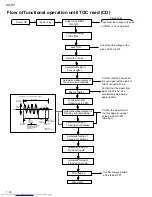
Page 18: ...es Automatic measurement of TE amplitude and automatic tuning of TE balance 500mv div 2ms div Fig 1 Approx 3sec pin 20 of IC601 TE Approx 1 8V VREF Tracking error waveform at TOC reading Power ON Power Key Confirm that the Focus error S cuve siganl at the pin23 of IC601 is approx 2Vp p Confirm that the siganl from pin22 IC603 is 0V as a accelerated pulse during approx 400ms Confirm the waveform of...

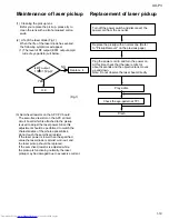
Page 19: ...the life of the laser diode has expired the following symptoms wil appear 1 The level of RF output EFM output ampli tude of eye pattern will below Is RF output 1 1 0 15Vp p Replace it NO YES O K 3 Semi fixed resistor on the APC PC board The semi fixed resistor on the APC printed circuit board which is attached to the pickup is used to adjust the laser power Since this adjustment should be performe...

Page 20: ...AUX _PBMUTE _SMUTE SPKMUTE _AHB P_OUT PROTR MODEL1 MODEL2 I I I O O I O I O O O O O O O I I O O O O O O O O O I I Irregular voltage detection 0 REST CLOSE switch detect port CD safety voltage detect port CD speed control CD Gain Control Q code data input port Q code serial clock CD status input port CD data input port CD data clock CD reset CD command ready signal BTL mute control port Serial Date...

Page 21: ..._MPX BCTL BLKCK SAFETY1 TAPE0 TAPE1 KEY1 KEY2 O O O O O O O I O O O I O I I I O O O I I I O I I I I I I Lite LED indicate Reverse Lite LED indicate REC Lite LED indicate Forward Tape IC Strobe LCD data LCD date mode control LCD clock Tape End Detection LCD Driver inhibit L at end of tran LCD driver chip enable LCD DIM Control Volumn Plus Power Standby LED control Bass Minus Volumn Minus Bass plus ...

Page 22: ...lifier outputs ON OFF BTL AMP 1 input pin BTL AMP 1 input pin For gain adjustment BTL AMP 1 input pin Non inverting side BTL AMP 1 input pin Inverting side BTL AMP 2 input pin Inverting side BTL AMP 2 input pin Non inverting side BTL AMP 2 input pin For gain adjustment BTL AMP 2 input pin External transistor collector PNP connection 5V power supply output External transistor PNP base connection Re...

Page 23: ... MDATA DSL PLL VCO AVDD2 SUB CODE BUFFER SSEL SQCK SUBQ AVDD2 CLVS CRC BLKCK CLDCK SBCK SUBC DEMPH RESY FLAG6 RESY EFM DEMODULATION SUBCODE DEMODULATION SYNC INTERPOLATION 16k SRAM CIRC ERROR CORRECTION DEINTERLEVE LRCKIN MSEL BCLK SSEL SRDATAIN PSEL IOSEL DIGITAL DEEMPHSIS 8TIMES OVER SAMPUNC DIGITAL FILTER 1BIT DAC LOGIC S PEM R PEM L DIGITAL AUDIO INTERFASE DIGITAL AUDIO INTERFASE INTER POLATIO...

Page 24: ...al output Kick pulse output Tracking drive output Focus drive output Reference voltage input pin for D A output block TVD FOD FBA TBAL Focus Balance adjust signal output Tracking Balance adjust signal output Focus error signal input Analog input Tracking error signal input Analog input RF envelope signal input Analog input Vibration detect signal input H detect Off track signal input H off track T...

Page 25: ...IN2 OUT1 1 IN1 2 IN1 3 VEE 4 BA15218F XE IC904 Dual operation amplifier 1 Pin layout 2 Block diagram Q19 Q17 Q16 OTHER CH R9 R6 R8 R7 R5 R4 R3 R2 R1 D1 C1 Q18 Q13 Q11 Q8 Q5 Vcc VEE OUTPUT IN IN Q1 Q3 Q4 Q2 C2 Q9 Q6 Q7 Q10 Q12 Q14 Q15 Q114 ...

Page 26: ...1 26 UX P3 Q14 Q12 Q13 Q10 Q11 Q4 Q3 Q5 Q6 Q1 Q2 Q7 Q8 Q9 Z1 R9 R3 R4 R1 R2 R8 R7 R5 R6 Q16 R11 R10 C1 3 INPUT 1 OUTPUT 2 COMMON KIA78S06P T IC933 Regulator 1 Pin layout 2 Block diagram 1 2 3 ...

Page 27: ...1 27 UX P3 1 Pin layout LA4628 IC905 Power amp 1 2 3 4 5 6 7 8 9 10 11 12 13 14 2 Block diagram RF Vcc OUT GND1 OUT OUT GND2 OUT NC PP IN1 SG STB IN2 ...

Page 28: ...EOUT TEN FEN FEOUT GCTL FBAL TBAL E F D B C A Earth terminal VREF output terminal VDET output terminal VDET input terminal TE Amp output terminal TE Amp reversing input terminal FE Amp reversing input terminal FE Amp output terminal Terminal GCTL APC FBAL control terminal TBAL control terminal Tracking signal input terminal 1 Tracking signal input terminal 2 Focus signal input terminal 4 Focus sig...

Page 29: ... AM OSC REG AM RF AFC AM AGC O I O I I I AM Local oscillation Signal output This is a terminal of AM Local oscillation circuit Register value between pin 26 and pin28 desides the frequency width of the input signal AM RF signal input This is an output terminal of voltage for FM AFC This is an AGC voltage input terminal for AM O O I O AM detection output FM detection output Mpx input terminal O O I...

Page 30: ...output port Input output port Data input output Function IF counter signal input IF signal output Not use AM Local OSC signal output FM Local OSC signal input Power suplly VDD 4 5 5 5V When power ON Reset circuit move PLL charge pump output H Local OSC frequency Height than Reference frequency L Low Agreement Height impedance Input for active lowpassfilter of PLL Output for active lowpassfilter of...

Page 31: ... VREF MPXIN Vdda Vssa FLOUT CIN TEST XOUT XIN Vssd Vddd MODE RST RDDA RDCL RDS ID READY I O O O O O O I I I I I I I O Reference voltage output Vdda 2 Baseband multiplexed signal input Analog power supply 5V Analog ground Subcarrier input comparator input Subcarrier input filter output Test input Crystal oscillator input exeternal reference input Crystal oscillator output 4 332MHz Digtal ground Dig...

Page 32: ...B1641 IC802 DC Motor driver 1 Pin layout 2 Pin function STROBE DATA CLOCK Q1 Q2 Q3 Q4 Vss Vdd OUTPUT ENABLE Q5 Q6 Q7 Q8 Q s Qs 1 2 3 4 5 6 7 8 16 15 14 13 12 11 10 9 1 Pin layout 8 STAGE SHIFT REGISTER 8 BIT LATHES 3 STATE OUTPUTS 1 2 3 15 Q1 Q8 10 9 DATA CLOCK STROBE OUTPUT ENABLE PARALLEL OUTPUT Q s Qs SERIAL OUTPUT 2 Block diagram BU4094BC IC33 Serial to parallel port extension ...

Page 33: ...1 33 UX P3 GP1U26X IC933 BA3126N IC31 R P Switch R E C S W G 1 2 3 4 5 6 7 8 9 P B S W P B S W G R E C S W C O N T G N D V c c ...

Page 34: ...mon Driver Latch Circuit Segment Driver Divider Circuit Oscillation Circuit Input Switching Circuit Shift Register 4 Input Switching Circuit Input Switching Circuit Input Switching Circuit Shift Register 3 Shift Register 2 Shift Register 1 Input Seiector Circuit Decoder Shift Register Control Circuit 2 Bock diagram ...

Page 35: ...1 35 UX P3 1 Pin layout LC75345M IC901 2 Block Diagram ...

Page 36: ...lector output pin LBASS1 LBASS2 RBASS1 RBASS2 LSB RSB 10 9 28 29 8 30 Capacitor and resistor connection pins comprising filters for bass and super bass band LOUT ROUT 7 31 ATT equalizer output pin capacitor connection pin comprising filter for super bass LVRIN RVRIN 12 26 Volume input pin LTRE RTRE 11 27 Capacitor connection pin comprising treble band filter ...

Page 37: ...onnect between pins 33 and 34 LOPOUT ROPOUT 4 34 0 5 VDD voltage generation block for analog ground Capacitor of several 10 F to be connected between Vref and AWSS VSS as a counter measure against power ripple VSS 3 Ground pin VDD 35 Supply pin CE 2 Chip enable pin Data written into an internal latch in a timing of H L Each analog switch is activated Data transfer enabled at H level Non inverted i...

Page 38: ...1 38 UX P3 AN7317 IC32 PB REC amp ...

Page 39: ...1 39 UX P3 QLD0160 001 D1934 Internal connection of display ...

Page 40: ...1 40 UX P3 MEMO ...

Page 41: ...1 41 UX P3 200106 O No 20984 UX P3 VICTOR COMPANY OF JAPAN LIMITED AUDIO COMMUNICATION BUSINESS DIVISION PERSONAL MOBILE NETWORK BUSINESS UNIT 10 1 1Chome Ohwatari machi Maebashi city 371 8543 Japan ...

Reviews: