


NSVS850 Apr. 2005
1
3
4
5
6
2
(1.35)
(0.8)
(
0
.55)
(0
.6
)
1.
1
±
0.
1
3.2±0.1
2.
5
±
0.
1
(1)
(b)
(2)
(a)
[4x]
[4
x
]
[2
x
]
[2x]
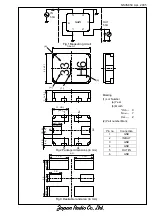
Marking
(1) Lot Number
(a)
Year
(b)
Month
*Oct.---
X
Nov.---
Y
Dec.---
Z
(2) Part number Mark
Pin no.
Connection
1 GND
2 IN/OUT
3 GND
4 GND
5 OUT/IN
6 GND
Fig.1 Measuring circuit
Fig.2 Package dimensions (in mm)
Fig.3 Desirable land area (in mm)
H6
33
1
2
3
4
5
6
SAW
0.
95
0.
6
0.
95
3.
3
1.75
1.75
4.0
1.2
IN
50
Ω
OUT
50
Ω


