NJU39612
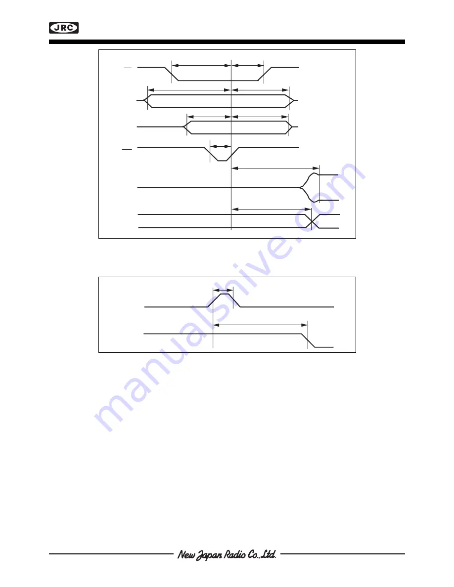
Figure 8. Timing
Figure 9. Timing of Reset
t
CS
A0
D0-D7
WR
DA
Sign
cs
ch
as
ah
ds
dh
DAC
pwr
Reset
res
pres
Page 1: ...ivers Package EMP20 BLOCK DIAGRAM NJU39612E2 NJU39612 is a dual 7 bit sign Digital to Analog Converter DAC developed to be used in micro stepping applications together with the dual stepper motor driv...
Page 2: ...o set data bit 5 in data word 9 D4 Data 4 TTL CMOS level input to set data bit 4 in data word 10 D3 Data 3 TTL CMOS level input to set data bit 3 in data word 11 D2 Data 2 TTL CMOS level input to set...
Page 3: ...g time requires zero to full scale or full scale to zero output change Settling time is the time required from a code transition until the DAC output reaches within 1 2 LSB of the final output value F...
Page 4: ...drop from pin to resistor Any VRef between 0 0 V and VDD can be applied but output might be non linear above 3 0 V Power on Reset This function automatically resets all internal flip flops at power o...
Page 5: ...5 3 8 V Rise and fall time of WR tr tf 1 s ABSOLUTE MAXIMUM RATINGS Parameter Pin no Symbol Min Max Unit Voltage Supply 4 VDD 6 V Logic inputs 5 14 16 VI 0 3 VDD 0 3 V Reference input 1 VRef 0 3 VDD...
Page 6: ...ycle length tWR 50 ns Reset cycle length tres 80 ns Reference Input Input resistance Rref 6 9 kohm Logic Outputs Logic HIGH output current IOH VO 2 4 V 13 5 mA Logic LOW output current IOL VO 0 4 V 2...
Page 7: ...NJU39612 Figure 8 Timing Figure 9 Timing of Reset t t t t t t t CS A0 D0 D7 WR DA Sign cs ch as ah ds dh WR t DAC tpwr t t Reset Sign res pres...
Page 8: ...it is heavily loaded with other tasks With a microprocessor data is stored in ROM RAM area or each step is successively calculated NJU39612 is connected like any peripheral addressable device All part...
Page 9: ...Time Time when motor is in an intermediate position Time when micro position is almost correct Write signal Motor position Note that position is always a compromise Writing to channel 1 Writing to cha...
Page 10: ...ulses to the device with the correct addressing in between keeping the delay between the pulses as short as possible Write signals will look as illustrated in figure10 The advantages are low torque ri...
Page 11: ...n DA 1 1 NJU39612 Voltage Reference Control Logic Step Direction Clock Up Dn CE A0 WR CS Vref D0 D7 Counter PROM NJU39612 NJM3777 Figure 13 Typical application in a microprocessor based system Figure...