background image


User’s Manual


20 


The functions of 

COM9/COM10 will vary according to Jumpers’ setting. JP9/JP10/JP11/JP12 allow you 

to configure the serial COM9/10 to RS232

RS422 or RS485; JP13 allows you to select the power supply 

RI/5V/12V. Refer to “2.3.3”,”2.3.4”,”2.3.5” chapters for more information. 

Table 2.8 for pin assignments. 

Table 2.8: COM9/10 Serial Port Pin Assignments   

Pin 

RS-232 Signal 

RS-422 Signal   

RS-485 Signal   

1   

DCD   

TX- 

DATA- 

2   

RxD   

TX+ 

DATA+ 

3   

TxD   

RX+   

NC 

4   

DTR   

RX-   

NC 

5   

GND   

GND   

GND   

6   

DSR   

NC   

NC   

7   

RTS   

NC   

NC   

8   

CTS   

NC   

NC   

9   

RI/5V/12V   

NC 

NC 


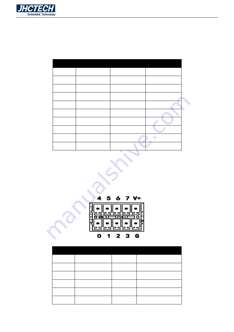
2.4.9 DIO Connector 

The KMDA-2702 provides a 16-bit DIO by two 2*5Pin 8-bit DIO terminal connectors in rear. Table 2.9 

for pin assignments. 


Figure 2.22 8-bit DIO Connector 

Table 2.9: DIO Pin Assignments   

Pine 

DIO Signal   

Pin 

DIO Signal 

1   

DIO0 

DIO4 

2   

DIO1 

DIO5   

3   

DIO2 

DIO6 

4   

DIO3 

DIO7   

5   

GND 

10 

VCC 


Summary of Contents for KMDA-2702

Page 1: ...User s Manual 1 User s Manual KMDA 2702 Ver A1 0 Date 15 October 2018 ...

Page 2: ...User s Manual 2 Version Note No Ver Note Date Writer 1 A1 0 first publish 20180815 Tracy Liu ...

Page 3: ...ntended to be accurate and reliable However Shenzhen JHC Technology Co Ltd assumes no responsibility for its use nor for any infringements of the rights of third parties which may result from its use Acknowledgements Award is a trademark of Award Software International Inc IBM PC AT PS 2 and VGA are trademarks of International Business Machines Corporation Intel and Pentium are trademarks of Intel...

Page 4: ...ent materials service time and freight Please consult your dealer for more details If you think you have a defective product follow these steps 1 Collect all the information about the problem encountered For example CPU speed JHC products used other hardware and software used etc Note anything abnormal and list any onscreen messages you get when the problem occurs 2 Call your dealer and describe t...

Page 5: ...nce when the equipment is operated in a commercial environment This equipment generates uses and can radiate radio frequency energy and if not installed and used in accordance with the instruction manual may cause harmful interference to radio communications Operation of this equipment in a residential area is likely to cause harmful interference in which case the user will be required to correct ...

Page 6: ... resistor Select Jumper 13 2 3 5 COM9 COM10 RI 5V 12V Power supply Select 13 2 4 I O BUTTON AND LED INDICATION 14 2 4 1 Ethernet Connector LAN 15 2 4 2 Power Input Connector DC IN 15 2 4 3 USB Connector 16 2 4 4 HDMI 17 2 4 5 VGA Connector 18 2 4 6 COM1 2 5 6 7 8 Connector 18 2 4 7 COM3 4 Connector 19 2 4 8 COM9 10 Connector 19 2 4 9 DIO Connector 20 2 4 10 SATA2 0 Port connector 21 2 4 11 SATA Po...

Page 7: ...3 2 6 Security Menu 51 3 2 7 Save Exit Menu 52 3 3 UPDATING THE BIOS 52 DRIVER INSTALLATION 54 4 1 ABOUT THE SOFTWARE DVD ROM CD ROM 55 4 2 AUTO INSTALLING UNDER WINDOWS 8 10 55 4 3 MANUAL INSTALLATION 58 4 4 CPU TEMP LED DRIVER 59 4 5 UTILITY SOFTWARE REFERENCE 59 SYSTEM RESOURCE 60 5 1 WDT AND GPIO 61 5 1 1 WDT 61 5 1 2 GPIO 62 ...

Page 8: ...User s Manual 1 General Information CHAPTER 1 ...

Page 9: ...ATA for storage DC 9 36V wide power input Besides operating temperature showing in LEDs economic and reliable it will be fit for security and manufacture application 1 2 Features Key features 1 Universal Aluminum chassis Fanless design 2 Intel Celeron Processor J1900 2 0 2 42G CPU 3 1 DDR3L 1333MHz SODIMM Up to 8GB 4 3 Intel I211 AT PCIe Gig LAN 5 1 Mini PCIe with PCIeX1 USB signal Full size 1 Min...

Page 10: ...1 3 2 Display Chipset Intel HD Graphics Display Memory Shared system memory Resolution HDMI up to 1920x1080 60Hz VGA up to 1920x1200 60Hz 1 3 3 Ethernet Chipset 3 Intel I211AT PCI Express Gigabit Ethernet controller Speed 10 100 1000 Mbps Integrated Interface 3 RJ45 1 3 4 Audio Chipset Realtek ALC662VD Interface 1 Line out 1 Mic 3 5mm phone jack 1 3 5 Power Consumption Input Voltage DC 9 36V Input...

Page 11: ... With HDD 1 Grms random 5 500 Hz Shock during operation With SSD 50g peak acceleration 11 ms duration With HDD 20g peak acceleration 11 ms duration EMC CE FCC Class A 1 5 Mechanical Specifications The KMDA 2702 Fanless Embedded Box Computer contains an JHC SBC Single Board Computer board an JHC sub board and an JHC sub card that is housed in an aluminum plate chassis Main board front Figure 1 0 ...

Page 12: ...User s Manual 5 Main board rear Figure 1 1 Sub board ECB 153 Figure 1 2 ...

Page 13: ...User s Manual 6 Sub card ECD 7150 Figure 1 3 KMDA 2702 Dimensions Uint mm Figure 1 4 ...

Page 14: ...User s Manual 7 Hardware Installation CHAPTER 2 ...

Page 15: ... Fanless Embedded Box Computer consists of an JHC SBC Single Board Computer board an JHC sub board and an JHC sub card that is housed in an aluminum plate chassis Warning Do not remove any mechanical parts until you have verified that no power is flowing within the Embedded Box Computer Power must be switched off and the power cord must be unplugged JHC SBC board Internal Diagram Figure 2 1 ...

Page 16: ... consists of two metal pins and a small metal clip often protected by a plastic cover that slides over the pins to connect them To close a jumper you connect the pins with the clip To open a jumper you remove the clip Sometimes a jumper will have three pins labeled 1 2 and 3 In this case you would connect either pins 1 and 2 or pins 2 and 3 Figure 2 3 The jumper settings are schematically depicted...

Page 17: ...pers have a white arrow next to pin 1 2 3 Jumper Location The KMDA 2702 Embedded Box Computer has a number of jumpers inside the chassis that allows you to configure your system to suit your application The table below lists the functions of the various jumpers The table below shows the function of each of the board s jumpers Figure 2 5 Jumpers Jumper Name Description CMOS Clear CMOS Data Setting ...

Page 18: ...can reconfigure the system with the default values stored in the ROM BIOS To load the default values stored in the ROM BIOS please follow the steps below 1 Power off the system and unplug the power cord 2 Set CMOS pins 2 and 3 to On Wait for a few seconds and set CMOS back to its default setting pins 1 and 2 On 3 Now plug the power cord and power on the system ...

Page 19: ...Power supply 12V 5V 3 3V Mode Select Figure 2 7 J_PANEL is used to select the power supplied of LVDS panel 2 3 3 COM5 6 7 8 9 10 RS232 RS485 RS422 Mode Select Figure 2 8 NOTE JP1 JP3 JP5 JP7 JP9 JP11 corresponds to COM5 6 7 8 9 10 ...

Page 20: ...7 8 9 10 Matching resistor Select Jumper Figure 2 9 NOTE JP2 JP4 JP6 JP8 JP10 JP12 corresponds to COM5 6 7 8 9 10 2 3 5 COM9 COM10 RI 5V 12V Power supply Select Figure 2 10 NOTE Pin 12 and 34 are for COM9 Pin 56 and 78 are for COM10 ...

Page 21: ...User s Manual 14 2 4 I O Button and LED indication Front view Figure 2 11 Rear view Figure 2 12 ...

Page 22: ...or Table 2 1 RJ 45 Connector pin assignments Pin 10 100 1000BaseT Signal 1 TX 10 100 LAN_DA GHz 2 TX 10 100 LAN_DA GHz 3 RX 10 100 LAN_DB GHz 4 LAN_DC GHz 5 LAN_DC GHz 6 RX 10 100 LAN_DB GHz 7 LAN_DD GHz 8 LAN_DD GHz 2 4 2 Power Input Connector DC IN The KMDA 2702 uses a power socket that supports up to 60W of power and is a low power solution Using a 12V adapter to input voltage and a DC power su...

Page 23: ... The USB interface connector is used for connecting any device that con forms to the USB interface Many recent digital devices conform to this standard The USB interface supports Plug and Play which enables you to connect or disconnect a device whenever you want without turning off the computer The USB2 0 pin definition is as follows Figure 2 15 USB2 0 connector Table 2 2 USB2 0 Connector Pin Sign...

Page 24: ...a high resolution HDMI display port it supports the most resolution up to 1920 1080 60Hz Table 2 4 for pin assignments Figure 2 17 HDMI Connector Table 2 4 HDMI Pin Assignments Pin Signal Pin Signal Pin Signal 1 DATA2_P 8 GND 15 SCL 2 GND 9 DATA0_N 16 SDA 3 DATA2_N 10 CLK_P 17 GND 4 DATA1_P 11 GND 18 VCC 5 GND 12 CLK_N 19 DETECT 6 DATA1_N 13 NC 7 DATA0_P 14 NC Note NC represents No Connection ...

Page 25: ... 5 GND 13 HS 6 GND 14 VS 7 GND 15 SCL 8 GND Note NC represents No Connection 2 4 6 COM1 2 5 6 7 8 Connector The KMDA 2702 provides 6 serial ports of COM1 2 5 6 7 8 by 6 D sub 9 pin connectors COM1 2 can be configured as RS232 RS422 or RS485 by BIOS setup COM5 6 7 8 can be configured as RS232 RS422 or RS485 by jumpers setting Table 2 6 for pin assignments Figure 2 19 COM1 2 Connector Table 2 6 COM1...

Page 26: ...s No Connection 2 4 7 COM3 4 Connector Figure 2 20 COM3 4 Connector COM3 4 are only for RS232 Table 2 7 for pin assignments Table 2 7 COM3 4 Serial Port Pin Assignments Pin Signal Pin Signal 1 DCD 2 RxD 3 TxD 4 DTR 5 GND 6 DSR 7 RTS 8 CTS 9 RI 2 4 8 COM9 10 Connector Figure 2 21 COM9 10 Connector ...

Page 27: ...Table 2 8 COM9 10 Serial Port Pin Assignments Pin RS 232 Signal RS 422 Signal RS 485 Signal 1 DCD TX DATA 2 RxD TX DATA 3 TxD RX NC 4 DTR RX NC 5 GND GND GND 6 DSR NC NC 7 RTS NC NC 8 CTS NC NC 9 RI 5V 12V NC NC 2 4 9 DIO Connector The KMDA 2702 provides a 16 bit DIO by two 2 5Pin 8 bit DIO terminal connectors in rear Table 2 9 for pin assignments Figure 2 22 8 bit DIO Connector Table 2 9 DIO Pin ...

Page 28: ...assignments Figure 2 23 Table 2 10 SATA Port Pin Assignments Pin Signal Pin Signal 1 GND 5 RX 2 TX 6 RX 3 TX 7 GND 4 GND 2 4 11 SATA Power Connector Figure 2 24 Table 2 11 SATA Power Pin Assignments Pin Signal Pin Signal 1 5V 3 GND 2 GND 4 12V Warning Make sure that Pin 1 of compatible SATA Power connector is inserted into corresponding Pin 1 of PWOUT to avoid possible damage to the board and hard...

Page 29: ...ine Out connector and a Mic connector for audio output and input 2 4 14 Remote Switch signal Connector For the remote switch signal interface of the switch machine the terminal of the motherboard coastline is a 2 pin terminal as shown below Figure 2 26 Table 2 13 Remote Switch Pin Assignments Pin Type Signal 1 PWR_BTN 2 GND 2 4 15 AT ATX SW The KMDA 2702 provides a AT ATX SW which users can set Po...

Page 30: ...of the DC IN on the front panel Unscrew 6 serial copper columns and 5 screws on the front panel Step 4 remove the front panel and the bottom cover Step 5 Put the HDD SSD in the drive bay and screw 4 screws Step 6 Pull the drive bay onto the bottom cover and screw 4 screws Step 7 Using the SATA cable connect the HDD SSD with the mother board Step 8 Close the bottom cover back to the chassis install...

Page 31: ...User s Manual 24 Figure 2 28 Figure 2 29 Figure 2 30 ...

Page 32: ...User s Manual 25 Figure 2 31 Figure 2 32 Figure 2 33 ...

Page 33: ...User s Manual 26 Figure 2 34 Figure 2 35 Figure 2 36 ...

Page 34: ...al copper columns on the front panel Unlock the spring pad and nut of the DC IN on the front panel remove the front panel Rotate the bottom assembly 180 separate the SATA cable which connected the HDD SSD with the mother board Unscrew 6 screws and 16 serial copper columns on the rear panel remove the rear panel Unscrew 7 screws on the sub board remove the sub board Figure 2 37 Figure 2 38 ...

Page 35: ...User s Manual 28 Figure 2 39 Figure 2 40 Figure 2 41 ...

Page 36: ...User s Manual 29 Figure 2 42 Figure 2 43 Figure 2 44 ...

Page 37: ...re 2 46 Step 4 Install the sub card on the mainboard Screw 7 screws on the sub card Install the front panel Screw 5 screws and 6 serial coppers on the front panel lock the nut and spring pad of the DC IN Install the rear panel Screw 6 screws and 16 serial coppers on the rear panel Connect the HDD SSD to the mainboard with the SATA cable Close the bottom cover back to the chassis screw 2 screws on ...

Page 38: ...User s Manual 31 Figure 2 47 Figure 2 48 Figure 2 49 ...

Page 39: ...User s Manual 32 Figure 2 50 Figure 2 51 Figure 2 52 ...

Page 40: ...p 2 Hold the MSATA module with its notch aligned with the MSATA socket of the board and insert it at a 30 degrees angle into the socket as shown in the picture Figure 2 53 Step 3 Screw one screw to the holder as shown in the picture Figure 2 54 Step 4 The step here is the same as above chapter 2 5 2 Installing Mini PCIe Module Step 4 For details please refer to the above chapter 2 5 2 Installing M...

Page 41: ...User s Manual 34 BIOS Setup CHAPTER 3 ...

Page 42: ...ally transfer to the SETUP setting screen after detecting the IDE and other devices 1 Turn on the system or restart the system The self test message will appear on the display screen 2 When the Press Del to enter setup prompt appears in the middle of the screen press the Del key to enter the BIOS setup program 3 Use the arrow keys to move to the option you want to modify and press Enter to enter t...

Page 43: ...stem information Select an item and press Enter to display the submenu Figure 3 1 BIOS Vendor American Megatrends This item shows the information of the BIOS vendor BIOS ID JH715A14 This item shows the information of the BIOS version OS Selection Windows 7 This item shows the OS Selection Build Date and Time 02 05 2018 19 26 45 This item shows the information of the BIOS build date and time System...

Page 44: ...up more advanced information about your system Handle this page with caution Any changes can affect the operation of your computer Figure 3 2 ACPI Settings The item in the menu shows the highest ACPI sleep state when the system enters suspend Figure 3 3 ...

Page 45: ...he Advanced Menu page IT8786 Supper IO Configuration The item in the menu shows the information of RTC wake settings Figure 3 4 Serial Port 1 Configuration Serial Port 1 Settings Serial Port 2 Configuration Serial 2 Settings Serial Port 3 Configuration Serial Port 3 Settings Serial Port 4Configuration Serial Port 4 Settings 8 bit TTL GPIO input and output settings Serial Port 1 Configuration ...

Page 46: ...d on or off The setting value is Enabled Disabled Device Setting Read Only This item displays the interrupt and address of the serial port Change Setting Set port interrupt and address of the serial port Serial MODE Set the mode of the serial port Subcard IO used with the subcard ECB 154 Figure 3 6 ...

Page 47: ...erial Port 5 10Configuration Serial Port 5 10 Configuration is the same as above H W Monitor PC Health Status This item is used for hardware security detection The BIOS will display the current CPU and system temperature Figure 3 8 ...

Page 48: ...ther to power on regularly The setting value is Enabled Disabled If you select Enabled set the hour minute and second in the pop up options Serial Port Console Redirection Figure 3 10 Console Redirection Use this item to Serial Port Console Redirection Press Esc to return to the Advanced Menu page ...

Page 49: ...information including model number CPU family cache size clock speed and brand as well as transistor number pin type size etc In the BIOS setup options of the Intel platform it is usually Limit CPUID MAX to 3 The meaning is limit the execution of the CPUID instruction to return a value greater than 3 Because return values greater than 3 may cause some operating system wrong generally set this opti...

Page 50: ... system hypothesis technology used in Intel s CPU It enables multiple OS to run on a single PC VT technology will play a very important role in various types of processors including dual core processors This technology enables the processor to have and or virtualization technology With Virtualization Technology we can run two operating systems simultaneously on the same machine Power Technology Th...

Page 51: ...rn to the Advanced Menu page SATA ODD Port This item indicates which SATA port is set as the optical drive port SATA Mode This item is used to set the operating mode of the SATA Serial ATA Port 0 This item shows whether to shut down Serial ATA Port 0 SATA Port 0 Hotplug This item shows whether supports SATA Port 0 Hotplug Serial ATA Port 1 This item shows whether to shut down Serial ATA Port 1 SAT...

Page 52: ... the activation status all the time Option ROM Messages This item shows the display mode of option ROM Message Boot option filter This item indicates the boot priority of controlling EFI or Legacy OpROM Network This item is used to set the EFI network card OpROM boot or the traditional network card OpROM boot or priority boot Storage This item is used to set the EFI storage OpROM boot or the tradi...

Page 53: ...herwise select Disabled USB 2 0 EHCI Support Enabled Allows USB EHCI transport protocol with a maximum transfer rate of 480Mpbs Disabled Disable the USB2 0 interface the traditional transfer rate is 12Mpbs USB 2 0 Controller Mode This item sets USB 2 0 device works in full speed mode FullSpeed or high speed mode HiSpeed EHCI Hand off This option is used to determine whether to cut the USB port int...

Page 54: ... 20 seconds Device Power up Delay This item sets the maximum delay time that the USB device reports to the primary controller Mass Storage Devices This item is used to set the specific type of connected USB device The setting value is Auto Floppy Forced FDD Hard Disk CD ROM the default is Auto 3 2 4 Chipset Menu The chipset menu items allow you to change the settings for the North Bridge chipset S...

Page 55: ...integrated graphics is enabled Primary Display This item shows the main output display device when the system starts up DVMT pre AIIocated This item sets the memory size pre assigned to the motherboard integrated graphics in DVMT mode DVMT Total Gfx Mem This item shows how much dynamic memory is allocated to the integrated graphic in total LCD Control Figure 3 18 ...

Page 56: ...screen Press Esc to return to the Chipset Menu page South Bridge Scroll to this item and press Enter and view the following screen Figure 3 19 Restore AC Power Loss This item sets the power on status after power on If Power Off is selected you need to press the power button to power on after power on If Power On is selected it will be powered on directly after power on If Last State is selected af...

Page 57: ...k State This item determines if the NumLock key is active or inactive at system start up time The default value is On which is a digital lock on when the system starts Set to Off the keypad is in cursor control state at startup Show Full Logo This item shows the vendor logo on the startup screen Enabled Display static LOGO screen at startup Disabled Display self test information at start Boot Opti...

Page 58: ...can be used as the boot device If there are multiple hard disks you should select the priority of these hard disks in the item The highest priority hard disk will be displayed in Boot Option 1 3 2 6 Security Menu Scroll to this item and press Enter and view the following screen Figure 3 22 ...

Page 59: ...d Output System Setup Utility displays the system s configuration status and provides you with options to set system parameters The parameters are stored in battery backed up CMOS RAM that saves this information when the power is turned off When the system is turned back on the system is configured with the values you stored in CMOS The BIOS provides the underlying driver for hardware resources an...

Page 60: ...xxxxx bin If you need to add other parameters after the instruction please add space after the above instruction NOTE 1 Only upgrade the BIOS if you encounter problems and need to 2 To upgrade the BIOS please use the BIOS read write program attached to our driver CD or download the updated version of the program from the relevant website 3 Do not turn off the power or reboot the system during the ...

Page 61: ...User s Manual 54 Driver Installation CHAPTER 4 ...

Page 62: ...mation that is not included in this manual Never try to install all software from folder that is not specified for use with your motherboard 4 2 Auto installing under Windows 8 10 The Auto install DVD ROM CD ROM makes it easy for you to install the drivers and software for your motherboard If the Auto install DVD ROM CD ROM does not work on your system you can still install drivers through the fil...

Page 63: ...different operating systems such as Windows 7 8 10 Always go to the correct folder for the kind of OS you are using In install the software execute a file named SETUP EXE by double clicking the file and then following the instructions on the screen The Exit button closes the Auto Setup window Utilities Tab Lists the software utilities that are available on the disk Information Tab Displays the pat...

Page 64: ...lation screen appears Figure 4 2 5 Follow the instructions on the screen to install the items Drivers and software are automatically installed in sequence Follow the onscreen instructions confirm commands and allow the computer to restart a few times to complete the installation Windows 8 10 will show the following screen after system restart you must select Desktop in the ...

Page 65: ...w UAC User Account Control message after the system restart You must select Allow to install the next driver Continue this process to complete the drivers installation Figure 4 4 4 3 Manual Installation Insert the disk in the DVD ROM CD ROM drive and locate the PATH DOC file in the root directory ...

Page 66: ...ides temperature showing in LEDs economic and reliable Users can monitor the working state of the CPU according to the display of the LED Please perform the following operations making LEDs work normally Put the CPU temperature test tool folder in the driver directory Find the CPU temperature test tool folder and open it as shown below Run the exe application NOTE Please add the exe application to...

Page 67: ...User s Manual 60 SYSTEM RESOURCE CHAPTER 5 ...

Page 68: ...function must be called before calling other functions 3 parameter description 4 creation date 5 void jhctech_init 1 void jhctech_init 2 function description library release Pair with jhctech_init release the library s occupied resources when not needed 3 parameter description 4 creation date 5 void jhctech_deinit ...

Page 69: ...ponding to the level state of a GPIO pin parameter Port Fill in the motherboard GPIO port which is a fixed value designed by the manufacturer 4 creation date 5 BYTE I715_MB_gpio_input WORD port 1 void I715_MB_gpio_output WORD port BYTE value 2 function description high and low level output of the motherboard Return value Bit7 Bit6 Bit5 Bit4 Bit3 Bit2 Bit1 Bit0 GPIO pin PIN8 PIN7 PIN6 PIN5 PIN4 PIN...

Page 70: ... output value Bit 1 means output high level Bit 0 means output low level 4 creation date 5 void I715_MB_gpio_output WORD port BYTE value 1 void I715_MB_gpio_init 2 function description Motherboard gpio initialization function need to be called once before use 3 parameter description 4 creation date value Bit7 Bit6 Bit5 Bit4 Bit3 Bit2 Bit1 Bit0 GPIO pin PIN8 PIN7 PIN6 PIN5 PIN4 PIN3 PIN2 PIN1 ...

Page 71: ... description WDT function 3 parameter Time sets the dog feed time the time value is 0 255 Setting 0 means to turn off the watchdog 4 creation date 5 void I715_watchdog_set int time 1 void I715_2nd_gpio_mode int port int mode 2 function description subcard input and output mode settings 3 parameter description ...

Page 72: ...y when the pin is in output mode 4 creation date 5 void I715_2nd_gpio_mode int port int mode 1 void I715_2nd_gpio_output int port int level 2 function description subcard output high and low level 3 parameter descirption parameter port fill in GPIO number of the subcard 1 or 2 level 8 bits of a byte each bit controls a GPIO pin output value mode Bit7 Bit6 Bit5 Bit4 Bit3 Bit2 Bit1 Bit0 GPIO pin PIN...

Page 73: ...utput int port int level 1 int I715_2nd_gpio_input int port 2 function description read the motherboard GPIO input level 3 parameter description Return value return a byte 8 bit each bit of the 8 bit corresponding to the level state of a GPIO pin Value 1 means high level Value 0 means low level level Bit7 Bit6 Bit5 Bit4 Bit3 Bit2 Bit1 Bit0 GPIO pin PIN8 PIN7 PIN6 PIN5 PIN4 PIN3 PIN2 PIN1 ...

Page 74: ...ard GPIO number 1 or 2 descripiton The read value is valid only when the pin is in input mode 4 creation date 5 int I715_2nd_gpio_input int port Return value Bit7 Bit6 Bit5 Bit4 Bit3 Bit2 Bit1 Bit0 GPIO pin PIN8 PIN7 PIN6 PIN5 PIN4 PIN3 PIN2 PIN1 ...

Reviews: