25
DRAM Timing Settings
Please refer to section 3-6-1
AGP Timing Settings
Please refer to section 3-6-2
PCI Timing Settings
Please refer to section 3-6-3
System BIOS Cacheable
Selecting Enabled allows caching of the system BIOS ROM at F0000h-FFFFFh, resulting in
better system performance. However, if any program writes to this memory area, a system
error may result. The settings are: Enabled and Disabled.
Video RAM Cacheable
Select Enabled allows caching of the video BIOS, resulting in better system performance.
However, if any program writes to this memory area, a system error may result. The settings
are: Enabled and Disabled.
Memory Hole
You can reserve this area of system memory for ISA adapter ROM. When this area is
reserved, it cannot be cached. The user information of peripherals that need to use this area of
system memory usually discusses their memory requirements. The settings are: Enabled and
Disabled.
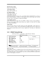
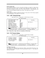
3-6-1 DRAM Timing Settings
CMOS Setup Utility – Copyright(C) 1984-2004 Award Software
DRAM Timing Settings
Item Help
System performance Manual
RAS Active Time 6T
RAS Precharge Time 3T
RAS to CAS Delay 3T
CAS Latency 2.5T
Bank Interleave 4 Bank
DRAM Burst Length 4
DRAM Command Rate 2T Command
Write Recovery Time 3T
Menu Level >>
↑↓→←
Move Enter:/-/PU/PD:Value F10:Save ESC:Exit F1:General Help
F5:Previous Values F6:Optimized Defaults F7:Standard Defaults
RAS Active Time
This field let’s you insert a timing delay between the CAS and RAS strobe signals, used when
DRAM is written to, read from, or refreshed.
Fast
gives faster performance; and
Slow
gives
more stable performance. This field applies only when synchronous DRAM is installed in the
system. The settings are: 2T and 3T.


