background image


Data Sheet: JN5142 

IEEE802.15.4 Wireless Microcontroller 


© NXP Laboratories UK 2012 

      JN-DS-JN5142 1v0 


Overview 


Features: Transceiver 


2.4GHz IEEE802.15.4 compliant 


128-bit AES security processor  


MAC accelerator with packet 
formatting, CRCs, address check, 
auto-acks, timers 


Integrated ultra low power  sleep 
oscillator 

– 0.5µA 


2.0V to 3.6V battery operation 


Deep sleep current 0.12µA 
(Wake-up from IO) 


0.5µA sleep with timer (1.5uA with 
RAM held) 


<$0.50 external component cost 


Rx current 16.5mA 


Tx current 14.8mA 


Receiver sensitivity -95dBm 


Transmit power 2.5dBm


Features: Microcontroller 


32-bit RISC CPU, 1 to 32MHz 
clock speed 


Low power operation 


Variable instruction width for high 
coding efficiency 


Multi-stage instruction pipeline 


128KB ROM and 32KB RAM for 
bootloaded program code 


RF4CE  or JenNet-IP software in 
ROM 


Master/Slave I2C interface.  


3xPWM and Application 
timer/counter 


UART 


SPI port with 3 selects 


Supply Voltage Monitor with 8 
programmable thresholds 


2- to 4-input 8-bit ADC, 
comparator 


Battery and temperature sensors 


Watchdog timer and Power-on-
Reset (with brown-out) circuit 


Up to 18 DIO 


Industrial temp -40°C to +125°C 
6x6mm 40-lead Punched QFN 

Lead-free and RoHS compliant 

The  JN5142  is  an  ultra  low  power,  high  performance  wireless 
microcontroller suitable for Remote Control, IEEE802.15.4 and Active RFID 
applications.  There  is  also  a  ROM  variant  that  supports  JenNet-IP  Smart 
Devices. The JN5142 features an enhanced 32-bit RISC processor offering 
high  coding  efficiency  through  variable  width  instructions,  a  multi-stage 
instruction  pipeline  and  low  power  operation  with  programmable  clock 
speeds.  It  also  includes  a  2.4GHz  IEEE802.15.4  compliant  transceiver, 
128KB of ROM, 32KB of RAM, and a comprehensive mix of analogue and 
digital peripherals. The operating current is below 18mA, allowing operation 
direct from a coin cell. 

The peripherals support a wide range of applications. They include a 2-wire 
serial  interface,  which  operates  as  either  master  or  slave,  a  two  channel 
ADC with battery and temperature sensors. A large switch matrix of up to 81 
elements  can  be  supported  for  remote  control  applications.  The  best  in 
class radio current and a 0.5µA sleep timer give excellent battery life. 

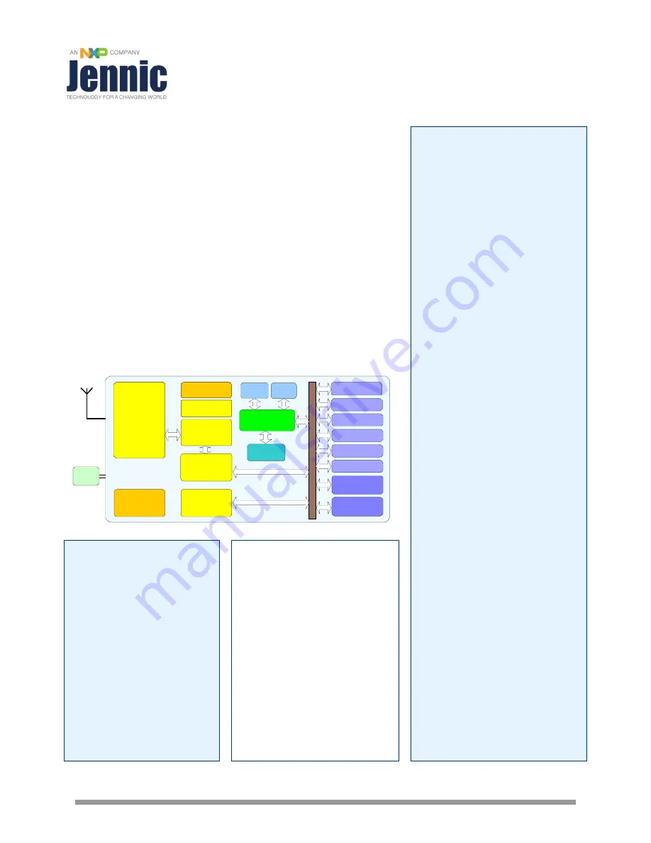
Block Diagram 

32-bit

RISC CPU

Timer

UART

4-Chan 8-bit

ADC

Battery and,

Temp Sensors

2-Wire Serial

(Master)

SPI

128-bit AES

Encryption
Accelerator

2.4GH

z

Radio

2.4GHz

Radio

ROM

128KB

Power

Management

XTAL

O-QPSK

Modem

29-byte

OTP eFuse

2-Wire Serial

(Slave)

Sleep Counter

Watchdog

Timer

Watchdog

Timer

Voltage Supply

Monitor

RAM

32KB

IEEE802.15.4

MAC

Accelerator


Benefits 


Single chip optimized for 
simple applications 


Very low current solution for 
long battery life 

– over 10 yrs 


RF4CE in ROM 


Variant for JenNet-IP Smart 
Devices 


Highly featured 32-bit RISC 
CPU for high performance 
and low power 


System BOM is low in 
component count and cost 


Flexible sensor interfacing 
options


Applications 


Robust and secure low power 
wireless applications using 
RF4CE 


Remote Control 


Toys and gaming peripherals 


Active RFID tags 


Point-to-point or star networks 
using IEEE802.15.4 


Energy harvesting, for example 
self powered light switch


Smart Lighting Networks


Building Automation


Summary of Contents for JN5142

Page 1: ...hrough variable width instructions a multi stage instruction pipeline and low power operation with programmable clock speeds It also includes a 2 4GHz IEEE802 15 4 compliant transceiver 128KB of ROM 32KB of RAM and a comprehensive mix of analogue and digital peripherals The operating current is below 18mA allowing operation direct from a coin cell The peripherals support a wide range of applicatio...

Page 2: ...ternal Memory 17 4 4 1 External Memory Encryption 18 4 5 Peripherals 18 4 6 Unused Memory Addresses 18 5 System Clocks 19 5 1 16MHz System Clock 19 5 1 1 32MHz Oscillator 19 5 1 2 High Speed RC Oscillator 20 5 2 32kHz System Clock 20 5 2 1 32kHz RC Oscillator 20 5 2 2 32kHz Crystal Oscillator 20 5 2 3 32kHz External Clock 21 6 Reset 22 6 1 Internal Brown out Reset 22 6 2 External Reset 23 6 3 Soft...

Page 3: ... 40 11 1 4 Delta Sigma Mode 40 11 1 5 Example Timer Counter Application 41 11 2 Tick Timer 41 11 3 Wakeup Timers 42 11 3 1 RC Oscillator Calibration 43 12 Pulse Counters 44 13 Serial Communications 45 13 1 Interrupts 46 13 2 UART Application 46 14 JTAG Debug Interface 48 15 Two Wire Serial Interface I2 C 49 15 1 Connecting Devices 49 15 2 Clock Stretching 50 15 3 Master Two wire Serial Interface 5...

Page 4: ...kHz Crystal Oscillator 67 19 3 10 32MHz Crystal Oscillator 67 19 3 11 High Speed RC Oscillator 68 19 3 12 Temperature Sensor 68 19 3 13 Radio Transceiver 69 Appendix A Mechanical and Ordering Information 75 A 1 SOT618 1 HVQFN40 40 pin QFN Package Drawing 75 A 2 Footprint information 76 A 3 Ordering Information 78 A 4 Device Package Marking 79 A 5 Tape and Reel Information 80 A 5 1 Tape Orientation...

Page 5: ... NXP Laboratories UK 2012 JN DS JN5142 1v0 5 Related Documents 93 RoHS Compliance 93 Status Information 93 Disclaimers 94 Version Control 94 Contact Details 95 ...

Page 6: ...ess Transceiver The Wireless Transceiver comprises a 2 45GHz radio a modem a baseband controller and a security coprocessor In addition the radio also provides an output to control transmit receive switching of external devices such as power amplifiers allowing applications that require increased transmit power to be realised very easily Appendix B 4 describes a complete reference design including...

Page 7: ...nterface compatible with SMbus and I 2 C supporting master and slave operation Eighteen digital I O lines multiplexed with peripherals such as timers and UARTs 8 bit Analogue to Digital converter with up to four input channels Programmable analogue comparator Internal temperature sensor and battery monitor Two low power pulse counters Random number generator Watchdog Timer and Supply Voltage Monit...

Page 8: ...AL_OUT Clock Divider Multiplier High speed RC Osc Watchdog Timer Voltage Supply Monitor Reset Wakeup Timer1 Wakeup Timer0 RESETN 32kHz Clock Select 32KIN Comparator1 COMP1P COMP1M ADC M U X ADC4 ADC1 VREF ADC2 ADC3 Temperature Sensor Supply Monitor 32kHz RC Osc 32kHz Clock Gen 32KXTALIN 32KXTALOUT PWMs Multiplexed with DIO pins PWM1 PWM3 PWM2 DIO6 TXD0 JTAG_TDO PWM2 DIO7 RXD0 JTAG_TDI PWM3 DIO4 CT...

Page 9: ...CK_GT DIO3 RFTX TIM0CAP SPICLK VSS1 SPIMISO SPIMOSI SPISELO VB_RAM DIO4 CTS0 TIM0OUT DIO5 RTS0 PWM1 PC1 DIO6 TXD0 PWM2 DIO7 RXD0 PWM3 VDD2 DIO15 SIF_D RXD0 SPISEL2 VSS2 DIO14 SIF_CLK TXD0 SPISEL1 DIO13 ADE PWM3 RTS0 DIO12 ADO PWM2 CTS0 VB_DIG DIO11 PWM1 DIO10 TIM0OUT 32KXTALOUT DIO9 TIM0CAP 32KXTALIN 32KIN DIO8 TIM0CK_GT PC1 Note JTAG occupies UART0 pins in either position Figure 2 40 pin QFN Conf...

Page 10: ...e Out Input 23 SPIMOSI CMOS SPI Master Out Slave In Output 24 SPISEL0 CMOS SPI Slave Select Output 0 16 DIO0 SPISEL1 ADC3 CMOS DIO0 SPI Slave Select Output 1 or ADC input 3 17 DIO1 SPISEL2 ADC4 PC0 CMOS DIO1 SPI Slave Select Output 2 ADC input 4 or Pulse Counter 0 Input 18 DIO2 TIM0CK_GT RFRX CMOS DIO2 Timer0 Clock Gate Input or Radio Receive Control Output 19 DIO3 TIM0CAP RFTX CMOS DIO3 Timer0 Ca...

Page 11: ...G_TDO SPISEL1 CMOS DIO14 Serial Interface Clock UART 0 Transmit Data Output JTAG Data Output or SPI Slave Select Output 1 40 DIO15 SIF_D RXD0 JTAG_TDI SPISEL2 CMOS DIO15 Serial Interface Data UART 0 Receive Data Input JTAG Data Input or SPI Slave Select Output 2 1 DIO16 COMP1P SIF_CLK CMOS DIO16 Comparator Positive Input or Serial Interface clock 2 DIO17 COMP1M SIF_D CMOS DIO17 Comparator Negative...

Page 12: ...iagram VSSA VSS1 VSS2 are the ground pins Users are strongly discouraged from connecting their own circuits to the 1 8v regulated supply pins as the regulators have been optimised to supply only enough current for the internal circuits 2 2 2 Reset RESETN is an active low reset input pin that is connected to a 300kΩ internal pull up resistor It may be pulled low by an external circuit Refer to Sect...

Page 13: ... COMP1P and COMP1M In reset sleep and deep sleep the analogue peripherals are all off In sleep the comparator may optionally be used as a wakeup source Unused ADC and comparator inputs should not be left unconnected for example connected to analogue ground VDD1 Analogue I O Pin VSSA Analogue Peripheral Figure 3 Analogue I O Cell 2 2 6 Digital Input Output Most digital I O pins on the JN5142 can ha...

Page 14: ... In reset the digital peripherals are all off and the DIO pins are set as high impedance inputs During sleep and deep sleep the DIO pins retain both their input output state and output level that was set as sleep commences If the DIO pins were enabled as inputs and the interrupts were enabled then these pins may be used to wake up the JN5142 from sleep ...

Page 15: ...data structures is very efficient due to the provision of several addressing modes together with the ability to be able to use any of the GP registers to contain the address of objects Subroutine parameter passing is also made more efficient by using GP registers rather than pushing objects onto the stack The recommended programming method for the JN5142 is by using C which is supported by a softw...

Page 16: ... single CPU clock cycle The ROM contents include bootloader to allow external Flash memory contents to be bootloaded into RAM at runtime a default interrupt vector table an interrupt manager IEEE802 15 4 MAC and APIs for interfacing on chip peripherals The operation of the boot loader is described in detail in Application Note 9 The interrupt manager routes interrupt calls to the application s sof...

Page 17: ...red in the external memory and a 128 bit AES security key A limited number of bits are available for customer use for storage of configuration information configuration of these is made through use of software APIs For further information on how to program and use the eFuse memory please contact technical support via the on line tech support system Alternatively NXP can provide an eFuse programmin...

Page 18: ...rocessor combined with a user programmable 128 bit encryption key is used to encrypt the contents of the external memory The encryption key is stored in eFuse When bootloading program code from external serial memory the JN5142 automatically accesses the encryption key to execute the decryption process User program code does not need to handle any of the decryption process it is transparent With e...

Page 19: ... known On wake up from sleep the JN5142 uses the Fast RC oscillator It can then either Automatically switch over to use the 32MHz clock source when it has started up Continue to use the fast RC oscillator until software triggers the switch over to the 32MHz clock source for example when the radio is required Continue to use the RC oscillator until the device goes back into one of the sleep modes C...

Page 20: ... useful as a timing source for accurate wakeup from sleep a frequency calibration factor derived from the more accurate 16MHz clock may be applied The calibration factor is derived through software details can be found in Section 11 3 1 Software must check that the 32kHz RC oscillator is running before using it For detailed electrical specifications see Section 19 3 8 5 2 2 32kHz Crystal Oscillato...

Page 21: ...Hz reference clock on the 32KIN input DIO9 may be provided to the JN5142 This would allow the 32kHz system clock to be sourced from a very stable external oscillator module allowing more accurate sleep cycle timings compared to the internal RC oscillator See Section 19 2 3 DIO9 is a 3V tolerant input ...

Page 22: ...imer Supply Voltage detect Note When the device exits a reset condition device operating parameters voltage frequency temperature etc must be met to ensure operation If these conditions are not met then the device must be held in reset until the operating conditions are met See Section 19 3 6 1 Internal Power On Brown out Reset BOR For the majority of applications the internal power on reset is ca...

Page 23: ...m reset can be triggered at any time through software control causing a full chip reset and invalidating the RAM contents For example this can be executed within a user s application upon detection of a system failure 6 4 Supply Voltage Monitor SVM An internal Supply Voltage Monitor SVM is used to monitor the supply voltage to the JN5142 this can be used whilst the device is awake or is in CPU doz...

Page 24: ...re configured timer period will cause a chip reset to be performed A status bit is set if the watchdog was triggered so that the software can differentiate watchdog initiated resets from other resets and can perform any required recovery once it restarts After power up reset start from deep sleep or start from sleep the watchdog is always enabled with the largest timeout period and will commence c...

Page 25: ... Stack overflow Table 2 Interrupt Vectors 7 1 System Calls The b trap and b sys instructions allow processor exceptions to be generated by software A system call exception will be generated when the b sys instruction is executed This exception can for example be used to enable a task to switch the processor into supervisor mode when a real time operating system is in use See Section 3 for further ...

Page 26: ...xternal interrupt handling i e interrupts from hardware peripherals is provided to enable an application to control an events priority to provide for deterministic program execution The priority Interrupt controller provides 15 levels of prioritised interrupts The priority level of all interrupts can be set with value 0 being used to indicate that the source can never produce an external interrupt...

Page 27: ...r VCO The VCO has no external components and includes calibration circuitry to compensate for differences in internal component values due to process and temperature variations The VCO is controlled by a Phase Locked Loop PLL that has an internal loop filter A programmable charge pump is also used to tune the loop characteristic The receiver chain starts with the low noise amplifier mixer combinat...

Page 28: ...ed to present an accurate match to a 50 ohm resistive network as well as provide a DC path to the final output stage or antenna Users wishing to match to other active devices such as amplifiers should design their networks to match to 50 ohms at the output of L1 R1 43K IBIAS C20 100nF L2 2 7nH VB_RF VREF VB_RF2 RF_IN C3 100nF C12 47pF VB_RF1 C1 47pF L1 5 6nH To Coaxial Socket or Integrated Antenna...

Page 29: ...gure 16 Simple Antenna Diversity Implementation using External RF Switch ADO DIO 12 TX Active RX Active ADE DIO 13 1st TX RX Cycle 2nd TX RX Cycle 1st Retry Figure 17 Antenna Diversity ADO Signal for TX with Acknowledgement If two DIO pins cannot be spared DIO13 can be configured to be a normal DIO pin and the inverse of ADO generated with an inverter on the PCB ...

Page 30: ...s include Energy Detection ED Link Quality Indication LQI and fully programmable Clear Channel Assessment CCA The Modem provides a digital Receive Signal Strength Indication RSSI that facilitates the implementation of the IEEE 802 15 4 ED function and LQI function The ED and LQI are both related to receiver power in the same way as shown in Figure 19 LQI is associated with a received packet wherea...

Page 31: ...as superframe timing and slot boundaries Once the packet is prepared and protocol timer set the supervisor block controls the transmission When the scheduled time arrives the supervisor controls the sequencing of the radio and modem to perform the type of transmission required It can perform all the algorithms required by IEEE802 15 4 such as CSMA CA without processor intervention including retrie...

Page 32: ...chedules the beacons and transmits them without CPU intervention 8 3 5 Security The transmission and reception of secured frames using the Advanced Encryption Standard AES algorithm is handled by the security coprocessor and the stack software The application software must provide the appropriate encrypt decrypt keys for the transmission or reception On transmission the key can be programmed at th...

Page 33: ...e device is sleeping these interrupts become events that can be used to wake the device up Equally the status of the interrupt may be read See Section 18 for further details on sleep and wakeup The state of all DIO pins can be read irrespective of whether the DIO is configured as an input or an output Throughout a sleep cycle the direction of the DIO and the state of the outputs is held This is ba...

Page 34: ...C3 DIO3 RFTX TIM0CAP DIO2 RFRX TIM0CK_GT DIO1 SPISEL2 PC0 ADC4 DIO9 TIM0CAP 32KXTALIN DIO8 TIM0CK_GT PC1 DIO13 PWM3 ADE RTS0 JTAG_TMS DIO11 PWM1 DIO12 PWM2 ADO CTS0 JTAG_TCK DIO14 SIF_CLK TXD0 JTAG_TD0 SPISEL1 DIO15 SIF_D RXD0 JTAG_TDI SPISEL2 DIO16 COMP1P SIF_CLK SPISEL1 SPISEL2 TXD0 RXD0 RTS0 CTS0 TIM0CK_GT TIM0CAP TIM0OUT SIF_D SIF_CLK Pulse Counters PC0 PC1 JTAG Debug JTAG_TDI JTAG_TMS JTAG_TC...

Page 35: ...it and receive data simultaneously There are three dedicated pins SPICLK SPIMOSI SPIMISO that are shared across all devices on the bus Master Out Slave In or Master In Slave Out data transfer is relative to the clock signal SPICLK generated by the JN5142 The JN5142 provides three slave selects SPISEL0 to SPISEL2 to allow three SPI peripherals on the bus SPISEL0 is a dedicated pin this is generally...

Page 36: ... Valid data is output on SPIMOSI before the first clock edge and is changed every positive edge SPIMISO is sampled every negative edge 1 1 3 SPICLK is high when idle the first edge is negative Valid data is output on SPIMOSI every negative edge SPIMISO is sampled every positive edge Table 4 SPI Configurations If more than one SPISEL line is to be used in a system they must be used in numerical ord...

Page 37: ...y separate SPI accesses and therefore manual slave select mode must be used The required slave select can then be asserted active low at the start of the transfer A sequence 8 and 32 bit transfers can be used to issue the command and address to the FLASH device and then to read data back Finally the slave select can be deselected to end the transaction 0 1 2 3 4 5 6 7 Instruction 0x03 23 22 21 3 2...

Page 38: ...w or both transitions PWM Single pulse outputs repeating Pulse Width Modulation signal or a single pulse Can set period and mark space ratio Capture measures times between transitions of an applied signal Delta Sigma Return To Zero RTZ and Non Return to Zero NRZ modes Timer usage of external IO can be controlled on a pin by pin basis Three further timers are also available that support the same fu...

Page 39: ...lation Mode Pulse Width Modulation PWM mode as used by PWM timers 1 2 and 3 and optionally by Timer0 allows the user to specify an overall cycle time and pulse length within the cycle The pulse can be generated either as a single shot or as a train of pulses with a repetition rate determined by the cycle time In this mode the cycle time and low periods of the PWM output signal can be set by the va...

Page 40: ...ream of pulses with digital voltage levels is generated which is integrated by the RC network to give an analogue voltage A conversion time is defined in terms of a number of clock cycles The width of the pulses generated is the period of a clock cycle The number of pulses output in the cycle together with the integrator RC values will determine the resulting analogue voltage For example generatin...

Page 41: ... a constant period This converts the tacho pulse stream output into a count proportional to the motor speed This value is then used by the application software executing the control algorithm If required for other functionality then the unused IO associated with the timers could be used as general purpose DIO JN5142 PWM1 Timer0 CLK GATE CAPTURE PWM M Tacho 1N4007 12V IRF521 1 pulse rev Figure 31 C...

Page 42: ...ogrammed as restartable the operation of the counter is the same as for the single shot mode except that when the match value is reached the counter is reset and begins counting from zero An interrupt will be generated when the match value is reached if it is enabled Continuous mode operation is similar to restartable except that when the match value is reached the counter is not reset but continu...

Page 43: ...programmed to wake up very close to the calculated time of the event and so keep current consumption to a minimum If the sleep time is less accurate it will be necessary to wake up earlier in order to be certain the event will be captured If the device wakes earlier it will be awake for longer and so reduce battery life In order to allow sleep time periods to be as close to the desired length as p...

Page 44: ... 16 bit reference that is loaded by the user An interrupt and wakeup event if asleep may be generated when a counter reaches its pre configured reference value The two counters may optionally be cascaded together to provide a single 32 bit counter linked to DIO1 The counters do not saturate at 65535 but naturally roll over to 0 Additionally the pulse counting continues when the reference value is ...

Page 45: ...n Flow control by software or automatically by hardware Processor Bus Divisor Latch Registers Line Status Register Line Control Register FIFO Control Register Receiver FIFO Transmitter FIFO Baud Generator Logic Transmitter Shift Register Receiver Shift Register Transmitter Logic Receiver Logic RXD TXD Modem Control Register Modem Status Register Modem Signals Logic RTS CTS Interrupt ID Register In...

Page 46: ...r purposes Note With the automatic flow control threshold set to 15 the hardware flow control within the UART block negates RTS when the receive FIFO is about to become full In some instances it has been observed that remote devices that are transmitting data do not respond quickly enough to the de asserted CTS and continue to transmit data In these instances the data will be lost in a receive FIF...

Page 47: ...oratories UK 2012 JN DS JN5142 1v0 47 JN5142 RTS CTS TXD RXD UART0 RS232 Level Shifter 1 2 3 4 5 6 7 8 9 CD RD TD DTR SG DSR RTS CTS RI PC COM Port Pin Signal 1 5 6 9 Figure 34 JN5142 Serial Communication Link ...

Page 48: ...s dealt with in 4 The following table details which DIO are used for the JTAG interface depending upon the configuration Signal DIO Assignment Standard pins Alternative pins clock TCK 26 36 control TMS 27 37 data out TDO 28 38 data in TDI 29 40 Table 7 Hardware Debugger IO If doze mode is active when debugging is started the processor will be woken and then respond to debugger commands It is not p...

Page 49: ...knowledge mechanism Read data preloaded or provided as required The Serial Interface is accessed depending upon the configuration DIO14 and DIO15 or DIO16 and DIO17 This is enabled under software control The following table details which DIO are used for the Serial Interface depending upon the configuration Signal DIO Assignment Standard pins Alternative pins SIF_CLK 38 1 SIF_D 40 2 Table 8 Two Wi...

Page 50: ...t across the two wire interface when indicated and read data received on the interface is made available in a receive buffer Indication of when a particular transfer has completed may be indicated by means of an interrupt or by polling a status bit The first byte of data transferred by the device after a start bit is the slave address The JN5142 supports both 7 bit and 10 bit slave addresses by ge...

Page 51: ... State Figure 37 Multi Master Clock Synchronisation After each transfer has completed the status of the device must be checked to ensure that the data has been acknowledged correctly and that there has been no loss of arbitration N B Loss of arbitration may occur at any point during the transfer including data cycles An interrupt will be generated when arbitration has been lost ...

Page 52: ... receive buffer by the processor before the next byte of data arrives To enable this the interface may be configured to work in two possible backoff modes Not Acknowledge mode where the interface returns a Not Acknowledge NACK to the master if more data is received before the previous data has been taken This will lead to the termination of the current data transfer Clock Stretching mode where the...

Page 53: ...oximately 0 25msec to complete Alternatively continuous generation mode can be used where a new number is generated approximately every 0 25msec In either mode of operation an interrupt can be generated to indicate when the number is available or a status bit can be polled The random bits are generated by sampling the state of the 32MHz clock every 32kHz system clock edge As these clocks are async...

Page 54: ...nput 2 cannot be used if an external reference is required as this uses the same pin as VREF Note also that ADC3 and ADC4 use the same pins as DIO0 SPISEL1 and DIO1 SPISEL2 respectively These pins can only be used for the ADC if they are not required for their alternative functions Similarly the comparator inputs are shared with DIO16 SIF_CLK and DIO17 SIF_D If used for their analogue functions th...

Page 55: ...tance of the switches and the sampling capacitor 8pF The sampling time required can then be calculated by adding the sensor source resistance to the switch resistance multiplying by the capacitance giving a time constant Assuming normal exponential RC charging the number of time constants required to give an acceptable error can be calculated 6 time constants gives an error of 0 25 so for 8 bit ac...

Page 56: ...e out of sleep mode the user application should wait until the temperature has stabilised before taking a measurement 17 2 Comparator The JN5142 contains one analogue comparator COMP1 that is designed to have true rail to rail inputs and operate over the full voltage range of the analogue supply VDD1 The hysteresis level can be set to a nominal value of 0mV 10mV 20mV or 40mV The source of the nega...

Page 57: ...ures for the different modes of operation of the device is given in Section 19 2 2 18 2 Active Processing Mode Active processing mode in the JN5142 is where all of the application processing takes place By default the CPU will execute at the selected clock speed executing application firmware All of the peripherals are available to the application as are options to actively enable or disable them ...

Page 58: ...hese timers are described in Section 11 3 Timer events can be generated from both of the two timers one is intended for use by the 802 15 4 protocol the other being available for use by the Application running on the CPU These timers are available to run at any time even during sleep mode 18 3 2 DIO Event Any DIO pin when used as an input has the capability by detecting a transition to generate a ...

Page 59: ...low soldering temperature according to IPC JEDEC J STD 020C 260ºC ESD rating Human Body Model 1 2 0kV Charged Device Model 2 Exception XTALOUT 350V 500V 1 Testing for Human Body Model discharge is performed as specified in JEDEC Standard JESD22 A114 2 Testing for Charged Device Model discharge is performed as specified in JEDEC Standard JESD22 C101 19 2 DC Electrical Characteristics 19 2 1 Operati...

Page 60: ...or 73 0 8 µA Normal low power UART 90 µA For each UART Timer 30 µA For each Timer 2 wire serial interface I2 C 70 µA 19 2 2 2 Sleep Mode Mode Min Typ Max Unit Notes Sleep mode with I O wakeup 0 12 µA Waiting on I O event Sleep mode with I O and RC Oscillator timer wakeup measured at 25ºC 0 73 µA As above but also waiting on timer event If both wakeup timers are enabled then add another 0 05µA 32kH...

Page 61: ...Digital I O low Input 0 3 VDD2 x 0 27 V Digital I O input hysteresis 140 230 310 mV DIO High O P 2 7 3 6V VDD2 x 0 8 VDD2 V With 4mA load DIO Low O P 2 7 3 6V 0 0 4 V With 4mA load DIO High O P 2 2 2 7V VDD2 x 0 8 VDD2 V With 3mA load DIO Low O P 2 2 2 7V 0 0 4 V With 3mA load DIO High O P 2 0 2 2V VDD2 x 0 8 VDD2 V With 2 5mA load DIO Low O P 2 0 2 2V 0 0 4 V With 2 5mA load Current sink source c...

Page 62: ...threshold voltage VPOT Rise fall time 10mS 1 47 1 42 V Rising Falling Spike Rejection Square wave pulse 1us Triangular wave pulse 10us 1 2 1 3 V Depth of pulse to trigger reset Reset stabilisation time tSTAB 45 µs Note 1 Supply Voltage Monitor Threshold Voltage VTH 1 88 1 92 2 03 2 12 2 22 2 31 2 60 2 89 1 96 2 00 2 11 2 21 2 31 2 41 2 71 3 01 2 02 2 06 2 17 2 28 2 38 2 48 2 79 3 10 V Configurable...

Page 63: ... 1 3 SS MOSI mode 0 2 MISO mode 0 2 MISO mode 1 3 tVO tVO CLK mode 0 1 tSI tHI CLK mode 2 3 Figure 43 SPI Timing Master Parameter Symbol Min Max Unit Clock period tCK 62 5 ns Data setup time tSI 16 7 3 3V 18 2 2 7V 21 0 2 0V ns Data hold time tHI 0 ns Data invalid period tVO 15 ns Select set up period tSSS 60 ns Select hold period tSSH 30 SPICLK 16MHz 0 SPICLK 16MHz mode 0 or 2 60 SPICLK 16MHz mod...

Page 64: ...e time between a STOP and START condition tBUF 4 7 1 3 µs Pulse width of spikes that will be suppressed by input filters Note 1 tSP 60 60 ns Capacitive load for each bus line Cb 400 400 pF Noise margin at the LOW level for each connected device including hysteresis Vnl 0 1VDD 0 1VDD V Noise margin at the HIGH level for each connected device including hysteresis Vnh 0 2VDD 0 2VDD V Note 1 This figu...

Page 65: ...in Typ Max Unit Notes Resolution 8 bits 500kHz Clock Current consumption 655 µA Integral nonlinearity 1 1 2 LSB Differential nonlinearity 0 5 0 5 LSB Guaranteed monotonic Offset error 10 20 mV 0 to Vref range 0 to 2Vref range Gain error 10 20 mV 0 to Vref range 0 to 2Vref range Internal clock 0 25 0 5 or 1 0 MHz 16MHz input clock 16 32or 64 No internal clock periods to sample input 2 4 6 or 8 Prog...

Page 66: ...12 28 10 20 40 16 17 26 29 50 55 mV Programmable in 3 steps and zero Vref Internal See Section 19 3 5 V Common Mode input range 0 Vdd V Current normal mode 54 73 102 110 µA Current low power mode 0 8 1 1 1 2 µA 19 3 8 32kHz RC Oscillator VDD 2 0 to 3 6V 40 to 125 ºC italic 85 ºC Bold 125 ºC Parameter Min Typ Max Unit Notes Current consumption of cell and counter logic 680 600 500 830 930 750 850 6...

Page 67: ...ance needs to be 2 CL allowing for stray capacitance from chip package and PCB Amplitude at Xout Vdd 0 2 Vp p 19 3 10 32MHz Crystal Oscillator VDD 2 0 to 3 6V 40 to 125ºC italic 85 ºC Bold 125 ºC Parameter Min Typ Max Unit Notes Current consumption 300 375 450 500 µA Excluding bandgap ref Start up time 0 74 ms Assuming xtal with ESR of less than 40ohms and CL 9pF External caps 15pF see Appendix B ...

Page 68: ...tion with temperature 0 035 0 025 0 015 0 010 C Variation with VDD2 0 65 0 35 0 2 0 1 V Startup time 2 4 us 19 3 12 Temperature Sensor VDD 2 0 to 3 6V 40 to 125ºC italic 85 ºC Bold 125 ºC Parameter Min Typ Max Unit Notes Operating Range 40 125 C Sensor Gain 1 44 1 55 1 66 mV C Accuracy 10 C Non linearity 2 5 3 5 C Output Voltage 630 570 855 mV Includes absolute variation due to manufacturing temp ...

Page 69: ...CC part 15 rules IC Canada ETSI ETS 300 328 and Japan ARIB STD T66 The PCB schematic and layout rules detailed in Appendix B 4 must be followed Failure to do so will likely result in the JN5142 failing to meet the performance specification detailed herein and worst case may result in device not functioning in the end application Parameter Min Typical Max Notes RF Port Characteristics Type Single E...

Page 70: ...bove sensitivity Note1 Out of band rejection 52 dBc For 1 PER with wanted signal 3dB above sensitivity All frequencies except wanted 2 which is 8dB lower Note1 Spurious emissions RX 61 70 58 dBm Measured conducted into 50ohms 30MHz to 1GHz 1GHz to 12GHz Intermodulation protection 40 dB For 1 PER at with wanted signal 3dB above sensitivity Modulated Interferers at 2 4 channel separation Note1 RSSI ...

Page 71: ...bove sensitivity Note1 Out of band rejection 49 dBc For 1 PER with wanted signal 3dB above sensitivity All frequencies except wanted 2 which is 8dB lower Note1 Spurious emissions RX 60 70 57 dBm Measured conducted into 50ohms 30MHz to 1GHz 1GHz to 12GHz Intermodulation protection 39 dB For 1 PER at with wanted signal 3dB above sensitivity Modulated Interferers at 2 4 channel separation Note1 RSSI ...

Page 72: ...e sensitivity Note1 Out of band rejection 53 dBc For 1 PER with wanted signal 3dB above sensitivity All frequencies except wanted 2 which is 8dB lower Note1 Spurious emissions RX 62 70 59 dBm Measured conducted into 50ohms 30MHz to 1GHz 1GHz to 12GHz Intermodulation protection 41 dB For 1 PER at with wanted signal 3dB above sensitivity Modulated Interferers at 2 4 channel separation Note1 RSSI lin...

Page 73: ...ve sensitivity Note1 Out of band rejection 53 dBc For 1 PER with wanted signal 3dB above sensitivity All frequencies except wanted 2 which is 8dB lower Note1 Spurious emissions RX 64 70 61 dBm Measured conducted into 50ohms 30MHz to 1GHz 1GHz to 12GHz Intermodulation protection 41 dB For 1 PER at with wanted signal 3dB above sensitivity Modulated Interferers at 2 4 channel separation Note1 RSSI li...

Page 74: ...Blocker rejection is defined as the value when 1 PER is seen with the wanted signal 3dB above sensitivity as per 802 15 4 Section 6 5 3 4 Note2 Channels 11 17 24 low high values reversed Note3 Up to an extra 2 5dB of attenuation is available if required ...

Page 75: ...0 pin QFN Package Drawing Figure 45 40 pin QFN Package Drawings UNIT A max A1 b c D Dh E Eh e e1 e2 L v w y y1 mm 1 0 05 0 00 0 30 0 18 0 2 6 1 5 9 4 75 4 45 6 1 5 9 4 75 4 45 0 5 4 5 4 5 0 5 0 3 0 1 0 05 0 05 0 1 Table 11 Package Dimensions Plastic or metal protrusions of 0 075 mm maximum per side are not included ...

Page 76: ... for reflow soldering All dimensions are given in the table underneath Figure 46 PCB Decal P Ax Ay Bx By C D SLx Sly SPx tot Spy tot SPx Spy Gx Gy Hx Hy 0 500 7 000 7 000 5 200 5 200 0 900 0 290 4 100 4 100 2 400 2 400 0 600 0 600 6 300 6 300 7 250 7 250 Table 12 Footprint Dimensions ...

Page 77: ...schematic and layout rules detailed in Appendix B 4 must be followed Failure to do so will likely result in the JN5142 failing to meet the performance specification detailed herein and worst case may result in device not functioning in the end application ...

Page 78: ...ces on a 180mm reel Order Codes Part Number Ordering Code Description JN5142 001 JN5142N 001 JN5142 microcontroller with 001 ROM JN5142 J01 JN5142N J01 JN5142 microcontroller with J01 ROM The Standard Supply Multiple SSM for Engineering Samples or Prototypes is 50 units with a maximum of 250 units If the quantity of Engineering Samples or Prototypes ordered is less than a reel quantity then these ...

Page 79: ... a JN5142 device with revision B ROM software that came from assembly build number 01 and was manufactured week 25 of 2011 JN5142S XXXXXX XXXXFF XXXYWWXX JN5142B RUL280 00YU01 qSD125 X NXP NXP Figure 47 Device Package Marking Legend JN Family part code XXXX 4 digit part number S Software ROM identifier letter FF 2 digit assembly build number Y 1 digit year number WW 2 digit week number Network Sta...

Page 80: ...Figure 49 shows the detailed dimensions of the tape used for 6x6mm 40QFN devices Reference Dimensions mm Ao 6 30 0 10 Bo 6 30 0 10 Ko 1 10 0 10 F 7 500 0 10 P1 12 0 0 10 W 16 00 0 30 0 3 I Measured from centreline of sprocket hole to centreline of pocket II Cumulative tolerance of 10 sprocket holes is 0 20mm III Measured from centreline of sprocket hole to centreline of pocket IV Other material av...

Page 81: ... 1x10 10 1x10 12 Ohms Square Material High Impact Polystyrene environmentally friendly recyclable All dimensions and tolerances are fully compliant with EIA 481 B and are specified in millimetres 6 window design with one window on each side blanked to allow adequate labelling space Figure 50 Reel Dimensions ...

Page 82: ... space Figure 51 330mm Reel Dimensions A 5 4 Dry Pack Requirement for Moisture Sensitive Material Moisture sensitive material as classified by JEDEC standard J STD 033 must be dry packed The 56 lead QFN package is MSL2A 260 C and is dried before sealing in a moisture barrier bag MBB with desiccant bag weighing at 67 5 grams of activated clay and a humidity indicator card HIC meeting MIL L 8835 spe...

Page 83: ...ins from all sources As the load capacitance CL affects the oscillation frequency by a process known as pulling crystal manufacturers specify the frequency for a given load capacitance only A typical pulling coefficient is 15ppm pF to put this into context the maximum frequency error in the IEEE802 15 4 specification is 40ppm for the transmitted signal Therefore it is important for resonance at 32...

Page 84: ...fective crystal resistance This gives 2 2 1 T T m C C g 2 4 L L S m C C C R This can be used to give an equation for the required transconductance 2 1 2 2 1 2 1 2 4 T T T T T T S m m C C C C C C C R g Example Using typical 32MHz crystal parameters of m R 40 S C 1pF and 1 T C 2 T C 18pF for a load capacitance of 9pF the equation above gives the required transconductance m g as 2 59mA V The JN5142 h...

Page 85: ... being coupled into the oscillator XTALOUT C2 C1 R1 XTALIN JN5142 Figure 52 Crystal Oscillator Connections The clock generated by this oscillator provides the reference for most of the JN5142 subsystems including the transceiver processor memory and digital and analogue peripherals 32MHz Crystal Requirements Parameter Min Typ Max Notes Crystal Frequency 32MHz Crystal Tolerance 40ppm Including temp...

Page 86: ...ce of 9 or 10pF is widely available and the max ESR of 30 ohms specified by many manufacturers is acceptable Also available in this package style are crystals with a load capacitance of 12pF but in this case the max ESR required is 25 ohms or better Below is measurement data showing the variation of the crystal oscillator amplifier transconductance with temperature and supply voltage notice how sm...

Page 87: ... in 19 3 9 The oscillator cell is flexible and can operate with a range of commonly available 32kHz crystals with load capacitances from 6 to 12 5p and ESR up to 80K It achieves this by using automatic gain control AGC which senses the signal swing As explained in Appendix B 1 3 there is a trade off that exists between the load capacitance and crystal ESR to achieve reliable performance The use of...

Page 88: ...equation in Appendix B 1 2 Load Capacitance Ext Capacitors Current Start up Time Max ESR 9pF 15pF 1 6µA 0 8Sec 70K 6pF 9pF 1 4µA 0 6sec 80K 12 5pF 22pF 2 4µA 1 1sec 35K Below is measurement data showing the variation of the crystal oscillator supply current with voltage and with crystal ESR for two load capacitances 0 6 0 8 1 1 2 1 4 1 6 2 2 2 4 2 6 2 8 3 3 2 3 4 3 6 Normalised Current IDD Supply ...

Page 89: ...e tech support system www jennic com support B 4 1 Schematic Diagram A schematic diagram of the JN5142 PCB antenna reference module is shown in 1 40 39 38 37 36 35 34 33 32 31 VSSA 2 3 4 5 6 7 8 9 10 30 29 28 27 26 25 24 23 22 21 20 19 18 17 16 15 14 13 12 11 COMP1P COMP1M RESETN XTAL_OUT XTAL_IN VB_SYNTH VCOTUNE NC VB_VCO VDD1 IBIAS VREF VB_RF2 RF_IN VB_RF ADC1 SPISEL1 SPISEL2 DIO2 DIO3 SPICLK VS...

Page 90: ...MOSI SPISELO VB_RAM CTS0 RTS0 TXD0 RXD0 VDD2 SIF_D VSS2 SIF_CLK DIO13 DIO12 VB_DIG DIO11 TIM0OUT TIM0CAP TIM0CK_GT C7 100nF 2 wire Serial Port Timer0 C16 100nF UART0 JTAG C6 100nF Serial Flash Memory VDD SDO WP VSS SS VCC HOLD CLK SDI SPI Select Analogue IO C12 47pF C3 100nF C1 47pF L1 5 6nH L2 2 7nH VB_RF R1 43k To coaxial socket or integrated antenna C20 100nF C14 100nF C13 10µF VDD C2 10nF C15 ...

Page 91: ...1 pin 35 R1 43k I Bias Resistor Less than 5mm from U1 pin 10 C20 100nF Vref decoupling optional Less than 5mm from U1 pin 11 U2 1Mbit Serial Flash Memory Micron M25P10 Y1 32MHz Crystal AEL X32M000000S039 or Epson Toyocom X1E000021016700 CL 9pF Max ESR 40R C10 15pF 5 COG Crystal Load Capacitor Adjacent to pin 4 and Y1 pin 1 C11 15pF 5 COG Crystal Load Capacitor Adjacent to pin 5 and Y1 pin 3 C1 47p...

Page 92: ...ion information 7 which describes the reflow soldering process The suggested reflow profile from that application note is shown in Figure 55 The specific paste manufacturers guidelines on peak flow temperature soak times time above liquidus and ramp rates should also be referenced Figure 55 Recommended Reflow Profile for Lead free Solder Paste SNAgCu or PPF Lead Frame B 4 3 Moisture Sensitivity Le...

Page 93: ... Low Power RF products progress according to the following format Advance The Data Sheet shows the specification of a product in planning or in development The functionality and electrical performance specifications are target values of the design and may be used as a guide to the final specification Integrated circuits are identified with an Rx suffix for example JN5142R1 NXP reserves the right t...

Page 94: ...esentation or warranty that such applications will be suitable for the specified use without further testing or modification NXP Semiconductors assumes no responsibility or liability for the use of any of these products conveys no license or title under any patent copyright or mask work right to these products and makes no representations or warranties that these products are free from patent copy...

Page 95: ...1v0 95 Contact Details NXP Laboratories UK Ltd Furnival Street Sheffield S1 4QT United Kingdom Tel 44 0 114 281 2655 Fax 44 0 114 281 2951 For the contact details of your local NXP office or distributor refer to the NXP web site www nxp com ...

Reviews: