background image

30       Operation and Control Instructions

Operation and Control using the Simplex Parallel Interface (SK/SP Emulation  Mode)

The Simplex Parallel Interface (Emulation Mode)

The Simplex parallel interface is fully backwards compatible to the interface used on the SK/SP 
Series Fiberoptic switch.  It also provides a simple interface when the advanced features of the SKB 
are not required.

The interface permits channel numbers to be strobed in using the STROBE line.  As a reference for 
SK/SP users, the typical method of interface to a host controller for the SK/SP Series Fiberoptic 
Switch is shown below for reference.

Figure 9: Typical Controller Connections

Simultaneous operation of serial and parallel interface is not supported.

Simplex Parallel Interface:  Pin Functional Description

Data Lines (D0 to D6)

Valid channel numbers are strobed in through the data lines on high-to-low transitions of the /Strobe 
line. When a new channel is strobed in, the SK switch immediately selects the channel. The channel 

Summary of Contents for SKB Series

Page 1: ...SKB SERIES FIBEROPTIC SWITCH MODULE User Manual ...

Page 2: ...ii 10109002 Rev 001 August 2001 2001 JDS Uniphase All rights reserved ...

Page 3: ... com Website www jdsuniphase com Instrumentation and Controls Customer Support and Service Emergency technical support is available seven days a week 24 hours a day Telephone 1 613 727 1304 extension 4999 Global Toll Free Canada and U S 1 800 406 9559 All Other Countries International Access Code 800 406 95599 E mail instrumentsupport jdsuniphase com Refer to the JDSU Terms and Conditions of Sale ...

Page 4: ...iv ...

Page 5: ...rom the date of the shipment or in the case of services net thirty 30 days from the date of completion JDSU reserves the right to require alternative payment terms including without limitation letter of credit or payment in advance If at any time Customer is delinquent in the payment of any invoice or is otherwise in breach of this Agreement JDSU may at its discretion stop performance of services ...

Page 6: ...ense the use of the Software to any third party or c permit or authorize anyone within Customer s reasonable control to do any acts in a or b JDSU warrants that the Software under normal use and service as originally delivered to Customer will func tion substantially in accordance with the functional description set out in the Product specification and or user manual supplied with the Software for...

Page 7: ... of the State of New York and all courts competent to hear appeal there from 13 2 JDSU shall not be liable for any delay or failure in performance whatsoever due to acts of God earthquakes shortage of supplies transpor tation difficulties labor disputes riots war fire explosion epidemics or other occurrences beyond JDSU s reasonable control or due to unfore seen circumstances 13 3 Waiver by JDSU o...

Page 8: ...ng Time Between Channels 9 Getting Started 11 Before Initializing and Operating the Unit 11 Initial Inspection 11 Operating Environment 11 Temperature 11 Humidity 12 Storing and Shipping 12 Claims and Repackaging 12 Returning Shipments to JDS Uniphase 12 Cleaning Connectors 13 Storing Fiberoptic Connectors 14 Handling Fiberoptic Cables 14 Installation and Physical Interface 15 Overview of Physical...

Page 9: ...put Line 31 Busy Output Line 31 Error Output Line 31 Timing 32 Timing Key 32 Operation and Control using the Enhanced Parallel Interface 33 Enhanced Parallel Interface 33 Enhanced Parallel Interface Voltage Levels 33 Enhanced Parallel Timing 33 Enhanced Parallel Interface Line Descriptions 34 Data Lines D0 D7 34 SOP Input Line 34 STROBE Input Line 34 R W Input Line 34 BUSY Output Line 34 ERROR Out...

Page 10: ...omparison and Harness Wiring 88 APPLICATION NOTE Controlling An SKB Switch using a PC Printer Port 90 Setting the Computer to EPP Mode 90 Using the Printer Port 90 APPLICATION NOTE Custom SKB with D Subminiature Style connectors 91 Connector Description 92 The Power and Serial Interface Connector 93 The Parallel Interface 94 Service 97 Returning a Unit 97 Shipping a Unit 97 ...

Page 11: ...7 Contents ...

Page 12: ...on 29 Typical Controller Connections 30 Timing Diagram 32 Flowchart of Read Cycle 36 Flowchart of Write Cycle 37 SKB enhanced mode 5 byte write master to slave high speed 79 SKB enhanced mode 5 byte write master to slave low speed 80 Three byte response packet read from SKB high speed 81 Three byte response packet read from SKB low speed 82 SKB with SK SP Emulation Adaptor Harness 87 SKB to SK SP ...

Page 13: ...9 List of Figures ...

Page 14: ... Enhanced Parallel Interface on 25x2 IDE connector 20 Pin Assignment Power using the 4x1 Power Connector 22 Pin Assignment Power using the Power Pins on the 25x2 IDE Connector 22 Parameter Data Types 25 RS485 Addresses 27 RS485 Link Layer Packet Fields 28 Channel Address Table 31 Timing Key 32 Enhanced Parallel Interface States 33 SKB II to SK Adapter Harness Wiring 88 Cable Wiring for Printer Por...

Page 15: ...11 List of Tables ...

Page 16: ... Instructions The following safety instructions must be observed whenever the unit is operated serviced or repaired Failure to comply with any of these instructions or with any precaution or warning contained in the user s manual is in direct violation of the standards of design manufacture and intended use of the unit JDS Uniphase assumes no liability for the customer s failure to comply with any...

Page 17: ...le and direct exposure can severely injure the human eye For more information see the user s manual of the laser source in use Turning off the power to the device does not always block the externally supplied radi ation to the connector at the output of the unit Do not use the unit outdoors To prevent potential fire or shock hazard do not expose the unit to any source of excessive moisture Do not ...

Page 18: ... instructions on handling and operating the unit safely Frame or chassis terminal for electrical grounding within the unit Protective conductor terminal for electrical grounding to the earth WARNING The procedure can result in serious injury or loss of life if not carried out in proper compli ance with all safety instructions Ensure that all conditions necessary for safe handling and operation are...

Page 19: ...4 Safety Information Instructions and Symbols ...

Page 20: ...ndent of data format and direction bidirectional Figure 1 SKB Switch The standard single pole configuration consists of a single common port that can be aligned to any one of 26 ports In electrical terms the SKB switch is a single pole 26 throw switch The switching mechanism uses collimating lenses that eliminate problems associated with modal noise and pro vide low insertion loss and high repeata...

Page 21: ... relay switches and couplers Figure 2 Configuration Examples A 1xN configuration is shown more closely in Figure 3 Figure 3 1xN Configuration Key Features Up to 100 channels Typical insertions loss 0 4 dB multimode for up to 26 channels Parallel and RS485 serial interface control Compact modular package suitable for original equipment manufacturing OEM Packages The SKB switch is available in two p...

Page 22: ...ith the following differences At power off the non latching version does not guarantee an optical connect When reapplying power to the SKB switch a latching version stays on the latched channel and a non latching version resets to a configured known position Specifications Table 2 describes the warranted characteristics of the unit Supplementary specifications describe the typical non warranted pe...

Page 23: ... 20 15 ms Optical input power 300 mW continuous Optical input power Lifetime At least 10 million cycles Lifetime Interface Parallel and RS485 serial Interface Table 3 Other Specifications Electrical Input voltage 5 0 25 V DC Power consumption 1 to 2 5 A maximum configuration dependent Physical Dimensions W x H x D package 1 fiber version package 1 cable version package 2 fiber version package 2 ca...

Page 24: ...ed channel that channel is not sequential Management of the switching order can be done using the SWAP_CHANNEL com mand The factory configuration can be such that a channel was deliberately skipped Confirming Time Between Channels The SKB switch allows the user to confirm the specified time to switch between channels The CONNECTION_TIME query physically checks the time by switching between the sta...

Page 25: ...10 Introduction ...

Page 26: ...for any indication of excessive shock to the contents and inspect the contents to ensure that the shipment is complete 3 Inspect the unit for structural damage that can have occurred during shipping 4 Keep the packaging Immediately inform JDS Uniphase and if necessary the carrier if the contents of the shipment are incomplete if the unit or any of its components are damaged or defective or if the ...

Page 27: ...Returning Shipments to JDS Uniphase JDS Uniphase only accepts returns for which an approved Return Material Authorization RMA has been issued by JDS Uniphase sales personnel This number must be obtained prior to shipping any material to JDS Uniphase The owner s name and address the model number and full serial number of the unit the RMA number and an itemized statement of claimed defects must be i...

Page 28: ...n the connectors 1 Blow the sleeve with filtered compressed air Figure 1 Figure 1 Connector Cleaning connector type can vary 2 Apply optical grade isopropyl alcohol or optical grade ethanol to a small area of a lint free towel and rub the end of the ferrule over the wet area 3 Wipe the ferrule on a dry area of the lint free towel 4 Using the dusting gas or compressed air blow the end of the ferrul...

Page 29: ...enever the fiberoptic connectors are not mated Handling Fiberoptic Cables The SKB switch can be shipped with fiber pigtail outputs These pigtails must be handled with care to avoid damage Caution Do not bend the pigtails with a radius under 4 cm 1 5 in A small bend radius adversely affects the optical performance of the pigtail and leads to early failure of the pigtail ...

Page 30: ...r A 50 pin male connector services both parallel and serial communication interfaces JDS part num ber S010604 The connector on the SKB switch is an IDE 50 2x25 male 4 male power PCB edge mount con nector Comm Con P N 7514 The recommended mate for SKB operation is an IDE 50 2x25 female 4 female power right angle connector Comm Con P N 7510 The recommended mate for SK emulation is a 2x13 female ribb...

Page 31: ...rimped connector 13x2 would be used in order to make it backwards compatible with existing products Depending on customer applications and requirements the following connectors are recommended 1 Connect to the SKB with PCB PCB interface From Comm Con Connectors Inc http www commcon com main drive mate connectors html 50 4 position straddle mount p n 7513 50 4 position straight p n 7512 50 4 positi...

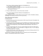
Page 32: ...n M3 screw with maximum thread depth in the unit of 5 mm is recommended 2 Connect the ground lug to chassis ground An 8 mm depth M3 screw with flat and lock washers is recommended 5 mm maximum thread depth in unit See Figure 4 showing location of mount ing holes for both package sizes note the additional length of package for cable version of switches 3 Connect the power supply to the unit via the...

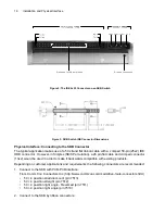
Page 33: ...nstructions Pinout Information for the Switch The signals for communication are connected via the 50 pin 25x2 IDE connector Power inputs are connected either through the 4 pin power pins on the 4x1 portion of the IDE connector or using the power pins located on the IDE 25x2 communications connector ...

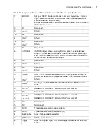
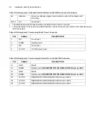
Page 34: ...ide B 42 485 Shield RS485 signal shield 43 Trigger Active low trigger signal TTL multi dropped pulled UP at slave with 100K 44 Attention Active low attention signal open collector pulled UP at master with 470 Ohms Table 2 Pin Assignment Simplex SK SP Emulation Parallel Interface on 25x2 IDE connector PIN SIGNAL DESCRIPTION 13 GND1 Shield 14 DGND2 Digital ground RESERVED FOR SK SP EMULATION Power o...

Page 35: ...lation mode i e this acts the same as the RESET line defined in the SK SP manual when the unit is wired as per this table 31 GND1 Shield 32 DGND2 Digital ground RESERVED FOR SK SP EMULATION Power on 2x25 33 5 VDC2 RESERVED FOR SK SP EMULATION Power on 2x25 34 D7 Data line 7 35 5 VDC2 RESERVED FOR SK SP EMULATION Power on 2x25 36 5 VDC2 RESERVED FOR SK SP EMULATION Power on 2x25 37 NC No connect 38...

Page 36: ...OBE signal 26 D5 Data line 5 27 GND1 Shield 28 D6 Data line 6 29 GND1 Shield 30 HOME Home input low sends the switch to the home position in Simplex SK SP emulation mode Replaces RESET line in emulation mode 31 GND1 Shield 32 DGND2 Digital ground RESERVED FOR SK SP EMULATION Power on 2x25 33 5 VDC2 RESERVED FOR SK SP EMULATION Power on 2x25 34 D7 Data line 7 35 5 VDC2 RESERVED FOR SK SP EMULATION ...

Page 37: ...ector PIN SIGNAL DESCRIPTION 1 NC No connect 2 DGND Digital ground 3 NC No connect 4 5V DC 5 VDC power input Table 5 Pin Assignment Power using the Power Pins on the 25x2 IDE Connector PIN SIGNAL DESCRIPTION 13 GND Shield 14 DGND Digital ground RESERVED FOR SK EMULATION Power on 2x25 31 GND Shield 32 DGND Digital ground RESERVED FOR SK EMULATION Power on 2x25 33 5 VDC RESERVED FOR SK EMULATION Pow...

Page 38: ...interfaces are also located on the IDE 2x25 connector Two modes of implementation Simplex and Enhanced are offered with the tradeoff being functionality versus complexity of imple mentation The Simplex parallel interface is unidirectional where data is presented and strobed in and the Enhanced parallel interface is bi directional packet based Examples of system level reasons for leveraging the Sim...

Page 39: ...hen the SKB is expected to operate over a wide temperature range or is located at a distance from the power source i e applications where system conditions are such that the voltage drop over the harness might exceed the SKB switch specifications 2 Only one of the two means of power connection should be employed at one time Architecture Overview of the RS485 Serial and Enhanced Parallel Interfaces...

Page 40: ...the SKB switch for the purposes of returning query data Response packets have an identical format as a standard command packet with the MSB of the opcode byte set If for example an opcode of 0x01h was sent to the SKB switch and this opcode represented a query the response packet would have an opcode of 0x81h The length byte of a response packet represents the total length of the parameter response...

Page 41: ...ation of serial and parallel interface is not supported Connecting Multiple Switches using the RS485 Interface Up to 31 RS485 unit loads can be connected to the differential bus Therefore up to 30 SKB switches and one master controller can be used to construct an RS485 network Exceeding the limit of 31 devices excessively loads the RS485 drivers and attenuates the differential signal The conse que...

Page 42: ...able length specified for RS485 buses is 1219 meters 4000 feet Generally the longer the cable length the slower the data transmission rate All applicable data baud rates used by the SKB switch operate over the maximum cable length when proper termination is used and the number of nodes does not exceed 31 Addressing using the RS485 Serial Interface The addresses are outlined in Table 7 Each SKB swi...

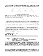
Page 43: ...ved following transmission of a data packet with a specified timeout period the sender needs to re transmit the data packet An ACK packet consists of a standard RS485 packet without a length byte any data payload bytes or CRC bytes The type byte is defined as an ACK 1 The ACK packet is shown in Figure 7 Figure 7 RS485 ACK Packet This ACK cycle is reversed when response data packets are sent from t...

Page 44: ...acket is received within a particular period following transmission of the last RS485 packet byte retransmit the original RS485 packet Typical protocol is shown in Figure 8 Figure 8 RS485 Network Implementation Transmit DATA packet to SKB slave ACK packet received before timeout period expired Response DATA packet required from SKB slave Response DATA packet received before timeout period expired ...

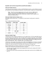
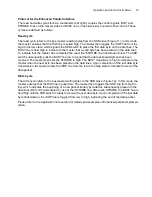
Page 45: ...mits channel numbers to be strobed in using the STROBE line As a reference for SK SP users the typical method of interface to a host controller for the SK SP Series Fiberoptic Switch is shown below for reference Figure 9 Typical Controller Connections Simultaneous operation of serial and parallel interface is not supported Simplex Parallel Interface Pin Functional Description Data Lines D0 to D6 V...

Page 46: ...positions A change on the data lines has no effect until there is a high to low transition on the Strobe line The Reset line also has no effect unless it is held low while the Strobe line has a high to low transition Busy Output Line The Busy line provides an indication of the switching mechanism state The line is low when the switch is idle and high when the switching mechanism is moving to anoth...

Page 47: ...igh if the reset function cannot verify the position of the switching mechanism Figure 10 Figure 10 Timing Diagram Timing Key The timing key symbols and values are listed in Table 10 Table 10 Timing Key Symbol Minimum Maximum tdh data hold time 20 µs tstr strobe pulse width 1 µs tmv switching cycle time 0 55 ms trh reset hold time 20 µs trst reset cycle time 1 1 s Busy Error ...

Page 48: ...basis using the BUSY output line of the SKB switch as the primary mechanism of controlling the data transfer rate By using control signals the actual signal timing can vary within defined tolerances according to the avail ability of the SKB switch which is indicated with a low level BUSY signal The primary control signals of the master are the SOP and STROBE lines Transitions of the SOP line are u...

Page 49: ... SOP command is with drawn or the communication sequence will be aborted The master is responsible for controlling the SOP line STROBE Input Line The STROBE line is used to signal the SKB switch to read data from or write data to the data lines A change on the data lines has no effect until there is a high to low transition on the STROBE line The STROBE line is driven by the master for both transm...

Page 50: ...nal that the data acknowledgment has been received The master then sets the STROBE to high The BUSY transitions to high to indicate to the master when the next byte has been placed on the data lines Upon completion of the last data byte transmission the master resets the SOP line from the low to the high state to indicate the end of the data packet Write Cycle The write cycle refers to the bus mas...

Page 51: ...P No Interface Idle Interface Idle R W SOP Packet Bytes to read No Reset SOP SOP Yes No BUSY Asserted Yes No BUSY Asserted No BUSY Reset Assert Busy Write Next Packet Byte to Data Bus Reset Busy Busy Busy STB Assert Strobe Read Data Byte Yes STB Reset Strobe More Yes Yes SOP Asserted No BUSY Asserted Yes No ...

Page 52: ...us Assert SOP Assert Strobe Reset Busy Assert Busy More Packet Bytes to send Interface Idle Save Packet Byte Interface Idle Yes Reset SOP SOP Busy Busy R W STB STROBE Asserted Yes No No BUSY Reset STB Yes No BUSY Asserted SOP Reset Strobe Yes No BUSY Asserted Yes No Read Packet Byte Assert Busy Busy Yes No BUSY Asserted ...

Page 53: ...38 Operation and Control Instructions ...

Page 54: ...ly to the Enhanced Parallel Interface and the RS485 Serial interface only Common Commands SKB common commands refer to those operations and queries common to most switch modules and instruments These commands represent the core functionality of the instrument module ...

Page 55: ...ardware reset is generated by the microcontroller On wakeup non latching switches move to the Reset position factory default is a null connect channel but this can have been changed by the user and latching switches stay on the same channel Also see the SWITCH command which can be used to send individual switches to the reset position Parameters NA Parameter Description NA OPCODE Length Parameters...

Page 56: ... are zero padded Core_Ver unsigned eight bit array of two elements A pair of two eight bit integers 0 to 255 representing the core firmware version The first element corresponds to the major version and the second to the minor version for example 1 10 Unused bytes are zero padded App_Ver unsigned eight bit array of two elements A pair of two eight bit integers 0 to 255 representing the application...

Page 57: ...eared The light emitting diode produces an amber light if this bit is set OPP OPERATION IN PROGRESS bit 4 This bit indicates that a critical operation is in process It is cleared when the operation is complete Note In the absence of alarm or error condition the light emitting diode stays green In the presence of both these conditions the light emitting diode reports the error condition by turning ...

Page 58: ... least 10 seconds It is cleared when the temperature falls below the high temperature threshold CFO CONFIGURATION OVERFLOW bit 12 This bit indicates that user configuration commands have been executed more than 50 000 times This bit is not cleared when the configuration com mand counter exceeds 50 000 This bit can only be cleared at the JDS Uniphase factory Description Query the alarm register val...

Page 59: ... last error message in the error queue Parameters NA Parameter Description NA OPCODE Length Parameters 0x04 0x00 OPCODE Length Parameters 0x84 0x01 U8 Error_code Error_Code unsigned eight bit Error code represents the last error that occurred as indicated in the following table ...

Page 60: ...0x0E Communication receive run on condition 15 0x0F Communication transmit run on condition 16 0x10 Communication invalid transmit operation initiated by master 17 0x11 Reserved 18 0x12 Communication invalid STROBE received 19 0x13 RS485 link layer packet CRC mismatch 20 0x14 RS485 invalid link layer packet length 21 0x15 RS485 invalid link layer packet type 22 0x16 RS485 invalid source address 23...

Page 61: ...46 Commands EQCLEAR Command packet Description Erase all entries in the error queue Parameters NA Parameter Description NA OPCODE Length Parameters 0x05 0x00 ...

Page 62: ...Parameters 0x86 0x06 U16 Hi_temp U16 Low_temp U16 Temp Hi_temp unsigned 16 bit Configured high temperature threshold 234 358 K Low_temp unsigned 16 bit Configured low temperature threshold 233 357 K Temp unsigned 16 bit Actual ambient temperature 233 358 K Temperature C Temperature K 273 All temperature information is referenced in degrees Kelvin Conversions are as follows 1 C 1 K and 0 C 273 K ap...

Page 63: ...second timer index 0 to 999 Sec unsigned eight bit The current second timer index 0 to 59 Min unsigned eight bit The current minute timer index 0 to 59 Hour unsigned 16 bit The current hour timer index 0 to 8759 Year unsigned eight bit The current year timer index 0 to 255 The system timer is returned as seven bytes as described previously These bytes can be extracted into a C structure for exampl...

Page 64: ...Commands 49 RESET_STIMER Command packet Description Reset the system timer to 0 Parameters NA Parameter Description NA OPCODE Length Parameters 0x0C 0x00 ...

Page 65: ...h unsigned eight bit Logical switch number upon which to perform action for example 1 to 4 Input unsigned eight bit Input channel to connect for example 1 on a 1xN switch Output unsigned eight bit Output channel to connect specified input chan nel where 0 reset position factory configured to be a null connect but this can have been changed by user 1 to 200 output channel number 254 previous channe...

Page 66: ...nsigned eight bit input channel number OPCODE Length Parameters 0x21 0x02 U8 Switch U8 Input Switch unsigned eight bit Logical switch number upon which to read infor mation for example 1 to 4 Input unsigned eight bit Input channel to find connection of OPCODE Length Parameters 0xA1 0x01 U8 Output Output unsigned eight bit The output channel connected to the input chan nel specified ...

Page 67: ...escription Query number of logical switches Parameters NA Parameter Description NA OPCODE Length Parameters 0x22 0x00 OPCODE Length Parameters 0xA2 0x01 U8 Switches Switches unsigned eight bit The number of logical switches in the module for example 1 to 4 ...

Page 68: ...nd the switch back to the state it was in prior to reset Parameters NA Parameter Description NA OPCODE Length Parameters 0x24 0x00 OPCODE Length Parameters 0xA4 0x05 to 0x141 1 5 U8 Opcode U8 Len U8 Sw_Id U8 Cur_In U8 Cur_Out Opcode unsigned eight bit SWITCH command opcode 0x20 Sw_Id unsigned eight bit Switch number 1 to 4 Cur_In unsigned eight bit Current input channel of the switch 1 to 2 Cur_Ou...

Page 69: ...ription NA OPCODE Length Parameters 0x25 0x00 OPCODE Length Parameters 0xA5 0x01 to 0x041 U8 Sw1_Result U8 Sw2_Result U8 Sw3_Result U8 Sw4_Result Sw1_Result unsigned eight bit Self test result 0 1 where 0 pass and 1 fail Sw2_Result unsigned eight bit Self test result 0 1 where 0 pass and 1 fail if necessary Sw3_Result unsigned eight bit Self test result 0 1 where 0 pass and 1 fail if necessary Sw4...

Page 70: ... switches in the module for later recall at one of 10 locations Parameters Location Parameter Description Location unsigned eight bit Memory location to save state OPCODE Length Parameters 0x26 0x01 U8 Location Location unsigned eight bit Memory location of state data 0 to 9 ...

Page 71: ...t settings These commands provide additional functionality than is available on current instrument modules Description Recall a module state previously saved Parameters Location Parameter Description Location unsigned eight bit memory location OPCODE Length Parameters 0x27 0x01 U8 Location Location unsigned eight bit Memory location of state data 0 to 9 ...

Page 72: ...ption NA OPCODE Length Parameters 0x23 0x00 OPCODE Length Parameters 0xA3 0x04 to 0x0F1 1 4 U8 Sw_Id U8 Sw_Type U8 Max_In U8 Max_Out Sw_Id unsigned eight bit Logical switch identification number 1 to 4 Sw_Type unsigned eight bit Physical switch type 0 motor or 1 relay Max_In unsigned eight bit Maximum number of inputs of the switch 1 to 2 Max_Out unsigned eight bit Maximum number of outputs of the...

Page 73: ...pproximately 1 F 0 55 K and 0 F 255 37 K Description Set the upper temperature threshold Parameters Temp Parameter Description Temp unsigned 16 bit The K high temperature threshold that if exceeded causes the OT alarm register bit to be set OPCODE Length Parameters 0x07 0x02 U16 Hi_temp Hi_temp unsigned 16 bit High temperature threshold 234 to 353 K ...

Page 74: ... the lower temperature threshold Parameters Temp Parameter Description Temp unsigned eight bit The K low temperature threshold that if exceeded causes the UT alarm register bit to be set OPCODE Length Parameters 0x08 0x02 U16 Low_temp Low_temp unsigned 16 bit Low temperature threshold 233 to 352 K ...

Page 75: ...itch specified Parameters Switch Parameter Description Switch unsigned eight bit logical switch OPCODE Length Parameters 0x30 0x01 U8 Switch Switch unsigned eight bit Logical switch number 1 to 4 OPCODE Length Parameters 0xB0 0x01 U8 Spares Spares unsigned eight bit The number of spare channels currently config ured for the switch ...

Page 76: ...unsigned eight bit channel number to be replaced Spare unsigned eight bit factory spare number OPCODE Length Parameters 0x33 0x3 U8 Switch U8 Output U8 Spare Switch unsigned eight bit Logical switch number 1 to 4 Output unsigned eight bit The replaced output channel 1 to 200 Spare unsigned eight bit The factory spare number used for the replace ment 1 to 200 This command resets the switch ...

Page 77: ...cription Switch unsigned eight bit switch number Output1 unsigned eight bit first output channel Output2 unsigned eight bit second output channel OPCODE Length Parameters 0x34 0x03 U8 Switch U8 Output1 U8 Output2 Switch unsigned eight bit Logical switch number 1 to 4 Output1 unsigned eight bit The first output channel 1 to 200 Output2 unsigned eight bit The second output channel 1 to 200 This comm...

Page 78: ...s Switch Parameter Description Switch unsigned eight bit switch number OPCODE Length Parameters 0x35 0x01 U8 Switch Switch unsigned eight bit Logical switch number 1 to 4 OPCODE Length Parameters 0xB5 0x01 U8 Latching_Status Latching_Status unsigned eight bit The status of the switch 1 latch ing 0 non latching ...

Page 79: ...ted switch Parameters Switch Parameter Description Switch unsigned eight bit switch number OPCODE Length Parameters 0x36 0x01 U8 Switch Switch unsigned eight bit Logical switch number 1 to 4 OPCODE Length Parameters 0xB6 0x01 U8 Output_Channel Output_Channel unsigned eight bit The output channel associated with the reset position 0 to 200 ...

Page 80: ...meters Reset_Channel Switch Parameter Description Reset_Channel unsigned eight bit Output channel number to be associated with the reset channel Switch unsigned eight bit switch number OPCODE Length Parameters 0x37 0x02 U8 Switch U8 Reset_Channel Switch unsigned eight bit Logical switch number 1 4 Reset_Channel unsigned eight bit The output channel to be associated with the reset position 0 to 200...

Page 81: ... Parameter Description Switch unsigned eight bit switch number OPCODE Length Parameters 0x38 0x01 U8 Switch Switch unsigned eight bit Logical switch number 1 to 4 This command resets the switch The setting is modified with the MODIFY_SPEED RESET_CHANNEL REPLACE and SWAP_CHANNEL commands Commands are reset to factory defaults ...

Page 82: ...ight bit switch number OPCODE Length Parameters 0x39 0x01 U8 Switch Switch unsigned eight bit Logical switch number 1 to 4 OPCODE Length Parameters 0xB9 0x01 U8 Speed Speed unsigned eight bit The speed setting of the switch 1 to 5 The speed setting of the switch 1 5 where 1 is the slowest speed and 5 the fastest Only speeds 1 and 5 are implemented ...

Page 83: ... bit switch number Speed unsigned eight bit speed setting for specified switch OPCODE Length Parameters 0x3A 0x02 U8 Switch U8 Speed Switch unsigned eight bit Logical switch number 1 to 4 Speed unsigned eight bit The speed setting of the switch 1 to 5 The speed setting of the switch 1 5 where 1 is the slowest speed and 5 the fastest Only speeds 1 and 5 are implemented ...

Page 84: ...U8 Switch U8 Start U8 Destination Parameter Description Switch unsigned eight bit switch number Start unsigned eight bit output channel to begin measurement Destination unsigned eight bit destination output channel OPCODE Length Parameters 0x3B 0x03 U8 Switch U8 Start U8 Destination Switch unsigned eight bit Logical switch number 1 to 4 Start unsigned eight bit The output channel of the specified ...

Page 85: ...ch Parameters Address Parameter Description Address unsigned eight bit network address OPCODE Length Parameters 0x3D 0x01 U8 Address Address unsigned eight bit Network address 1 to 31 NOTE The module is factory configured with address unless specified other wise Address 0 reserved for master controller ...

Page 86: ...Response packet Description Query the RS485 network address of the device Parameters NA Parameter Description NA OPCODE Length Parameters 0x3E 0x00 OPCODE Length Parameters 0xBE 0x01 U8 Address Address unsigned eight bit Network address 1 to 31 ...

Page 87: ...of the data portion Param1 Param2 Param3 unsigned eight bits first second and third parameter of the selected command number of parameters ranges from 0 to 3 depending of the selected command Note that the default opcode is for reset 0x00 OPCODE Length Parameters 0x3F 0x02 to 0x0A1 U8 Opcode U8 Length U8 Param1 U8 Param2 U8 Param3 Opcode unsigned eight bit Opcode of the command selected to be exe ...

Page 88: ...ODE Length Parameters 0x40 0x00 OPCODE Length Parameters 0xC0 0x02 to 0x0A1 U8 Opcode U8 Length U8 Param1 U8 Param8 Opcode unsigned eight bit Opcode of the command selected to be exe cuted as part of the trigger command 0x20 to 0x27 Length unsigned eight bit The length of the data portion of the command packet Param1 Param8 unsigned eight bit Data payload bytes specific to the opcode specified ...

Page 89: ...ion Modify the baud rate of the device Parameters Baud_Rate Parameter Description Baud_Rate Baud rate code OPCODE Length Parameters 0x41 0x01 U8 Baud_Rate Baud_Rate unsigned eight bit Baud rate setting 0 4 defined as follows 0 2400 baud 1 4800 baud ...

Page 90: ...scription Query the baud rate of the device Parameters NA Parameter Description NA OPCODE Length Parameters 0x42 0x00 OPCODE Length Parameters 0xC2 0x01 U8 Baud_Rate Baud_Rate unsigned eight bit Baud rate setting 0 4 defined as follows 0 2400 baud 1 4800 baud ...

Page 91: ...76 Commands ...

Page 92: ... the entire RS 485 address range ie 1 31 to determine which addresses have active devices This is determined by receipt of a valid response to the query The master should build a list of used and unused RS 485 addresses 2 A new SKB switch with an address of 1 is added to the RS 485 network and powered up This will cause the ATTN to be asserted 3 The master recognizes that the ATTN line is asserted...

Page 93: ...ut signal is constantly monitored and the trigger line is asserted if the power exceeds tolerable thresholds 1 Set the trigger command to execute a SWITCH command to a channel which is intended to han dle high power input ie signal is attenuated after exiting the SKB switch 2 Tap input channel monitor signal power 3 During switching operations monitor the power of the incoming signal to ensure is ...

Page 94: ...te cycle These figures show the relationship between R W SOP and STROBE input lines and the BUSY output line during a five byte command packet write to the SKB Note that in each scenario illustrated the line toggling is identical and independent of the STROBE pulse time Figure 13 SKB enhanced mode 5 byte write master to slave high speed The following actions correspond to numbered events in Figure...

Page 95: ... held high to indicate to the master that a valid byte has been placed on the data lines The master reads the data lines and sets the STROBE line to low to indicate that the read is complete The SKB switch subsequently pulls the BUSY line low to signal that the data acknowledgment has been received The master then sets the STROBE to high The BUSY transitions to high to indicate to the master when ...

Page 96: ... indicate the first byte of the packet has been written to the data bus 4 Binary data is read from the data lines D0 to D7 and the STROBE line is asserted low to indi cate to the SKB switch that the byte was read 5 The BUSY line is de asserted low to indicate to the master that the SKB switch is ready to send another byte 6 The STROBE is de asserted high to indicate to the SKB switch that the mast...

Page 97: ...pack ets and generating a CRC 16 The SKB implements a differential signal RS 485 network protocol which is capable of connecting 32 unit load devices one bus master and up to 31 SKB slaves The network layer of the RS 485 proto col is handled by transceivers connected to the UART of the SKB Transmitting and receiving RS 485 differential data is transparent to the user The remaining network protocol...

Page 98: ...preted as a valid packet byte rather than a SOH 1 byte DEST The destination device address where the packet is being sent All other devices will ignore the rest of the packet bytes 1 byte SRC The device address of the sender This byte is remembered and used to send ACK or response packets 1 byte TYPE Defines the purpose of the packet a value of 0 means this is a packet containing data and a value ...

Page 99: ...rfaces CRC Generation In the above example App Note RS485 Packet Example the CRC 16 value 0xF02A is appended to the end of the link layer packet prior to actually being transmitted by the master Because the CRC is a 16 bit value bytes are swapped high byte low byte as per the standard command packet byte order protocol described Byte Order on page 25 Using the above example the CRC value was calcu...

Page 100: ...AMPLE application note link layer packet example INPUTS unsigned char ptr pointer to link layer packet int count number of bytes in packet RETURNS int CRC value On WIN32 int is 32 bits CRC appears in the low order 16 bits SCOPE Global NOTES int calc_crc16 unsigned char ptr int count int crc i Initialize crc to 0 for XMODEM 1 for CCITT crc 0 cycle through all bytes and add to CRC while count 0 XOR ...

Page 101: ...n void unsigned char Packet 256 int crc Build RS 485 Link layer packet as per example Packet 0 0x81 SOH Packet 1 0x01 DEST Packet 2 0x00 SRC Packet 3 0x00 TYPE 0 DATA Packet 4 0x05 LEN low byte Packet 5 0x00 LEN high byte Packet 6 0x20 PAYLOAD 1 opcode Packet 7 0x03 PAYLOAD 2 length Packet 8 0x01 PAYLOAD 3 switch Packet 9 0x01 PAYLOAD 4 input Packet 10 0x02 PAYLOAD 5 output calculate the CRC crc c...

Page 102: ...is mode the SKB switch is functionally compatible to an SK switch The pins allocated to SK emulation are located in the center portion of the 2x25 connector allowing direct ribbon cable drop in to existing applications To connect an existing SK controller to a SKB II unit an adapter cable assembly is required The wir ing information is contained in Table 12 below An illustration of an SKB device w...

Page 103: ...2 21 9 GND Shield 22 10 D3 Data line 3 23 11 GND Shield 24 12 D4 Data line 4 POLARIZ ING KEY POLARIZ ING KEY 25 13 STROBE STROBE input active low read data lines high ignore state of data lines Note The home line is also read in via the STROBE signal 26 14 D5 Data line 5 27 15 GND Shield 28 16 D6 Data line 6 29 17 GND Shield 30 18 HOME Home input low sends the switch to the home posi tion Note the...

Page 104: ...ring SKB via the signal connector the cable length may not exceed 8 inches An adapter cable assembly is available from JDS Uniphase under part number ED0 A 00 as shown in Figure 18 Figure 18 SKB to SK SP Adapter Cable Assembly Drawing ...

Page 105: ... for the purpose of evaluation of the SKB product Setting the Computer to EPP Mode In order to interface with the SKB switch via the computer parallel port it is necessary to make the data lines bi directional accomplished by using a parallel port operating in EPP mode To set the PC to EPP mode 1 Use the PC operating manual and configure the parallel port for EPP entering into the computers BIOS m...

Page 106: ...ector interface That vari ant is described in this application note All control information contained in the body of this manual applies to this variant Hence this appli cation note addresses physical features only Table 13 Cable Wiring for Printer Port LPT2 Use Printer Signal Name Register Bit Hex Address Number PC Connector Pin SKB Pin SKB Signal Name Line Feed 37A 11 14 20 STROBE Data 0 378 0 2...

Page 107: ...irst connector is a 25 pin D subminiature connector used by the parallel interface The second connector is a 9 pin D subminiature connector which provides for the power connection and the RS485 Serial interface A separate chassis ground connection point also is provided Figure 19 Connector and Port Locations Figure 20 Connector and Port Locations ...

Page 108: ...er and Serial Interface Connector The 9 pin D subminiature connector is used for power and serial RS485 interface The signals for power and communication are connected via the D subminiature 9 pin serial connec tor Figure 23 and Table 14 Figure 22 Pin Assignment ...

Page 109: ...r Active low trigger signal transis tor to transistor logic TTL multi ended pulled UP at slave with 100 K This line is driven by the host processor mas ter to indicate to the slaves that a trigger based action is to be executed on the falling edge of this signal This action is usually pre conditioned by a request to the applicable slaves Pin 5 Attention Active low attention signal open collector p...

Page 110: ...ad write driven by master read and write cycles 13 GND Shield 14 D0 Data line 0 input least significant bit LSB 15 GND Shield 16 D3 Data line 3 17 D4 Data line 4 18 GND Shield 19 D7 Data line 7 most significant bit MSB 20 STROBE STROBE input active low high to low pulse read data lines and home line high ignore state of data lines and home line This line is internally pulled high via 10 K ohm resi...

Page 111: ...96 Application Notes ...

Page 112: ...nd serial number of the unit Detailed description of the defects or problems Owner s name address and contact phone number Date of purchase Shipping a Unit Perform the following steps to ship the unit 1 Wear an anti static wrist strap and work in an ESD controlled area 2 Pack the unit in the original shipping container and packing material 3 When these materials are unavailable the following guide...

Page 113: ...98 Service ...

Reviews: