


S p e z i a l e l e k t r o n i k G m b H
iseg Spezialelektronik GmbH
Email: [email protected]
Phone ++ 49 (0)351 / 26 996 - 0
Bautzner Landstr 23
http://www.iseg-hv.com
Fax
++ 49 (0)351 / 26 996 - 21
D - 01454 Radeberg / Rossendorf
Germany
3
3. Handling
The supply voltages and the CAN interface is connected to the module via a 96-pin connector on the
rear side of the module.
The maximum output current and voltage for the channels 0 to 16 are defined through the position of
the corresponding potentiometer I
max
resp. V
max
.
It is possible to measure the hardware limits, which has been set with reference to the maximum
possible current resp. voltage at the according 2-pin socket. 100 % I
max
resp. V
max
corresponds to
2,5 V. The output current and voltage will be limited to the setting value after it exceeds the threshold
and the corresponding green LED on the front panel is ‘OFF‘.
At the bottom on the right side of the front panel is the 2-pin LEMO socket for the safety loop. This
connector is installed in-line with the upper (SL PIN 22) and lower SL contacts (SL PIN 30) on the HV
connector (see the pin designation on the front panel or in the pin assignment). The safety loop will be
closed by connection of the load with help of a connection between PIN 22 and 30 on the HV cable
side of the connector. If the safety loop is active then output voltage on all channels is present only if
a current of any polarity is flowing in a range of 5 to 20 mA (i.e. safety loop closed). If the safety loop
is opened during operation then the output voltages on all channels are shut off without ramp and the
corresponding bit in the ‘Status module’ will be cancelled. After the loop will be closed again the
channels must be switched ‘ON’ and a new set voltage must be given before it is able to offer an
output voltage.
The pins of the loops are potential free, the internal voltage drop is ca. 3 V. Coming from the factory
the safety loops are not active (the corresponding bit is always set). Removing of an internal jumper
on the rear side of the unit makes the loops active.
(s. App. B “Operator’s Manual CAN-Interface”).
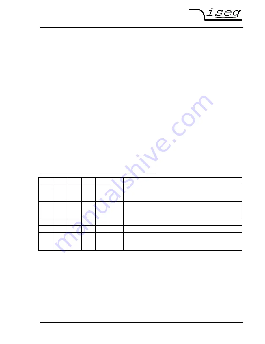
Pin assignment 96-pin connector according to DIN 41612:
PIN
PIN
PIN
Data
a1
b1
c1
+5V
a3
b3
c3
+24V
a5
b5
c5
GND
a11
@CAN_GND
⎫
b11
@CANL
⎬
potential free
c11
@CANH
⎭
a13
RESET
b13
OFF with ramp (e.g. at power fail)
a30
A4
b30
A5
c30
GND
⎫
a31
A2
b31
A3
c31
GND
⎬
Address
field
a32
A0
b32
A1
c32
GND
⎭
module address ( A0 ... A5)
The hardware signal “OFF with ramp” (Pulse High-Low-High, pulse width
≤
100 µs) on pin b13 will be
shut off the output voltage for all channels with a ramp analogue to the Group access “Channel
ON/
OFF”
. The ramp speed is defined to V
OUTmax
/ 50 s. This is the actually module ramp speed after
“OFF with ramp”.
With help of the Group access “Channel
ON
/OFF
”
all channels are switched “ON” again.
With the address field a30/b30 ..... a32/b32 the module address will be coded.
(see item 4.4, description 11bit-Identifier).
Connected to GND
⇒
A(n) = 0 ; contact open
⇒
A(n) = 1