background image

Developer’s Manual

January, 2004

177

Intel XScale® Core


Developer’s Manual

Optimization Guide

A.2.1.2.

The Intel XScale

®

 Core Pipeline Organization

The Intel XScale

®

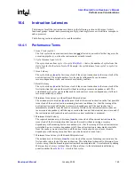
 core single-issue superpipeline consists of a main execution pipeline, MAC 

pipeline, and a memory access pipeline. These are shown in 

Figure A-1

, with the main execution 

pipeline shaded.

Table A-1

 gives a brief description of each pipe-stage.

Figure A-1. 

The Intel XScale

®

 Core RISC Superpipeline

F1

F2

ID

RF

X1

X2

XWB

M1

M2

Mx

D1

D2

DWB

Main execution pipeline

MAC pipeline

Memory pipeline

Table A-1. 

Pipelines and Pipe stages

Pipe / Pipestage

Description

Covered In

Main Execution Pipeline 

Handles data processing instructions

Section A.2.3

IF1/IF2

Instruction Fetch

ID

Instruction Decode

RF

Register File / Operand Shifter

X1

ALU Execute

X2

State Execute

XWB

Write-back

Memory Pipeline

Handles load/store instructions

Section A.2.4

D1/D2

Data Cache Access

DWB

Data cache writeback

MAC Pipeline

Handles all multiply instructions

Section A.2.5

M1-M5 

Multiplier stages

MWB (not shown)

MAC write-back - may occur during M2-M5

Summary of Contents for XScale Core

Page 1: ...Intel XScale Core Developer s Manual January 2004 Order Number 273473 002 ...

Page 2: ...ANY PROPOSAL SPECIFICATION OR SAMPLE Intel disclaims all liability including liability for infringement of any proprietary rights relating to use of information in this specification No license express or implied by estoppel or otherwise to any intellectual property rights is granted herein Copyright Intel Corporation 2004 AlertVIEW i960 AnyPoint AppChoice BoardWatch BunnyPeople CablePort Celeron ...

Page 3: ...amming Model 21 2 1 ARM Architecture Compatibility 21 2 2 ARM Architecture Implementation Options 21 2 2 1 Big Endian versus Little Endian 21 2 2 2 26 Bit Architecture 21 2 2 3 Thumb 21 2 2 4 ARM DSP Enhanced Instruction Set 22 2 2 5 Base Register Update 22 2 3 Extensions to ARM Architecture 23 2 3 1 DSP Coprocessor 0 CP0 23 2 3 1 1 Multiply With Internal Accumulate Format 24 2 3 1 2 Internal Accu...

Page 4: ... 4 2 5 Parity Protection 50 4 2 6 Instruction Fetch Latency 51 4 2 7 Instruction Cache Coherency 51 4 3 Instruction Cache Control 52 4 3 1 Instruction Cache State at RESET 52 4 3 2 Enabling Disabling 52 4 3 3 Invalidating the Instruction Cache 53 4 3 4 Locking Instructions in the Instruction Cache 54 4 3 5 Unlocking Instructions in the Instruction Cache 55 5 Branch Target Buffer 57 5 1 Branch Targ...

Page 5: ...Operations 89 7 2 10 Register 9 Cache Lock Down 90 7 2 11 Register 10 TLB Lock Down 91 7 2 12 Register 11 12 Reserved 91 7 2 13 Register 13 Process ID 91 7 2 13 1 The PID Register Affect On Addresses 92 7 2 14 Register 14 Breakpoint Registers 93 7 2 15 Register 15 Coprocessor Access Register 94 7 3 CP14 Registers 96 7 3 1 Performance Monitoring Registers 96 7 3 1 1 XSC1 Performance Monitoring Regi...

Page 6: ... Introduction 122 9 3 1 Halt Mode 122 9 3 2 Monitor Mode 122 9 4 Debug Control and Status Register DCSR 123 9 4 1 Global Enable Bit GE 124 9 4 2 Halt Mode Bit H 124 9 4 3 SOC Break B 124 9 4 4 Vector Trap Bits TF TI TD TA TS TU TR 125 9 4 5 Sticky Abort Bit SA 125 9 4 6 Method of Entry Bits MOE 125 9 4 7 Trace Buffer Mode Bit M 125 9 4 8 Trace Buffer Enable Bit E 125 9 5 Debug Exceptions 126 9 5 1...

Page 7: ...n Cache Overview 154 9 14 2 LDIC JTAG Command 155 9 14 3 LDIC JTAG Data Register 155 9 14 4 LDIC Cache Functions 156 9 14 5 Loading Instruction Cache During Reset 158 9 14 6 Dynamically Loading Instruction Cache After Reset 160 9 14 6 1 Dynamic Download Synchronization Code 162 10 Performance Considerations 163 10 1 Interrupt Latency 163 10 2 Branch Prediction 164 10 3 Addressing Modes 164 10 4 In...

Page 8: ...ecks 183 A 3 1 2 Optimizing Branches 184 A 3 1 3 Optimizing Complex Expressions 186 A 3 2 Bit Field Manipulation 187 A 3 3 Optimizing the Use of Immediate Values 188 A 3 4 Optimizing Integer Multiply and Divide 189 A 3 5 Effective Use of Addressing Modes 190 A 4 Cache and Prefetch Optimizations 191 A 4 1 Instruction Cache 191 A 4 1 1 Cache Miss Cost 191 A 4 1 2 Round Robin Replacement Cache Policy...

Page 9: ...A 5 1 2 Scheduling Load and Store Multiple LDM STM 211 A 5 2 Scheduling Data Processing Instructions 212 A 5 3 Scheduling Multiply Instructions 213 A 5 4 Scheduling SWP and SWPB Instructions 214 A 5 5 Scheduling the MRA and MAR Instructions MRRC MCRR 215 A 5 6 Scheduling the MIA and MIAPH Instructions 216 A 5 7 Scheduling MRS and MSR Instructions 217 A 5 8 Scheduling CP15 Coprocessor Instructions ...

Page 10: ...anization 62 6 2 Mini Data Cache Organization 63 6 3 Locked Line Effect on Round Robin Replacement 74 9 1 SELDCSR 139 9 2 DBGTX 141 9 3 DBGRX 142 9 4 Message Byte Formats 148 9 5 Indirect Branch Entry Address Byte Organization 151 9 6 High Level View of Trace Buffer 152 9 7 LDIC JTAG Data Register Hardware 155 9 8 Format of LDIC Cache Functions 157 9 9 Code Download During a Cold Reset For Debug 1...

Page 11: ...ormat when Accessing CP14 79 7 3 CP15 Registers 80 7 4 ID Register 81 7 5 Cache Type Register 82 7 6 ARM Control Register 83 7 7 Auxiliary Control Register 84 7 8 Translation Table Base Register 85 7 9 Domain Access Control Register 85 7 10Fault Status Register 86 7 11Fault Address Register 86 7 12Cache Functions 87 7 13TLB Functions 89 7 14Cache Lockdown Functions 90 7 15Data Cache Lock Register ...

Page 12: ...uffer Register Summary 145 9 16Checkpoint Register CHKPTx 146 9 17TBREG Format 147 9 18Message Byte Formats 148 9 19LDIC Cache Functions 156 9 20Steps For Loading Mini Instruction Cache During Reset 159 9 21Steps For Dynamically Loading the Mini Instruction Cache 161 10 1Branch Latency Penalty 164 10 2Latency Example 166 10 3Branch Instruction Timings Those predicted by the BTB 167 10 4Branch Inst...

Page 13: ...e right to make changes to these specifications at any time without notice In particular descriptions of features timings and pin outs does not imply a commitment to implement them 1 1 1 How to Read This Document It is necessary to be familiar with the ARM Version 5TE Architecture in order to understand some aspects of this document Each chapter in this document focuses on a specific architectural...

Page 14: ... Version 5TE Specification Document Number ARM DDI 0100E This document describes Version 5TE of the ARM Architecture which includes Thumb ISA and ARM DSP Enhanced ISA ISBN 0 201 737191 StrongARM SA 1100 Microprocessor Developer s Manual Intel Order 278105 StrongARM SA 110 Microprocessor Technical Reference Manual Intel Order 278104 ...

Page 15: ...on even while the data cache is retrieving data from external memory a write buffer write back caching various data cache allocation policies which can be configured different for each application and cache locking All these features improve the efficiency of the memory bus external to the core The Intel XScale core has been equipped to efficiently handle audio processing through the support of 16...

Page 16: ...umulator and support for 16 bit packed data See Section 2 3 Extensions to ARM Architecture on page 2 23 for more details Figure 1 1 Architecture Features Write Buffer 8 entries Full coalescing Fill Buffer 4 8 entries Instruction Cache 32K or 16K bytes 32 ways Lockable by line IMMU 32 entry TLB Fully associative Lockable by entry DMMU 32 entry TLB Fully Associative Lockable by entry JTAG Debug Hard...

Page 17: ...ion Cache discusses this in more detail 1 2 2 4 Branch Target Buffer The Intel XScale core provides a Branch Target Buffer BTB to predict the outcome of branch type instructions It provides storage for the target address of branch type instructions and predicts the next address to present to the instruction cache when the current instruction address is that of a branch The BTB holds 128 entries Se...

Page 18: ...ing their clocking and managing their power These features are described in Section 7 3 CP14 Registers on page 7 96 1 2 2 8 Debug The Intel XScale core supports software debugging through two instruction address breakpoint registers one data address breakpoint register one data address mask breakpoint register and a trace buffer Chapter 9 Software Debug discusses this in more detail 1 2 2 9 JTAG T...

Page 19: ... is placed in the same write buffer entry as an existing store when the address of the new store falls in the 4 word aligned address of the existing entry This includes in PCI terminology write merging write collapsing and write combining Deassert This term refers to the logically inactive value of a signal or bit Flush A flush operation invalidates the location s in the cache by deasserting the v...

Page 20: ...20 January 2004 Developer s Manual Intel XScale Core Developer s Manual Introduction This Page Intentionally Left Blank ...

Page 21: ...ages 1 Kbyte a new instruction CLZ that counts the leading zeroes in a data value enhanced ARM Thumb transfer instructions and a modification of the system control coprocessor CP15 2 2 ARM Architecture Implementation Options 2 2 1 Big Endian versus Little Endian The Intel XScale core supports both big and little endian data representation The B bit of the Control Register Coprocessor 15 register 1...

Page 22: ...D is interpreted as a read operation by the MMU and is ignored by the data breakpoint unit i e PLD will never generate data breakpoint events PLD to a non cacheable page performs no action Also if the targeted cache line is already resident this instruction has no affect Both LDRD and STRD instructions will generate an alignment exception when the address bits 2 0 0b100 MCRR and MRRC are only supp...

Page 23: ... 40 bit accumulator and 8 new instructions Note Products using the Intel XScale core may extend the definition of CP0 If this is the case a complete definition can be found in the Intel XScale core implementation option section of the ASSP architecture specification For this very reason software should not rely on behavior that is specific to the 40 bit length of the accumulator since the length m...

Page 24: ...single 40 bit accumulator referred to as acc0 future implementations may define multiple internal accumulators The Intel XScale core uses opcode_3 to define six instructions MIA MIAPH MIABB MIABT MIATB and MIATT Table 2 1 Multiply with Internal Accumulate Format 31 30 29 28 27 26 25 24 23 22 21 20 19 18 17 16 15 14 13 12 11 10 9 8 7 6 5 4 3 2 1 0 cond 1 1 1 0 0 0 1 0 opcode_3 Rs 0 0 0 0 acc 1 Rm B...

Page 25: ...re sign extended and then added to the value in the 40 bit accumulator acc0 The instruction is only executed if the condition specified in the instruction matches the condition code status Table 2 2 MIA cond acc0 Rm Rs 31 30 29 28 27 26 25 24 23 22 21 20 19 18 17 16 15 14 13 12 11 10 9 8 7 6 5 4 3 2 1 0 cond 1 1 1 0 0 0 1 0 0 0 0 0 Rs 0 0 0 0 0 0 0 1 Rm Operation if ConditionPassed cond then acc0 ...

Page 26: ...be interpreted as signed data values The instruction is only executed if the condition specified in the instruction matches the condition code status Table 2 4 MIAxy cond acc0 Rm Rs 31 30 29 28 27 26 25 24 23 22 21 20 19 18 17 16 15 14 13 12 11 10 9 8 7 6 5 4 3 2 1 0 cond 1 1 1 0 0 0 1 0 1 1 x y Rs 0 0 0 0 0 0 0 1 Rm Operation if ConditionPassed cond then if bit 17 0 operand1 Rm 15 0 else operand1...

Page 27: ...0 and MRA has the same encoding as MRRC to coprocessor 0 These instructions move 64 bits of data to from ARM registers from to coprocessor registers MCRR and MRRC are defined in ARM s DSP instruction set Disassemblers not aware of MAR and MRA will produce the following syntax MCRR cond p0 0x0 RdLo RdHi c0 MRRC cond p0 0x0 RdLo RdHi c0 Table 2 5 Internal Accumulator Access Format 31 30 29 28 27 26 ...

Page 28: ...RdHi 31 30 29 28 27 26 25 24 23 22 21 20 19 18 17 16 15 14 13 12 11 10 9 8 7 6 5 4 3 2 1 0 cond 1 1 0 0 0 1 0 0 RdHi RdLo 0 0 0 0 0 0 0 0 0 0 0 0 Operation if ConditionPassed cond then acc0 39 32 RdHi 7 0 acc0 31 0 RdLo 31 0 Exceptions none Qualifiers Condition Code No condition code flags are updated Notes Instruction timings can be found in Section 10 4 4 Multiply Instruction Timings on page 10 ...

Page 29: ... a load operation misses the data cache cacheable data only Write through caching causes all store operations to be written to memory whether they are cacheable or not cacheable This feature is useful for maintaining data cache coherency The Intel XScale core also adds a P bit in the first level descriptors to allow an ASSP to identify a new memory attribute Refer to the Intel XScale core implemen...

Page 30: ...30 29 28 27 26 25 24 23 22 21 20 19 18 17 16 15 14 13 12 11 10 9 8 7 6 5 4 3 2 1 0 SBZ 0 0 Coarse page table base address P Domain SBZ 0 1 Section base address SBZ TEX AP P Domain 0 C B 1 0 Fine page table base address SBZ P Domain SBZ 1 1 Table 2 9 Second level Descriptors for Coarse Page Table 31 30 29 28 27 26 25 24 23 22 21 20 19 18 17 16 15 14 13 12 11 10 9 8 7 6 5 4 3 2 1 0 SBZ 0 0 Large pag...

Page 31: ...cal method to wait for CP15 update When setting multiple CP15 registers system software may opt to delay the assurance of their update This is accomplished by executing CPWAIT only after the sequence of MCR instructions Note The CPWAIT sequence guarantees that CP15 side effects are complete by the time the CPWAIT is complete It is possible however that the CP15 side effect will take place before C...

Page 32: ...ee Chapter 9 Software Debug Table 2 11 Exception Summary Exception Description Exception Typea a Exception types are those described in the ARM section 2 5 Precise Updates FAR Reset Reset N N FIQ FIQ N N IRQ IRQ N N External Instruction Prefetch Y N Instruction MMU Prefetch Y N Instruction Cache Parity Prefetch Y N Lock Abort Data Y N MMU Data Data Y Y External Data Data N N Data Cache Parity Data...

Page 33: ...the link register in abort mode is the address of the aborted instruction 4 Table 2 13 Encoding of Fault Status for Prefetch Aborts Priority Sources FS 10 3 0 a a All other encodings not listed in the table are reserved Domain FAR Highest Instruction MMU Exception Several exceptions can generate this encoding translation faults domain faults and permission faults It is up to software to figure out...

Page 34: ...anslation The status field is set to a predetermined ARM definition which is shown in Table 2 14 Encoding of Fault Status for Data Aborts on page 2 34 The Fault Address Register is set to the effective data address of the instruction and R14_ABORT is the address of the aborted instruction 8 Imprecise data aborts A data cache parity error is imprecise the extended Status field of the Fault Status R...

Page 35: ...lt occurs it will do so during the NOPs the data abort handler will see identical register and memory state as it would with a precise exception and so should be able to recover An example of this is shown in Example 2 2 on page 2 35 If a system design precludes events that could cause external aborts then such precautions are not necessary Multiple Data Aborts Multiple data aborts may be detected...

Page 36: ...ther it will be ignored and the loop will terminate normally 2 3 4 6 Debug Events Debug events are covered in Section 9 5 Debug Exceptions on page 9 126 Example 2 3 Speculatively issuing PLD R0 points to a node in a linked list A node has the following layout Offset Contents 0 data 4 pointer to next node This code computes the sum of all nodes in a list The sum is placed into R9 MOV R9 0 Clear acc...

Page 37: ...ress to a physical address Once translated the physical address is placed in the TLB along with the access rights and attributes of the page or section These translations can also be locked down in either TLB to guarantee the performance of critical routines The Intel XScale core allows system software to associate various attributes with regions of memory cacheable bufferable line allocate policy...

Page 38: ...er system software the new core attributes take advantage of encoding space in the descriptors that was formerly reserved 3 2 2 1 Page P Attribute Bit The P bit allows an ASSP to assign its own page attribute to a memory region This bit is only present in the first level descriptors Refer to the Intel XScale core implementation section of the ASSP architecture specification to find out how this ha...

Page 39: ...untered With this setting the processor will stall execution until the data access completes This guarantees to software that the data ac cess has taken effect by the time execution of the data access instruction completes External data aborts from such access es will be imprecise but see Section 2 3 4 4 for a method to shield code from this imprecision 0 1 N Y 1 0 Y Y Write Through Read Allocate ...

Page 40: ...che to keep external memory coherent by performing stores to both external memory and the cache A write back policy only updates external memory when a line in the cache is cleaned or needs to be replaced with a new line Generally write back provides higher performance because it generates less data traffic to external memory More details on cache policies may be gleaned from Section 6 2 3 Cache P...

Page 41: ...ed disabled independently The instruction cache can be enabled with the MMU enabled or disabled However the data cache can only be enabled when the MMU is enabled Therefore only three of the four combinations of the MMU and data mini data cache enables are valid The invalid combination will cause undefined results Table 3 4 Valid MMU Data mini data Cache Combinations MMU Data mini data Cache Off O...

Page 42: ... the MMU is disabled accesses to the instruction cache default to cacheable and all accesses to data memory are made non cacheable A recommended code sequence for enabling the MMU is shown in Example 3 1 on page 3 42 Example 3 1 Enabling the MMU This routine provides software with a predictable way of enabling the MMU After the CPWAIT the MMU is guaranteed to be enabled Be aware that the MMU will ...

Page 43: ...ception is reported as a data abort Note If exceptions are allowed to occur in the middle of this routine the TLB may end up caching a translation that is about to be locked For example if R1 is the virtual address of an interrupt service routine and that interrupt occurs immediately after the TLB has been invalidated the lock operation will be ignored when the interrupt service routine returns ba...

Page 44: ... Data TLB R1 and R2 contain the virtual addresses to translate and lock into the data TLB MCR P15 0 R1 C8 C6 1 Invalidate the data TLB entry specified by the virtual address in R1 MCR P15 0 R1 C10 C8 0 Translate virtual address R1 and lock into data TLB Repeat sequence for virtual address in R2 MCR P15 0 R2 C8 C6 1 Invalidate the data TLB entry specified by the virtual address in R2 MCR P15 0 R2 C...

Page 45: ...re it will wrap back to entry 0 upon the next translation A lock pointer is used for locking entries into the TLB and is set to entry 0 at reset A TLB lock operation places the specified translation at the entry designated by the lock pointer moves the lock pointer to the next sequential entry and resets the round robin pointer to entry 31 Locking entries into either TLB effectively reduces the av...

Page 46: ...46 January 2004 Developer s Manual Intel XScale Core Developer s Manual Memory Management This Page Intentionally Left Blank ...

Page 47: ...ds and one valid bit which is referred to as a line The replacement policy is a round robin algorithm and the cache also supports the ability to lock code in at a line granularity The instruction cache is virtually addressed and virtually tagged Note The virtual address presented to the instruction cache may be remapped by the PID register See Section 7 2 13 Register 13 Process ID on page 7 91 for...

Page 48: ...nagement Unit MMU is disabled or when the MMU is enable and the cacheable C bit is set to 1 in its corresponding page See Chapter 3 Memory Management for a discussion on page attributes Note that an instruction fetch may miss the cache but hit one of the fetch buffers When this happens the requested instruction will be delivered to the instruction decoder in the same manner as a cache hit 4 2 2 Op...

Page 49: ...in replacement algorithm This update may evict a valid line at that location 6 Once the cache is updated the eight valid bits of the fetch buffer are invalidated 4 2 4 Round Robin Replacement Algorithm The line replacement algorithm for the instruction cache is round robin Each set in the instruction cache has a round robin pointer that keeps track of the next line in that set to replace The next ...

Page 50: ...d the branch target buffer and then returning to the instruction that caused the prefetch abort exception A simplified code example is shown in Example 4 1 on page 4 50 A more complex handler might choose to invalidate the specific line that caused the exception and then invalidate the BTB If a parity error occurs on an instruction that is locked in the cache the software exception handler needs t...

Page 51: ...tion and invalidating are completed To achieve cache coherence instruction cache contents can be invalidated after code modification in external memory is complete Refer to Section 4 3 3 Invalidating the Instruction Cache on page 4 53 for the proper procedure in invalidating the instruction cache If the instruction cache is not enabled or code is being written to a non cacheable region software mu...

Page 52: ...ed and invalidated flushed 4 3 2 Enabling Disabling The instruction cache is enabled by setting bit 12 in coprocessor 15 register 1 Control Register This process is illustrated in Example 4 2 Enabling the Instruction Cache Example 4 2 Enabling the Instruction Cache Enable the ICache MRC P15 0 R0 C1 C0 0 Get the control register ORR R0 R0 0x1000 set bit 12 the I bit MCR P15 0 R0 C1 C0 0 Set the con...

Page 53: ...nvalidate command This unlock command can also be found in Table 7 14 Cache Lockdown Functions on page 7 90 There is an inherent delay from the execution of the instruction cache invalidate command to where the next instruction will see the result of the invalidate The following routine can be used to guarantee proper synchronization The Intel XScale core also supports invalidating an individual l...

Page 54: ...nto the cache the code being locked into the cache must be cacheable 8 the instruction cache must be enabled and invalidated prior to locking down lines Failure to follow these requirements will produce unpredictable results when accessing the instruction cache System programmers should ensure that the code to lock instructions into the cache does not reside closer than 128 bytes to a non cacheabl...

Page 55: ...d for the instruction cache Writing to coprocessor 15 register 9 unlocks all the locked lines in the instruction cache and leaves them valid These lines then become available for the round robin replacement algorithm See Table 7 14 Cache Lockdown Functions on page 7 90 for the exact command Example 4 4 Locking Code into the Cache lockMe This is the code that will be locked into the cache mov r0 5 ...

Page 56: ...56 January 2004 Developer s Manual Intel XScale Core Developer s Manual Instruction Cache This Page Intentionally Left Blank ...

Page 57: ...on address of a previously executed branch and the data contains the target address of the previously executed branch along with two bits of history information The BTB takes the current instruction address and checks to see if this address is a branch that was previously seen It uses bits 8 2 of the current address to read out the tag and then compares this tag to bits 31 9 1 of the current instr...

Page 58: ...ave to be managed explicitly by software it is disabled by default after reset and is invalidated when the instruction cache is invalidated 5 1 1 Reset After Processor Reset the BTB is disabled and all entries are invalidated 5 1 2 Update Policy A new entry is stored into the BTB when the following conditions are met the branch instruction has executed the branch was taken the branch is not curren...

Page 59: ... ensure correct operation in case stale data is in the BTB Software should not place any branch instruction between the code that invalidates the BTB and the code that enables disables it 5 2 2 Invalidation There are four ways the contents of the BTB can be invalidated 1 Reset 2 Software can directly invalidate the BTB via a CP15 register 7 function Refer to Section 7 2 8 Register 7 Cache Function...

Page 60: ...60 January 2004 Developer s Manual Intel XScale Core Developer s Manual Branch Target Buffer This Page Intentionally Left Blank ...

Page 61: ...one cache line and one valid bit There also exist two dirty bits for every line one for the lower 16 bytes and the other one for the upper 16 bytes When a store hits the cache the dirty bit associated with it is set The replacement policy is a round robin algorithm and the cache also supports the ability to reconfigure each line as data RAM Figure 6 1 Data Cache Organization on page 6 62 shows the...

Page 62: ...A way 0 way 1 way 31 32 bytes cache line Set Index Set 0 Tag Data Address Virtual 32K byte cache 31 10 9 5 4 2 1 0 Tag Set Index Word Byte Data Address Virtual 16K byte cache 31 9 8 5 4 2 1 0 Tag Set Index Word Word Select CAM DATA Data Word 4 bytes to Destination Register Byte Alignment Sign Extension Byte Select This example shows Set 0 being selected by the set index CAM Content Addressable Mem...

Page 63: ...licy is a round robin algorithm Figure 6 2 Mini Data Cache Organization on page 6 63 shows the cache organization and how the data address is used to access the cache The mini data cache is virtually addressed and virtually tagged and supports the same caching policies as the data cache However lines can t be locked into the mini data cache Figure 6 2 Mini Data Cache Organization way 0 way 1 32 by...

Page 64: ...he fill or non cacheable read request Up to four 32 byte read request operations can be outstanding in the fill buffer before the core needs to stall The fill buffer has been augmented with a four entry pend buffer that captures data memory requests to outstanding fill operations Each entry in the pend buffer contains enough data storage to hold one 32 bit word specifically for store operations Ca...

Page 65: ...ea of memory If the cache does not contain the requested data the access misses the cache and the sequence of events that follows depends on the configuration of the cache the configuration of the MMU and the page attributes which are described in Section 6 2 3 2 Read Miss Policy on page 6 66 and Section 6 2 3 3 Write Miss Policy on page 6 67 for a load miss and store miss respectively 6 2 2 Opera...

Page 66: ... round robin pointer see Section 6 2 4 Round Robin Replacement Algorithm on page 6 68 The line chosen may contain a valid line previously allocated in the cache In this case both dirty bits are examined and if set the four words associated with a dirty bit that s asserted will be written back to external memory as a four word burst operation 3 When the data requested by the load is returned from e...

Page 67: ... Round Robin Replacement Algorithm on page 6 68 The line to be written into the cache may replace a valid line previously allocated in the cache In this case both dirty bits are examined and if any are set the four words associated with a dirty bit that s asserted will be written back to external memory as a 4 word burst operation This write operation will be placed in the write buffer 4 The line ...

Page 68: ...cement algorithm is not supported because the purpose of the mini data cache is to cache data that exhibits low temporal locality i e data that is placed into the mini data cache is typically modified once and then written back out to external memory 6 2 5 Parity Protection The data cache and mini data cache are protected by parity to ensure data integrity there is one parity bit per byte of data ...

Page 69: ...s can be invalidated and cleaned in the data cache and mini data cache via coprocessor 15 register 7 Note that a line locked into the data cache remains locked even after it has been subjected to an invalidate entry operation This will leave an unusable line in the cache until a global unlock has occurred For this reason do not use these commands on locked lines This same register also provides th...

Page 70: ...side in a page that is marked as mini Data Cache cacheable see Section 2 3 2 The time it takes to execute a global clean operation depends on the number of dirty lines in cache Example 6 2 Global Clean Operation Global Clean Invalidate THE DATA CACHE R1 contains the virtual address of a region of cacheable memory reserved for this clean operation R0 is the loop count Iterate 1024 times which is th...

Page 71: ...y making it advantageous for software to pack them into data RAM memory Code examples for these two applications are shown in Example 6 3 on page 6 72 and Example 6 4 on page 6 73 The difference between these two routines is that Example 6 3 on page 6 72 actually requests the entire line of data from external memory and Example 6 4 on page 6 73 uses the line allocate operation to lock the tag into...

Page 72: ...is code MACRO DRAIN MCR P15 0 R0 C7 C10 4 drain pending loads and stores ENDM DRAIN MOV R2 0x1 MCR P15 0 R2 C9 C2 0 Put the data cache in lock mode CPWAIT MOV R0 16 LOOP1 MCR P15 0 R1 C7 C10 1 Write back the line if it s dirty in the cache MCR P15 0 R1 C7 C6 1 Flush Invalidate the line from the cache LDR R2 R1 32 Load and lock 32 bytes of data located at R1 into the data cache Post increment the a...

Page 73: ...he newly allocated lines MMU and data cache are enabled prior to this code MACRO ALLOCATE Rx MCR P15 0 Rx C7 C2 5 ENDM MACRO DRAIN MCR P15 0 R0 C7 C10 4 drain pending loads and stores ENDM DRAIN MOV R4 0x0 MOV R5 0x0 MOV R2 0x1 MCR P15 0 R2 C9 C2 0 Put the data cache in lock mode CPWAIT MOV R0 16 LOOP1 ALLOCATE R1 Allocate and lock a tag into the data cache at address R1 initialize 32 bytes of new...

Page 74: ...k down data located at different memory locations This may cause some sets to have more locked lines than others as shown in Figure 6 3 Lines are unlocked in the data cache by performing an unlock operation See Section 7 2 10 Register 9 Cache Lock Down on page 7 90 for more information about locking and unlocking the data cache Before locking the programmer must ensure that no part of the target d...

Page 75: ...nabled in the write buffer writes may occur out of program order to external memory Program correctness is maintained in this case by comparing all store requests with all the valid entries in the fill buffer The write buffer and fill buffer support a drain operation such that before the next instruction executes all the core data requests to external memory have completed Note that an ASSP may al...

Page 76: ...76 January 2004 Developer s Manual Intel XScale Core Developer s Manual Data Cache This Page Intentionally Left Blank ...

Page 77: ...ileged mode Any access to CP14 in user mode will cause an undefined instruction exception Coprocessors CP15 and CP14 on the Intel XScale core do not support access via CDP MRRC or MCRR instructions An attempt to access these coprocessors with these instructions will result in an undefined instruction exception Many of the MCR commands available in CP15 modify hardware state sometime after executio...

Page 78: ...1 20 19 18 17 16 15 14 13 12 11 10 9 8 7 6 5 4 3 2 1 0 cond 1 1 1 0 opcode_1 n CRn Rd cp_num opcode_2 1 CRm Bits Description Notes 31 28 cond ARM condition codes 23 21 opcode_1 Reserved Should be programmed to zero for future compatibility 20 n Read or write coprocessor register 0 MCR 1 MRC 19 16 CRn specifies which coprocessor register 15 12 Rd General Purpose Register R0 R15 11 8 cp_num coproces...

Page 79: ...itoring registers are not accessible Table 7 2 LDC STC Format when Accessing CP14 31 30 29 28 27 26 25 24 23 22 21 20 19 18 17 16 15 14 13 12 11 10 9 8 7 6 5 4 3 2 1 0 cond 1 1 0 P U N W L Rn CRd cp_num 8_bit_word_offset Bits Description Notes 31 28 cond ARM condition codes 24 23 21 P U W specifies 1 of 3 addressing modes identified by addressing mode 5 in the ARM Architecture Reference Manual 22 ...

Page 80: ...Base 3 0 0 0 Read Write Domain Access Control 4 Unpredictable Reserved 5 0 0 0 Read Write Fault Status 6 0 0 0 Read Write Fault Address 7 0 Variesa a The value varies depending on the specified function Refer to the register description for a list of values Variesa Read unpredictable Write Cache Operations 8 0 Variesa Variesa Read unpredictable Write TLB Operations 9 0 Variesa Variesa Variesa Cach...

Page 81: ...ision reset value As Shown Bits Access Description 31 24 Read Write Ignored Implementation trademark 0x69 i Intel Corporation 23 16 Read Write Ignored Architecture version ARM Version 5TE 15 13 Read Write Ignored Intel XScale core Generation 0b001 XSC1 0b010 XSC2 This field reflects a specific set of architecture features supported by the core If new features are added deleted modified this field ...

Page 82: ...lacement They do not support address by index 24 Read Write Ignored Harvard Cache 23 21 Read as Zero Write Ignored Reserved 20 18 Read Write Ignored Data Cache Size Dsize 0b101 16 KB 0b110 32 KB 17 15 Read Write Ignored Data cache associativity 0b101 32 way 14 Read as Zero Write Ignored Reserved 13 12 Read Write Ignored Data cache line length 0b10 8 words line 11 9 Read as Zero Write Ignored Reser...

Page 83: ... 21 20 19 18 17 16 15 14 13 12 11 10 9 8 7 6 5 4 3 2 1 0 V I Z 0 R S B 1 1 1 1 C A M reset value writable bits set to 0 Bits Access Description 31 14 Read Unpredictable Write as Zero Reserved 13 Read Write Exception Vector Relocation V 0 Base address of exception vectors is 0x0000 0000 1 Base address of exception vectors is 0xFFFF 0000 12 Read Write Instruction Cache Enable Disable I 0 Disabled 1 ...

Page 84: ...et to 0 Bits Access Description 31 6 Read Unpredictable Write as Zero Reserved 5 4 Read Write Mini Data Cache Attributes MD All configurations of the Mini data cache are cacheable stores are buffered in the write buffer and stores will be coalesced in the write buffer as long as coalescing is globally enable bit 0 of this register 0b00 Write back Read allocate 0b01 Write back Read Write allocate 0...

Page 85: ...10 9 8 7 6 5 4 3 2 1 0 Translation Table Base reset value unpredictable Bits Access Description 31 14 Read Write Translation Table Base Physical address of the base of the first level table 13 0 Read unpredictable Write as Zero Reserved Table 7 9 Domain Access Control Register 31 30 29 28 27 26 25 24 23 22 21 20 19 18 17 16 15 14 13 12 11 10 9 8 7 6 5 4 3 2 1 0 D15 D14 D13 D12 D11 D10 D9 D8 D7 D6 ...

Page 86: ... 25 24 23 22 21 20 19 18 17 16 15 14 13 12 11 10 9 8 7 6 5 4 3 2 1 0 X D 0 Domain Status reset value unpredictable Bits Access Description 31 11 Read unpredictable Write as Zero Reserved 10 Read Write Status Field Extension X This bit is used to extend the encoding of the Status field when there is a prefetch abort and when there is a data abort The definition of this field can be found in Section...

Page 87: ...e other operations will not generate parity faults The line allocate command allocates a tag into the data cache specified by bits 31 5 of Rd If a valid dirty line with a different MVA already exists at this location it will be evicted The 32 bytes of data associated with the newly allocated line are not initialized and therefore will generate unpredictable results if read This command may be used...

Page 88: ...t evicted However if a valid store is made to that line it will be marked as dirty and will get written back to external memory if another line is allocated to the same cache location This eviction will produce unpredictable results To avoid this situation the line allocate operation should only be used if one of the following can be guaranteed The virtual address associated with this command is n...

Page 89: ...the TLB is enabled or disabled This register should be accessed as write only Reads from this register as with an MRC have an undefined effect Table 7 13 TLB Functions Function opcode_2 CRm Data Instruction Invalidate I D TLB 0b000 0b0111 Ignored MCR p15 0 Rd c8 c7 0 Invalidate I TLB 0b000 0b0101 Ignored MCR p15 0 Rd c8 c5 0 Invalidate I TLB entry 0b001 0b0101 MVA MCR p15 0 Rd c8 c5 1 Invalidate D...

Page 90: ...ect Read and write access is allowed to the data cache lock register bit 0 All other accesses to register 9 should be write only reads as with an MRC have an undefined effect Table 7 14 Cache Lockdown Functions Function opcode_2 CRm Data Instruction Fetch and Lock I cache line 0b000 0b0001 MVA MCR p15 0 Rd c9 c1 0 Unlock Instruction cache 0b001 0b0001 Ignored MCR p15 0 Rd c9 c1 1 Read data cache l...

Page 91: ... of the virtual address when they are zero This effectively remaps the address to one of 128 slots in the 4 Gbytes of address space If bits 31 25 are not zero no remapping occurs This feature is useful for operating system management of processes that may map to the same virtual address space In those cases the virtually mapped caches on the core would not require invalidating on a process switch ...

Page 92: ... is not used to remap the virtual address when accessing the Branch Target Buffer BTB Any writes to the PID register invalidate the BTB which prevents any virtual addresses from being double mapped between two processes A breakpoint address see Section 7 2 14 Register 14 Breakpoint Registers on page 7 93 must be expressed as an MVA when written to the breakpoint register This means the value of th...

Page 93: ... Table 7 19 Accessing the Debug Registers Function opcode_2 CRm Instruction Access Instruction Breakpoint Control Register 0 IBCR0 0b000 0b1000 MRC p15 0 Rd c14 c8 0 read MCR p15 0 Rd c14 c8 0 write Access Instruction Breakpoint Control Register 1 IBCR1 0b000 0b1001 MRC p15 0 Rd c14 c9 0 read MCR p15 0 Rd c14 c9 0 write Access Data Breakpoint Address Register DBR0 0b000 0b0000 MRC p15 0 Rd c14 c0 ...

Page 94: ...est the use of a shared resource e g the accumulator in CP0 by issuing an access to the resource which will result in an undefined exception The operating system may grant access to this coprocessor by setting the appropriate bit in the Coprocessor Access Register and return to the application where the access is retried Sharing resources among different applications requires a state saving mechan...

Page 95: ...atibility 15 14 Read as Zero Write as Zero Reserved Should be programmed to zero for future compatibility 13 1 Read Write Coprocessor Access Rights Each bit in this field corresponds to the access rights for each coprocessor Refer to the Intel XScale core implementation option section of the ASSP architecture specification to find out which if any coprocessors exist and for the definition of these...

Page 96: ...een the two is that XSC1 has two 32 bit performance counters while XSC2 has four 32 bit performance counters 7 3 1 1 XSC1 Performance Monitoring Registers The performance monitoring unit in XSC1 contains a control register PMNC a clock counter CCNT and two event counters PMN0 and PMN1 The format of these registers can be found in Chapter 8 Performance Monitoring along with a description on how to ...

Page 97: ...Register Instruction PMNC Performance Monitor Control Register 0b0000 0b0001 Read MRC p14 0 Rd c0 c1 0 Write MCR p14 0 Rd c0 c1 0 CCNT Clock Counter Register 0b0001 0b0001 Read MRC p14 0 Rd c1 c1 0 Write MCR p14 0 Rd c1 c1 0 INTEN Interrupt Enable Register 0b0100 0b0001 Read MRC p14 0 Rd c4 c1 0 Write MCR p14 0 Rd c4 c1 0 FLAG Overflow Flag Register 0b0101 0b0001 Read MRC p14 0 Rd c5 c1 0 Write MC...

Page 98: ...ck frequency Software can read CCLKCFG to determine current operating frequency Exact definition of this register can be found in the Intel XScale core implementation option section of the ASSP architecture specification Table 7 23 PWRMODE Register 31 30 29 28 27 26 25 24 23 22 21 20 19 18 17 16 15 14 13 12 11 10 9 8 7 6 5 4 3 2 1 0 M reset value writable bits set to 0 Bits Access Description 31 4...

Page 99: ...e detail in Chapter 9 Software Debug Opcode_2 and CRm should be zero Table 7 26 Accessing the Debug Registers Function CRn Register Instruction Transmit Debug Register TX 0b1000 MCR p14 0 Rd c8 c0 0 Receive Debug Register RX 0b1001 MRC p14 0 Rd c9 c0 0 Debug Control and Status Register DBGCSR 0b1010 MCR p14 0 Rd c10 c0 0 MRC p14 0 Rd c10 c0 0 Trace Buffer Register TBREG 0b1011 MRC p14 0 Rd c11 c0 ...

Page 100: ...100 January 2004 Developer s Manual Intel XScale Core Developer s Manual Configuration This Page Intentionally Left Blank ...

Page 101: ... which is useful in measuring total execution time The Intel XScale core can monitor either occurrence events or duration events When counting occurrence events a counter is incremented each time a specified event takes place and when measuring duration a counter counts the number of processor clocks that occur while a specified condition is true If any of the counters overflow an interrupt reques...

Page 102: ...egister Table 8 1 XSC1 Performance Monitoring Registers Description CRn Register CRm Register Instruction PMNC Performance Monitor Control Register 0b0000 0b0000 Read MRC p14 0 Rd c0 c0 0 Write MCR p14 0 Rd c0 c0 0 CCNT Clock Counter Register 0b0001 0b0000 Read MRC p14 0 Rd c1 c0 0 Write MCR p14 0 Rd c1 c0 0 PMN0 Performance Count Register 0 0b0010 0b0000 Read MRC p14 0 Rd c2 c0 0 Write MCR p14 0 ...

Page 103: ...time the interrupt occurs will enable longer durations of performance monitoring This does intrude upon program execution but is negligible since the ISR execution time is in the order of tens of cycles compared to the number of cycles it took to generate an overflow interrupt 232 8 2 4 Performance Monitor Control Register PMNC The performance monitor control register PMNC is a coprocessor registe...

Page 104: ...r overflowed Bit 10 clock counter overflow flag Bit 9 performance counter 1 overflow flag Bit 8 performance counter 0 overflow flag Read Values 0 no overflow 1 overflow has occurred Write Values 0 no change 1 clear this bit 7 Read unpredictable Write as 0 Reserved 6 4 Read Write Interrupt Enable used to enable disable interrupt reporting for each counter Bit 6 clock counter interrupt enable 0 disa...

Page 105: ...e reported when a counter s overflow flag is set and its associated interrupt enable bit is set in the PMNC register The interrupt will remain asserted until software clears the overflow flag by writing a one to the flag that is set Note that the product specific interrupt unit and the CPSR must have enabled the interrupt in order for software to receive it The counters continue to record events e...

Page 106: ...Read MRC p14 0 Rd c1 c1 0 Write MCR p14 0 Rd c1 c1 0 INTEN Interrupt Enable Register 0b0100 0b0001 Read MRC p14 0 Rd c4 c1 0 Write MCR p14 0 Rd c4 c1 0 FLAG Overflow Flag Register 0b0101 0b0001 Read MRC p14 0 Rd c5 c1 0 Write MCR p14 0 Rd c5 c1 0 EVTSEL Event Selection Register 0b1000 0b0001 Read MRC p14 0 Rd c8 c1 0 Write MCR p14 0 Rd c8 c1 0 PMN0 Performance Count Register 0 0b0000 0b0010 Read M...

Page 107: ...ill cause it to roll over to zero and set its corresponding overflow flag bit 1 2 3 or 4 in FLAG An interrupt request will be generated if its corresponding interrupt enable bit 1 2 3 or 4 is set in INTEN Table 8 7 Performance Monitor Count Register PMN0 PMN3 31 30 29 28 27 26 25 24 23 22 21 20 19 18 17 16 15 14 13 12 11 10 9 8 7 6 5 4 3 2 1 0 Event Counter reset value unpredictable Bits Access De...

Page 108: ...29 28 27 26 25 24 23 22 21 20 19 18 17 16 15 14 13 12 11 10 9 8 7 6 5 4 3 2 1 0 ID D C P E reset value E 0 ID 0x14 others unpredictable Bits Access Description 31 24 Read Write Ignored Performance Monitor Identification ID XSC2 0x14 23 4 Read unpredictable Write as 0 Reserved 3 Read Write Clock Counter Divider D 0 CCNT counts every processor clock cycle 1 CCNT counts every 64th processor clock cyc...

Page 109: ... 12 11 10 9 8 7 6 5 4 3 2 1 0 P 3 P 2 P 1 P 0 C reset value 4 0 0b00000 others unpredictable Bits Access Description 31 5 Read unpredictable Write as 0 Reserved 4 Read Write PMN3 Interrupt Enable P3 0 disable interrupt 1 enable interrupt 3 Read Write PMN2 Interrupt Enable P2 0 disable interrupt 1 enable interrupt 2 Read Write PMN1 Interrupt Enable P1 0 disable interrupt 1 enable interrupt 1 Read W...

Page 110: ... value 4 0 0b00000 others unpredictable Bits Access Description 31 5 Read unpredictable Write as 0 Reserved 4 Read Write PMN3 Overflow Flag P3 Read Values 0 no overflow 1 overflow has occurred Write Values 0 no change 1 clear this bit 3 Read Write PMN2 Overflow Flag P2 Read Values 0 no overflow 1 overflow has occurred Write Values 0 no change 1 clear this bit 2 Read Write PMN1 Overflow Flag P1 Rea...

Page 111: ...table Bits Access Description 31 24 Read Write Event Count 3 evtCount3 Identifies the source of events that PMN3 counts See Table 8 12 for a description of the values this field may contain 23 16 Read Write Event Count 2 evtCount2 Identifies the source of events that PMN2 counts See Table 8 12 for a description of the values this field may contain 15 8 Read Write Event Count 1 evtCount1 Identifies...

Page 112: ...le the facility PMNC E and then modify EVTSEL Not doing so will cause unpredictable results Simultaneously resetting and disabling the counter will cause unpredictable results To disable an event for a performance counter and reset the event counter first disable the facility PMNC E and then reset the counter To increase the monitoring duration software can extend the count duration beyond 32 bits...

Page 113: ...umb mode 0x6 Branch mispredicted Counts only B and BL instructions in both ARM and Thumb mode 0x7 Instruction executed 0x8 Stall because the data cache buffers are full This event will occur every cycle in which the condition is present 0x9 Stall because the data cache buffers are full This event will occur once for each contiguous sequence of this type of stall 0xA Data cache access not including...

Page 114: ...hich data cache performance statistics could be gathered like hit rates number of writebacks per data cache miss and number of times the data cache buffers fill up per request Table 8 13 Some Common Uses of the PMU Mode evtCount0 evtCount1 Instruction Cache Efficiency 0x7 instruction count 0x0 ICache miss Data Cache Efficiency 0xA Dcache access 0xB DCache miss Instruction Fetch Latency 0x1 ICache ...

Page 115: ...l each count as several accesses to the data cache depending on the number of registers specified in the register list LDRD will register two accesses PMN1 counts the number of data cache and mini data cache misses Cache operations do not contribute to this count See Section 7 2 8 for a description of these operations The statistic derived from these two events is Data cache miss rate This is deri...

Page 116: ... Cache request buffer was not available This is calculated by dividing PMN0 by CCNT which was used to measure total execution time 8 4 5 Stall Writeback Statistics When an instruction requires the result of a previous instruction and that result is not yet available the Intel XScale core stalls in order to preserve the correct data dependencies PMN0 counts the number of stall cycles due to data de...

Page 117: ...on TLB miss rate This is derived by dividing PMN1 by PMN0 The average number of cycles it took to execute an instruction or commonly referred to as cycles per instruction CPI CPI can be derived by dividing CCNT by PMN0 where CCNT was used to measure total execution time 8 4 7 Data TLB Efficiency Mode PMN0 totals the number of data cache accesses which includes cacheable and non cacheable accesses ...

Page 118: ...red exceed the number of counters In this case multiple performance monitoring runs can be done capturing different events from each run For example the first run could monitor the events associated with instruction cache performance and the second run could monitor the events associated with data cache performance By combining the results statistics like total number of memory requests could be d...

Page 119: ...he efficiency inten 0x7set all counters to trigger an interrupt on overflow C 1 reset CCNT register P 1 reset PMN0 and PMN1 registers E 1 enable counting MOV R0 0x7777 MCR P14 0 R0 C0 c0 0 write R0 to PMNC Counting begins Example 8 2 Interrupt Handling IRQ_INTERRUPT_SERVICE_ROUTINE Assume that performance counting interrupts are the only IRQ in the system MRC P14 0 R1 C0 c0 0 read the PMNC registe...

Page 120: ...ow PMNC C 1 reset CCNT register PMNC P 1 reset PMN0 and PMN1 registers PMNC E 1 enable counting MOV R0 0x700 MCR P14 0 R0 C8 c1 0 setup EVTSEL MOV R0 0x7 MCR P14 0 R0 C4 c1 0 setup INTEN MCR P14 0 R0 C0 c1 0 setup PMNC reset counters enable Counting begins Example 8 5 Interrupt Handling IRQ_INTERRUPT_SERVICE_ROUTINE Assume that performance counting interrupts are the only IRQ in the system MRC P14...

Page 121: ...r DBCON CP15 registers are accessible using MRC and MCR CRn and CRm specify the register to access The opcode_1 and opcode_2 fields are not used and should be set to 0 CP14 Registers CRn 8 CRm 0 TX Register TX CRn 9 CRm 0 RX Register RX CRn 10 CRm 0 Debug Control and Status Register DCSR CRn 11 CRm 0 Trace Buffer Register TBREG CRn 12 CRm 0 Checkpoint Register 0 CHKPT0 CRn 13 CRm 0 Checkpoint Regi...

Page 122: ...5 is added to allow debug exceptions to be handled similarly to other types of ARM exceptions When a debug exception occurs the processor switches to debug mode and redirects execution to a debug handler via the reset vector After the debug handler begins execution the debugger can communicate with the debug handler to examine or alter processor state or memory through the JTAG interface The debug...

Page 123: ...TRST Value 31 SW Read Write JTAG Read Only Global Enable GE 0 disables all debug functionality 1 enables all debug functionality 0 unchanged 30 SW Read Only JTAG Read Write Halt Mode H 0 Monitor Mode 1 Halt Mode unchanged 0 29 SW Read Only JTAG Read Only SOC Break B Value of SOC break core input undefined undefined 28 24 Read undefined Write As Zero Reserved undefined undefined 23 SW Read Only JTA...

Page 124: ...ort SA 0 unchanged 4 2 SW Read Write JTAG Read Only Method Of Entry MOE 000 Processor Reset 001 Instruction Breakpoint Hit 010 Data Breakpoint Hit 011 BKPT Instruction Executed 100 External Debug Event JTAG Debug Break or SOC Debug Break 101 Vector Trap Occurred 110 Trace Buffer Full Break 111 Reserved 0b000 unchanged 1 SW Read Write JTAG Read Only Trace Buffer Mode M 0 wrap around mode 1 fill onc...

Page 125: ...e Special Debug State see Section 9 5 1 Halt Mode Since Special Debug State disables all exceptions a data abort exception does not occur However the processor sets the Sticky Abort bit to indicate a data abort was detected The debugger can use this bit to determine if a data abort was detected during the Special Debug State The sticky abort bit must be cleared by the debug handler before exiting ...

Page 126: ...reak exception vector trap trace buffer full break SOC debug break When a debug exception occurs the processor s actions depend on whether the debug unit is configured for Halt Mode or Monitor Mode Table 9 2 shows the priority of debug exceptions relative to other processor exceptions Table 9 2 Event Priority Event Priority Reset 1 highest Vector Trap 2 data abort precise 3 data bkpt 4 data abort ...

Page 127: ...software running on Elkhart cannot access DCSR or any of hardware breakpoint registers unless the processor is in Special Debug State SDS described below When a debug exception occurs during Halt Mode or an SOC debug break occurs in Monitor Mode the processor takes the following actions disables the trace buffer sets DCSR moe encoding processor enters a Special Debug State SDS R14_DBG is updated a...

Page 128: ...DCSR see Table 9 1 Debug Control and Status Register DCSR on page 9 123 The IMMU is disabled In Halt Mode since the debug handler would typically be downloaded directly into the IC it would not be appropriate to do TLB accesses or translation walks since there may not be any external memory or if there is the translation table or TLB may not contain a valid mapping for the debug handler code To av...

Page 129: ...anged CPSR 7 1 PC 0xC or 0xFFFF000C for Prefetch Aborts PC 0x10 or 0xFFFF0010 for Data Aborts During abort mode external debug breaks and trace buffer full breaks are internally pended When the processor exits abort mode either through a CPSR restore or a write directly to the CPSR the pended debug breaks will immediately generate a debug exception Any pending debug breaks are cleared out when any...

Page 130: ...eakpoint Address and Control Register IBCRx In ARM mode the upper 30 bits contain a word aligned MVA to break on In Thumb mode the upper 31 bits contain a half word aligned MVA to break on In both modes bit 0 enables and disables that instruction breakpoint register Enabling instruction breakpoints while debug is globally disabled DCSR ge 0 may result in unpredictable behavior An instruction break...

Page 131: ...alue unpredictable Bits Access Description 31 0 Read Write DBR0 Data Breakpoint MVA DBR1 Data Address Mask OR Data Breakpoint MVA Table 9 7 Data Breakpoint Controls Register DBCON 31 30 29 28 27 26 25 24 23 22 21 20 19 18 17 16 15 14 13 12 11 10 9 8 7 6 5 4 3 2 1 0 M E1 E0 reset value 0x00000000 Bits Access Description 31 9 Read as Zero Write ignored Reserved 8 Read Write DBR1 Mode M 0 DBR1 Data A...

Page 132: ...unctions Any other type of memory access can trigger a data breakpoint For data breakpoint purposes the SWP and SWPB instructions are treated as stores they will not cause a data breakpoint if the breakpoint is set up to break on loads only and an address match occurs On unaligned memory accesses breakpoint address comparison is done on a word aligned address aligned down to word boundary When a m...

Page 133: ...are Debug 9 7 Software Breakpoints Mnemonics BKPT See ARM Architecture Reference Manual ARMv5T Operation If DCSR 31 0 BKPT is a nop If DCSR 31 1 BKPT causes a debug exception The processor handles the software breakpoint as described in Section 9 5 Debug Exceptions on page 9 126 ...

Page 134: ...e debugger attempts to write the RX register before the debug handler has read the previous data written to RX The other bit is used by the debug handler as a branch flag during high speed download All of the bits in the TXRXCTRL register are placed such that they can be read directly into the CC flags in the CPSR with an MRC with Rd PC The subsequent instruction can then conditionally execute bas...

Page 135: ...he RX register and sets the valid bit The write to the RX register automatically sets the RR bit Debug Handler Actions Debug handler is expecting data from the debugger The debug handler polls the RR bit until it is set indicating data in the RX register is valid Once the RR bit is set the debug handler reads the new data from the RX register The read operation automatically clears the RR bit Tabl...

Page 136: ...in set until cleared by a write to TXRXCTRL with an MCR After the debugger completes the download it can examine the OV bit to determine if an overflow occurred The debug handler software is responsible for saving the address of the last valid store before the overflow occurred 9 8 3 Download Flag D The value of the download flag is set by the debugger through JTAG This flag is used during high sp...

Page 137: ...X and the data is ready for the debug handler to read loop mrc p14 0 r15 c14 c0 0 read the handshaking bit in TXRXCTRL mrcmi p14 0 r0 c9 c0 0 if RX is valid read it bpl loop if RX is not valid loop Table 9 11 TX Handshaking Debugger Actions Debugger is expecting data from the debug handler Before reading data from the TX register the debugger polls the TR bit through JTAG until the bit is set NOTE...

Page 138: ...h the JTAG interface Since the RX register is accessed by the debug handler using MRC and the debugger through JTAG handshaking is required to prevent the debugger from writing new data to the register before the debug handler reads the previous data out The handshaking is described in Section 9 8 1 RX Register Ready Bit RR Table 9 13 TX Register 31 30 29 28 27 26 25 24 23 22 21 20 19 18 17 16 15 ...

Page 139: ...ruction also allows the debugger to generate an external debug break and set the hold_reset signal which is used when downloading code into the mini instruction cache during reset A Capture_DR loads the current DCSR value into DBG_SR 34 3 The other bits in DBG_SR are loaded as shown in Figure 9 1 A new DCSR value can be scanned into DBG_SR and the previous value out during the Shift_DR state When ...

Page 140: ...ed in DBG_SR 34 3 are written back to the DCSR on the Update_DR Alternatively a 1 can be scanned into DBG_SR 1 with the appropriate value scanned in for the DCSR and ext_dbg_break The hold_reset bit can only be cleared by scanning in a 0 to DBG_SR 1 and scanning in the appropriate values for the DCSR and ext_dbg_break 9 11 1 2 ext_dbg_break The ext_dbg_break allows the debugger to asynchronously r...

Page 141: ...omatically clears TXRXCTRL TR Data scanned in is ignored on an Update_DR 9 11 2 1 DBG_SR 0 DBG_SR 0 is used for part of the synchronization that occurs between the debugger and debug handler for accessing TX The debugger polls DBG_SR 0 to determine when the TX register contains valid data from the debug handler A 1 captured in DBG_SR 0 indicates the captured TX data is valid After capturing valid ...

Page 142: ...tents of the RX register A Capture_DR loads the value of TXRXCTRL RR into DBG_SR 0 The other bits in DBG_SR are loaded as shown in Figure 9 3 The captured data is scanned out during the Shift_DR state Care must be taken while scanning in data While polling TXRXCTRL RR incorrectly setting rx_valid or flush_rr may cause unpredictable behavior following an Update_DR Following an Update_DR the scanned...

Page 143: ...handler has read the previous data from RX and it is safe to write new data A 1 read in DBG_SR 0 indicates that the RX register contains valid data which has not yet been read by the debug handler A 0 indicates it is safe for the debugger to write new data to the RX register 9 11 3 3 flush_rr The flush_rr bit allows the debugger to flush any previous data written to RX Setting flush_rr clears TXRX...

Page 144: ...ts the rx_valid bit to indicate the data scanned into DBG_SR 34 3 is valid data to be written to RX When this bit is set the data scanned into the DBG_SR will be written to RX following an Update_DR If rx_valid is not set Update_DR does not affect RX This bit does not affect the actions of the flush_rr or hs_download bits ...

Page 145: ... CP14 contains three registers see Table 9 15 for use with the trace buffer These CP14 registers are accessible using MRC MCR LDC and STC CDP to any CP14 registers will cause an undefined instruction trap The CRn and CRm fields specify the register to access The opcode_1 and opcode_2 fields are not used and should be set to 0 Any access to the trace buffer registers in User mode will cause an unde...

Page 146: ... results When the trace buffer is disabled writing to a checkpoint register sets the register to the value written Reading the checkpoint registers returns the value of the register In normal usage the checkpoint registers are used to hold target addresses of specific entries in the trace buffer Only direct and indirect entries get checkpointed Exception and roll over messages are never checkpoint...

Page 147: ...er have unpredictable results Reading the trace buffer returns the oldest byte in the trace buffer in the least significant byte of TBREG The byte is either a message byte or one byte of the 32 bit address associated with an indirect branch message Table 9 17 shows the format of the trace buffer register Table 9 17 TBREG Format 31 30 29 28 27 26 25 24 23 22 21 20 19 18 17 16 15 14 13 12 11 10 9 8 ...

Page 148: ...detail 9 13 1 Message Byte There are two message formats exception and non exception as shown in Figure 9 4 Table 9 18 shows all of the possible trace messages Figure 9 4 Message Byte Formats 0 7 V M C C C C V V 0 7 M M C C C C M M Exception Format Non exception Format M Message Type Bit VVV exception vector 4 2 CCCC Incremental Word Count MMMM Message Type Bits CCCC Incremental Word Count Table 9...

Page 149: ...WI a direct branch exception message for the branch is followed by an exception message for the SWI in the trace buffer The count value in the exception message will be 0 meaning that 0 instructions executed after the last control flow change the branch and before the current control flow change the SWI Instead of the SWI if an IRQ was handled immediately after the branch before any other instruct...

Page 150: ...The rollover message means that 16 instructions have executed since the last message byte was written to the trace buffer If the incremental counter reaches its maximum value of 15 a rollover message is written to the trace buffer following the next instruction which will be the 16th instruction to execute This is shown in Example 9 1 The count in the rollover message is 0b1111 indicating that 15 ...

Page 151: ...n reading the trace buffer the MSB of the target address is read out first the LSB is the fourth byte read out and the indirect branch message byte is the fifth byte read out The byte organization of the indirect branch message is shown in Figure 9 5 Figure 9 5 Indirect Branch Entry Address Byte Organization target 31 24 target 23 16 target 15 8 target 7 0 indirect br msg Trace buffer is read by s...

Page 152: ... it out all entries are set to 0b0000 0000 so when the trace buffer has been used to capture a trace the process of reading the captured trace data also re initializes the trace buffer for its next usage The trace buffer can be used to capture a trace up to a processor reset A processor reset disables the trace buffer but the contents are unaffected The trace buffer captures a trace up to the proc...

Page 153: ...as been read and parsed the debugger should re create the trace history from oldest trace buffer entry to latest Trying to re create the trace going backwards from the latest trace buffer entry may not work in most cases because once a branch message is encountered it may not be possible to determine the source of the branch In fill once mode the return from the debug handler to the application sh...

Page 154: ...che is a 2 way set associative cache The 2KB version has 32 sets the 1KB version has 16 sets The line size is 8 words The cache uses the round robin replacement policy The mini instruction cache is virtually addressed and addresses may be remapped by the PID However since the debug handler executes in Special Debug State address translation and PID remapping are turned off For application code acc...

Page 155: ...ft_DR state Update_DR parallel loads LDIC_SR1 into LDIC_REG which is then synchronized with the Elkhart clock and loaded into the LDIC_SR2 Once data is loaded into LDIC_SR2 the LDIC State Machine turns on and serially shifts the contents if LDIC_SR2 to the instruction cache Note that there is a delay from the time of the Update_DR to the time the entire contents of LDIC_SR2 have been shifted to th...

Page 156: ...e It does not require a virtual address or any data arguments Load Main IC and Load Mini IC write one line of data 8 ARM instructions into the specified instruction cache at the specified virtual address Load Main IC has been deprecated on the Intel XScale core A debugger should only load code into the mini instruction cache Each cache function is downloaded through JTAG in 33 bit packets Figure 9...

Page 157: ...of each data packet is the value of the parity for the data in that packet As shown in Figure 9 8 the first bit shifted in TDI is bit 0 of the first packet After each 33 bit packet the host must take the JTAG state machine into the Update_DR state After the host does an Update_DR and returns the JTAG state machine back to the Shift_DR state the host can immediately begin shifting in the next 33 bi...

Page 158: ...is set in the DCSR only the mini instruction cache is prevented from being invalidated during reset The main instruction cache is still be invalidated The Figure 9 9 shows the actions necessary to download code into the instruction cache during a cold reset for debug Figure 9 9 Code Download During a Cold Reset For Debug Chip TRST Core Reset invalidates mini IC Enter LDIC mode Halt Mode bit preven...

Page 159: ...before proceeding 6 Program SELDCSR JTAG register Halt Mode 1 Trap Reset 1 hold_reset 1 The SELDCSR instruction must be reloaded into the JTAG IR Failure to reload the JTAG IR may result in unpredictable behavior Reprogramming of the SELDCSR JTAG register guarantees that the Halt Mode bit and Trap Reset bit are set before loading the mini instruction cache 7 Load LDIC JTAG instruction and download...

Page 160: ...ogram execution must be followed to ensure proper operation of the processor To dynamically download code during software debug there must be a minimal debug handler stub responsible for doing the handshaking with the debugger resident in the mini instruction cache This debug handler stub should be downloaded into the mini instruction cache during processor reset using the method described in Sect...

Page 161: ...tion cache 5 Load LDIC Instr and download code Debugger loads the LDIC instruction into JTAG IR and downloads code into the instruction cache For each cache line downloaded the debugger must invalidate the target line before downloading to that line Failure to invalidate a line prior to writing it may cause unpredictable operation by the processor Refer to Section 9 14 4 LDIC Cache Functions for d...

Page 162: ...d mcr p14 0 r6 c8 c0 0 The debug handler waits until the download is complete before continuing The debugger uses the RX handshaking to signal the debug handler when the download is complete The debug handler polls the RR bit until it is set A debugger write to RX automatically sets the RR bit allowing the handler to proceed NOTE The value written to RX by the debugger is implementation defined it...

Page 163: ...ul number to work with is the Maximum Interrupt Latency This is typically a complex calculation that depends on what else is going on in the system at the time the interrupt is asserted Some examples that can adversely affect interrupt latency are the instruction currently executing could be a 16 register LDM the processor could fault just when the interrupt arrives the processor could be waiting ...

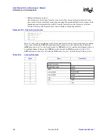
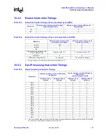
Page 164: ...tcomes Table 10 1 shows the branch latency penalty when these instructions are correctly predicted and when they are not A penalty of zero for correct prediction means that the core can execute the next instruction in the program flow in the cycle following the branch 10 3 Addressing Modes All load and store addressing modes implemented in the core do not add to the instruction latencies numbers T...

Page 165: ...Issue Latency without Branch Misprediction The minimum cycle distance from the issue clock of the current instruction to the first possible issue clock of the next instruction assuming best case conditions i e that the issuing of the next instruction is not stalled due to a resource dependency stall the next instruction is immediately available from the cache or memory interface the current instru...

Page 166: ...lculate Issue Latency and Result Latency for each instruction Looking at the issue column the UMLAL instruction starts to issue on cycle 0 and the next instruction ADD issues on cycle 2 so the Issue Latency for UMLAL is two From the code fragment there is a result dependency between the UMLAL instruction and the SUB instruction In Table 10 2 UMLAL starts to issue at cycle 0 and the SUB issues at c...

Page 167: ...e as Table 10 5 4 numbers in Table 10 5 LDR PC 2 8 LDM with PC in register list 3 numrega a numreg is the number of registers in the register list including the PC 10 max 0 numreg 3 Table 10 5 Data Processing Instruction Timings Mnemonic shifter operand is NOT a Shift Rotate by Register shifter operand is a Shift Rotate by Register OR shifter operand is RRX Minimum Issue Latency Minimum Result Lat...

Page 168: ...0x1FFFF 0 1 2 1 1 2 2 2 Rs 31 27 0x00 or Rs 31 27 0x1F 0 1 3 2 1 3 3 3 all others 0 1 4 3 1 4 4 4 SMLAL Rs 31 15 0x00000 or Rs 31 15 0x1FFFF 0 2 RdLo 2 RdHi 3 2 1 3 3 3 Rs 31 27 0x00 or Rs 31 27 0x1F 0 2 RdLo 3 RdHi 4 3 1 4 4 4 all others 0 2 RdLo 4 RdHi 5 4 1 5 5 5 SMLALxy N A N A 2 RdLo 2 RdHi 3 2 SMLAWy N A N A 1 3 2 SMLAxy N A N A 1 2 1 SMULL Rs 31 15 0x00000 or Rs 31 15 0x1FFFF 0 1 RdLo 2 RdH...

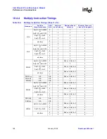
Page 169: ...y Minimum Result Latency Minimum Resource Latency Throughput MIA Rs 31 15 0x0000 or Rs 31 15 0xFFFF 1 1 1 Rs 31 27 0x0 or Rs 31 27 0xF 1 2 2 all others 1 3 3 MIAxy N A 1 1 1 MIAPH N A 1 2 2 Table 10 8 Implicit Accumulator Access Instruction Timings Mnemonic Minimum Issue Latency Minimum Result Latency Minimum Resource Latency Throughput MAR 2 2 2 MRA 1 RdLo 2 RdHi 3 a a If the next instruction nee...

Page 170: ...h 10 4 6 Status Register Access Instructions Table 10 9 Saturated Data Processing Instruction Timings Mnemonic Minimum Issue Latency Minimum Result Latency QADD 1 2 QSUB 1 2 QDADD 1 2 QDSUB 1 2 Table 10 10 Status Register Access Instruction Timings Mnemonic Minimum Issue Latency Minimum Result Latency MRS 1 2 MSR 2 6 if updating mode bits 1 ...

Page 171: ...f base LDRT 1 3 for load data 1 for writeback of base PLD 1 N A STR 1 1 for writeback of base STRB 1 1 for writeback of base STRBT 1 1 for writeback of base STRD 2 2 for writeback of base STRH 1 1 for writeback of base STRT 1 1 for writeback of base Table 10 12 Load and Store Multiple Instruction Timings Mnemonic Minimum Issue Latency Minimum Result Latency LDMa a See Table 10 4 for LDM timings wh...

Page 172: ...atency MRCa a MRC to R15 is unpredictable 4 4 MCR 2 N A Table 10 15 CP14 Register Access Instruction Timings Mnemonic Minimum Issue Latency Minimum Result Latency MRC 8 8 MRC to R15 9 9 MCR 8 N A LDC 11 N A STC 8 N A Table 10 16 Exception Generating Instruction Timings Mnemonic Minimum latency to first instruction of exception handler SWI 6 BKPT 6 UNDEFINED 6 Table 10 17 Count Leading Zeros Instru...

Page 173: ...Minimum Issue Latency with Branch Misprediction goes from 5 to 6 cycles This is due to the branch latency penalty see Table 10 1 If the equivalent ARM instruction maps to one in Table 10 4 the Minimum Issue Latency when the Branch is Taken increases by 1 cycle This is due to the branch latency penalty see Table 10 1 A Thumb BL instruction when H 0 will have the same timing as an ARM data processin...

Page 174: ...174 January 2004 Developer s Manual Intel XScale Core Developer s Manual Performance Considerations This Page Intentionally Left Blank ...

Page 175: ...rs however to obtain the maximum performance of your application code it should be optimized for the core using the techniques presented in this document A 1 1 About This Guide This guide considers that you are familiar with the ARM instruction set and the C language It consists of the following sections Section A 1 Introduction Outlines the contents of this guide Section A 2 The Intel XScale Core...

Page 176: ...ine 7 stages versus 5 stages which operates at a much higher frequency than its predecessors do This allows for greater overall performance The longer core pipeline has several negative consequences however Larger branch misprediction penalty 4 cycles in the core instead of 1 in StrongARM Architecture This is mitigated by dynamic branch prediction Larger load use delay LUD LUDs arise from load use...

Page 177: ...SC Superpipeline F1 F2 ID RF X1 X2 XWB M1 M2 Mx D1 D2 DWB Main execution pipeline MAC pipeline Memory pipeline Table A 1 Pipelines and Pipe stages Pipe Pipestage Description Covered In Main Execution Pipeline Handles data processing instructions Section A 2 3 IF1 IF2 Instruction Fetch ID Instruction Decode RF Register File Operand Shifter X1 ALU Execute X2 State Execute XWB Write back Memory Pipel...

Page 178: ... indicate that the operation has been completed and the result has been written back to the register file A 2 1 4 Register Scoreboarding In certain situations the pipeline may need to be stalled because of register dependencies between instructions A register dependency occurs when a previous MAC or load instruction is about to modify a register value that has not been returned to the register fil...

Page 179: ...ipestage to the RF pipestage The RF pipestage may issue a single instruction to either the X1 pipestage or the MAC unit multiply instructions go to the MAC while all others continue to X1 This means that M1 or X1 will be idle All load store instructions are routed to the memory pipeline after the effective addresses have been calculated in X1 The ARM V5TE bx branch and exchange instruction which i...

Page 180: ...BTB predicted the pipeline is flushed execution starts at the new target address and the branch s history is updated in the BTB Instruction Fetch Unit IFU The IFU is responsible for delivering instructions to the instruction decode ID pipestage One instruction word is delivered each cycle if possible to the ID The instruction could come from one of two sources instruction cache or fetch buffers A ...

Page 181: ...ands for data processing instructions as the shifter operand where a 32 bit shift can be performed before it is used as an input to the ALU This shifter is located in the second half of the RF pipestage A 2 3 4 X1 Execute Pipestages The X1 pipestage performs the following functions ALU calculation the ALU performs arithmetic and logic operations as required for data processing instructions and loa...

Page 182: ...resources for several cycles before a new instruction can be accepted The type of instruction and source arguments determines the number of cycles required No more than two instructions can occupy the MAC pipeline concurrently When the MAC is processing an instruction another instruction may not enter M1 unless the original instruction completes in the next cycle The MAC unit can operate on 16 bit...

Page 183: ...to set condition codes is Assume r0 contains the value a and r1 contains the value b add r0 r0 r1 cmp r0 0 However code can be optimized as follows making use of add instruction to set condition codes Assume r0 contains the value a and r1 contains the value b adds r0 r0 r1 The instructions that increment or decrement the loop counter can also be used to modify the condition codes This eliminates t...

Page 184: ...es to execute the else part and four cycles for the if part assuming best case conditions and no branch misprediction penalties In the case of the Intel XScale core a branch misprediction incurs a penalty of four cycles If the branch is mispredicted 50 of the time and if we consider that both the if part and the else part are equally likely to be taken on an average the code above takes 5 5 cycles...

Page 185: ... conditional instructions Consider the code sample shown below cmp r0 0 bne L1 add r0 r0 1 add r1 r1 1 add r2 r2 1 add r3 r3 1 add r4 r4 1 b L2 L1 sub r0 r0 1 sub r1 r1 1 sub r2 r2 1 sub r3 r3 1 sub r4 r4 1 L2 In the above code sample the cmp instruction takes 1 cycle to execute the if part takes 7 cycles to execute and the else part takes 6 cycles to execute If we were to change the code above so...

Page 186: ...ent int foo int a int b if a 0 b 0 return 0 else return 1 The optimized code for the if condition is cmp r0 0 cmpne r1 0 Similarly the code generated for the following C segment int foo int a int b if a 0 b 0 return 0 else return 1 is cmp r0 0 cmpeq r1 0 The use of conditional instructions in the above fashion improves performance by minimizing the number of branches thereby minimizing the penalti...

Page 187: ...field operations can be optimized as follows Set the bit number specified by r1 in register r0 mov r2 1 orr r0 r0 r2 asl r1 Clear the bit number specified by r1 in register r0 mov r2 1 bic r0 r0 r2 asl r1 Extract the bit value of the bit number specified by r1 of the value in r0 storing the value in r0 mov r1 r0 asr r1 and r0 r1 1 Extract the higher order 8 bits of the value in r0 storing the resu...

Page 188: ...DR instruction has the potential of incurring a cache miss in addition to polluting the data and instruction caches The code samples below illustrate cases when a combination of the above instructions can be used to set a register to a constant value Set the value of r0 to 127 mov r0 127 Set the value of r0 to 0xfffffefb mvn r0 260 Set the value of r0 to 257 mov r0 1 orr r0 r0 256 Set the value of...

Page 189: ... above optimization should only be used in cases where the multiply operation cannot be advanced far enough to prevent pipeline stalls Dividing an unsigned integer by an integer constant should be optimized to make use of the shift operation whenever possible Dividing r0 containing an unsigned value by an integer constant that can be represented as 2n mov r0 r0 LSR n Dividing a signed integer by a...

Page 190: ...f array operations can be optimized to make use of these addressing modes Set the contents of the word pointed to by r0 to the value contained in r1 and make r0 point to the next word str r1 r0 4 Increment the contents of r0 to make it point to the next word and set the contents of the word pointed to the value contained in r1 str r1 r0 4 Set the contents of the word pointed to by r0 to the value ...

Page 191: ... core is running much faster than external memory Executing non cached instructions severely curtails the processor s performance in this case and it is very important to do everything possible to minimize cache misses A 4 1 2 Round Robin Replacement Cache Policy Both the data and the instruction caches use a round robin replacement policy to evict a cache line The simple consequence of this is th...

Page 192: ... clock handlers OS critical code Time critical application code The disadvantage to locking code into the cache is that it reduces the cache size for the rest of the program How much code to lock is very application dependent and requires experimentation to optimize Code placed into the instruction cache should be aligned on a 1024 byte boundary and placed sequentially together as tightly as possi...

Page 193: ...s on what cache policy you are using for data objects A description of when to use a particular policy is described below The Intel XScale core allows dynamic modification of the cache policies at run time however the operation is requires considerable processing time and therefore should not be used by applications If the application is running under an OS then the OS may restrict you from using ...

Page 194: ...ocated to on chip RAM The following variables are good candidates for allocating to the on chip RAM Frequently used global data used for storing context for context switching Global variables that are accessed in time critical functions such as interrupt service routines The on chip RAM is created by locking a memory region into the Data cache see Section 6 4 Re configuring the Data Cache as Data ...

Page 195: ...ould be for caching the procedure call stack The stack can be allocated to the mini data cache so that it s use does not trash the main dcache This would keep local variables from global data Following are examples of data that could be assigned to mini dcache The stack space of a frequently occurring interrupt the stack is used only during the duration of the interrupt which is usually very small...

Page 196: ...t aligned to a cache line then the prefetch using the address of tdata i 1 ia may not include element id If the array was aligned on a cache line 12 bytes then the prefetch would halve to be placed on tdata i 1 id If the structure is not sized to a multiple of the cache line size then the prefetch address must be advanced appropriately and will require extra prefetch instructions Consider the foll...

Page 197: ...in a pool of memory known a literal pool These data blocks are located in the text or code address space so that they can be loaded using PC relative addressing However references to the literal pool area load the data into the data cache instead of the instruction cache Therefore it is possible that the literal may be present in both the data and instruction caches resulting in waste of space For...

Page 198: ... current memory components is often defined as 4k Memory lookup time or latency time for a selected page address is currently 2 to 3 bus clocks Thrashing occurs when subsequent memory accesses within the same memory bank access different pages The memory page change adds 3 to 4 bus clock cycles to memory latency This added delay extends the prefetch distance correspondingly making it more difficul...

Page 199: ...cessor will ignore the prefetch instruction the fault or table walk and continue processing the next instruction This is particularly advantageous in the case where a linked list or recursive data structure is terminated by a NULL pointer Prefetching the NULL pointer will not fault program flow A 4 4 1 Prefetch Distances Scheduling the prefetch instruction requires understanding the system latency...

Page 200: ...is write allocate along with a pending buffer A subsequent read to the same cache line does not require a new fill buffer but does require a pending buffer and a subsequent write will also require a new pending buffer A fill buffer is also allocated for each read to a non cached memory and a write buffer is needed for each memory write to non cached memory that is non coalescing Consequently a STM...

Page 201: ...to search and compare elements Similarly rearranging sections of data structures so that sections often written fit in the same half cache line 16 bytes for the core can reduce cache eviction write backs On a global scale techniques such as array merging can enhance the spatial locality of the data As an example of array merging consider the following code int a_array NMAX int b_array NMAX int ix ...

Page 202: ...e laid out as shown above assuming that the structure is aligned on a 32 byte boundary modifications to the Year2Date fields is likely to use two write buffers when the data is written out to memory However we can restrict the number of write buffers that are commonly used to 1 by rearranging the fields in the above data structure as shown below struct employee struct employee prev struct employee...

Page 203: ...isplace A i j from the cache Using blocking the code becomes for i 0 i 10000 i for j1 0 j 100 j for k1 0 k 100 k for j2 0 j 100 j for k2 0 k 100 k j j1 100 j2 k k1 100 k2 C j k A i k B j i A 4 4 9 Prefetch Unrolling When iterating through a loop data transfer latency can be hidden by prefetching ahead one or more iterations The solution incurs an unwanted side affect that the final interactions of...

Page 204: ...do_something p data p p next Recursive data structure traversal is another construct where prefetching can be applied This is similar to linked list traversal Consider the following pre order traversal of a binary tree preorder treeNode t if t process t data preorder t left preorder t right The pointer variable t becomes the pseudo induction variable in a recursive loop The data structures pointed...

Page 205: ...her This situation causes an increase in bus traffic when prefetching loop data In some cases where the loop mathematics are unaffected the problem can be resolved by induction variable interchange The above examples becomes for i 0 i NMAX i for j 0 j NMAX j prefetch A i j 1 sum A i j A 4 4 12 Loop Fusion Loop fusion is a process of combining multiple loops which reuse the same data in to one loop...

Page 206: ...eceiving register until the data can be used For example ldr r2 r0 Process code not yet cached latency 60 core clocks add r1 r1 r2 In the above case r2 is unavailable for processing until the add statement Prefetching the data load frees the register for use The example code becomes pld r0 prefetch the data keeping r2 available for use Process code ldr r2 r0 Process code ldr result latency is 3 co...

Page 207: ...the instructions surrounding the LDR instruction should be rearranged to avoid this stall Consider the following example add r1 r2 r3 ldr r0 r5 add r6 r0 r1 sub r8 r2 r3 mul r9 r2 r3 In the code shown above the ADD instruction following the LDR would stall for 2 cycles because it uses the result of the load The code can be rearranged as follows to prevent the stalls ldr r0 r5 add r1 r2 r3 sub r8 r...

Page 208: ...er this In the code sample above the ADD and the LDR instruction can be moved before the MOV instruction Note that this would prevent pipeline stalls if the load hits the data cache However if the load is likely to miss the data cache move the LDR instruction so that it executes as early as possible before the SUB instruction However moving the LDR instruction before the SUB instruction would chan...

Page 209: ...ed sequentially should not exceed 4 Also note that a preload instruction may cause a fill buffer to be used As a result the number of preload instructions outstanding should also be considered to arrive at the number of loads that are outstanding Similarly the number of write buffers also limits the number of successive writes that can be issued before the processor stalls No more than eight store...

Page 210: ...M which issues in four clock cycles Avoid LDRDs targeting R12 this incurs an extra cycle of issue latency The LDRD instruction has a result latency of 3 or 4 cycles depending on the destination register being accessed assuming the data being loaded is in the data cache add r6 r7 r8 sub r5 r6 r9 The following ldrd instruction would load values into registers r0 and r1 ldrd r0 r3 orr r8 r1 0xf mul r...

Page 211: ...d on an 8 byte boundary This can be achieved using the LDM instructions as shown below r0 contains the address of the value being copied r1 contains the address of the destination location ldm r0 r2 r3 ldm r1 r4 r5 adds r0 r2 r4 adc r1 r3 r5 If the code were written as shown above assuming all the accesses hit the cache the code would take 11 cycles to complete Rewriting the code as shown below us...

Page 212: ...SL 2 The code above can be rearranged as follows to remove the 1 cycle stall add r1 r2 r3 sub r6 r7 r8 mov r4 r1 LSL 2 All data processing instructions incur a 2 cycle issue penalty and a 2 cycle result penalty when the shifter operand is a shift rotate by a register or shifter operand is RRX Since the next instruction would always incur a 2 cycle issue penalty there is no way to avoid such a stal...

Page 213: ...1 r2 mov r4 r0 Note that a multiply instruction that sets the condition codes blocks the whole pipeline A 4 cycle multiply operation that sets the condition codes behaves the same as a 4 cycle issue operation Consider the following code segment muls r0 r1 r2 add r3 r3 1 sub r4 r4 1 sub r5 r5 1 The add operation above would stall for 3 cycles if the multiply takes 4 cycles to complete It is better ...

Page 214: ...ould stall for 4 cycles SWP and SWPB instructions should therefore be used only where absolutely needed For example the following code may be used to swap the contents of 2 memory locations Swap the contents of memory locations pointed to by r0 and r1 ldr r2 r0 swp r2 r1 str r2 r1 The code above takes 9 cycles to complete The rewritten code below takes 6 cycles to execute Swap the contents of memo...

Page 215: ... The code can be rearranged as shown below to prevent this stall mra r6 r7 acc0 add r1 r1 1 mra r8 r9 acc0 Similarly the code shown below would incur a 2 cycle penalty due to the 3 cycle result latency for the second destination register mra r6 r7 acc0 mov r1 r7 mov r0 r6 add r2 r2 1 The stalls incurred by the code shown above can be prevented by rearranging the code mra r6 r7 acc0 add r2 r2 1 mov...

Page 216: ...ider the following code sample mia acc0 r2 r3 mra r4 r5 acc0 The MRA instruction above can stall from 0 to 2 cycles depending on the values in the registers r2 and r3 due to the 1 to 3 cycle result latency The MIAPH instruction has an issue latency of 1 cycle result latency of 2 cycles and a resource latency of 2 cycles Consider the code sample shown below add r1 r2 r3 miaph acc0 r3 r4 miaph acc0 ...

Page 217: ... 2 cycle result latency of the MRS instruction In the code example above the ADD instruction can be moved before the ORR instruction to prevent this stall A 5 8 Scheduling CP15 Coprocessor Instructions The MRC instruction has an issue latency of 1 cycle and a result latency of 3 cycles The MCR instruction has an issue latency of 1 cycle Consider the code sample add r1 r2 r3 mrc p15 0 r7 C1 C0 0 mo...

Page 218: ...rformance Trade Off Many optimizations mentioned in the previous chapters improve the performance of ARM code However using these instructions will result in increased code size Use the following optimizations to reduce the space requirements of the application code A 7 1 1 Multiple Word Load and Store The LDM STM instructions are one word long and let you load or store multiple registers at once ...

Page 219: ... bit instruction register and test data registers to support software debug The size of the instruction register depends on which variant of the Intel XScale core is being used This can be found out by examining the CoreGen field of Coprocessor 15 ID Register bits 15 13 See Table 7 4 ID Register on page 7 81 for more details A CoreGen value of 0x1 means the JTAG instruction register size is 5 bits...

Page 220: ...220 January 2004 Developer s Manual Intel XScale Core Developer s Manual Test Features This Page Intentionally Left Blank ...

Reviews: