background image

Datasheet

91

Thermal Specifications and Design Considerations

NOTES:
1.

Intel does not support or recommend operation of the thermal diode under reverse bias.

2.

Same as I

FW 

in 

Table 33

.

3.

Characterized across a temperature range of 50–80 °C.

4.

Not 100% tested. Specified by design characterization.

5.

The ideality factor, nQ, represents the deviation from ideal transistor model behavior as 
exemplified by the equation for the collector current:

I

C

 = I

S

 * (e 

qV

BE

/n

Q

kT

 –1)

Where I

S

 = saturation current, q = electronic charge, V

BE

 = voltage across the transistor 

base emitter junction (same nodes as VD), k = Boltzmann Constant, and T = absolute 

temperature (Kelvin).

6.

The series resistance, R

T,

 provided in the Diode Model Table (

Table 33

) can be used for 

more accurate readings as needed. 

The processor does not support the diode correction offset that exists on other Intel 

processors

Table 34.

Thermal “Diode” Parameters using Transistor Model

Symbol

Parameter

Min

Typ

Max

Unit

Notes

I

FW

Forward Bias Current

5

200

µA

1, 2

I

E

Emitter Current

5

200

µA

n

Q

Transistor Ideality

0.997

1.001

1.005

-

3, 4, 5

Beta

0.391

0.760

3, 4

R

T

Series Resistance

2.79

4.52

6.24

Ω

3, 6

Table 35.

Thermal Diode Interface

Signal Name

Land Number

Signal 

Description

THERMDA

AL1

diode anode

THERMDC

AK1

diode cathode

Summary of Contents for CORE 2 DUO E4000 - 3-2008

Page 1: ...xtreme Processor X6800Δ and Intel Core 2 Duo Desktop Processor E6000Δ and E4000Δ Sequences Datasheet on 65 nm Process in the 775 land LGA Package and supporting Intel 64 Architecture and supporting Intel Virtualization Technology October 2007 ...

Page 2: ... software configurations See http www intel com technology intel64 index htm for more information including details on which processors support Intel 64 or consult with your system vendor for more information No computer system can provide absolute security under all conditions Intel Trusted Execution Technology Intel TXT is a security technology under development by Intel and requires for operati...

Page 3: ...d Processor Clocking 31 2 7 6 FSB Frequency Select Signals BSEL 2 0 31 2 7 7 Phase Lock Loop PLL and Filter 32 2 7 8 BCLK 1 0 Specifications CK505 based Platforms 32 2 7 9 BCLK 1 0 Specifications CK410 based Platforms 34 2 8 PECI DC Specifications 35 3 Package Mechanical Specifications 37 3 1 Package Mechanical Drawing 37 3 1 1 Processor Component Keep Out Zones 41 3 1 2 Package Loading Specificat...

Page 4: ...sor Specifications 101 7 1 Mechanical Specifications 102 7 1 1 Boxed Processor Cooling Solution Dimensions 102 7 1 2 Boxed Processor Fan Heatsink Weight 103 7 1 3 Boxed Processor Retention Mechanism and Heatsink Attach Clip Assembly 103 7 2 Electrical Requirements 103 7 2 1 Fan Heatsink Power Supply 103 7 3 Thermal Specifications 105 7 3 1 Boxed Processor Cooling Requirements 105 7 3 2 Fan Speed C...

Page 5: ... Profile Intel Core 2 Duo Desktop Processor E4500 and E4600 with 2 MB L2 Cache 83 23 Thermal Profile Intel Core Duo Desktop Processor E6000 and E4000 Sequence with 2 MB L2 Cache 84 24 Thermal Profile Intel Core 2 Extreme Processor X6800 85 25 Case Temperature TC Measurement Location 86 26 Thermal Monitor 2 Frequency and Voltage Ordering 88 27 Processor PECI Topology 92 28 Conceptual Fan Control on...

Page 6: ...ssor Loading Specifications 41 22 Package Handling Guidelines 41 23 Processor Materials 42 24 Alphabetical Land Assignments 50 25 Numerical Land Assignment 60 26 Signal Description Sheet 1 of 9 70 27 Processor Thermal Specifications 80 28 Thermal Profile Intel Core 2 Duo Desktop Processor E6x50 Sequence and E6540 with 4 MB L2 Cache 81 29 Thermal Profile Intel Core Duo Desktop Processor E6000 Seque...

Page 7: ...ion 7 3 2 Fan Speed Control Operation Intel Core2 Extreme Processor X6800 Only and Section 7 3 3 Fan Speed Control Operation Intel Core2 Duo Desktop Processor E6000 and E4000 Sequences Only January 2007 004 Added Intel Core 2 Duo Desktop Processor E6420 E6320 and E4400 information April 2007 005 Added Intel Core 2 Duo Desktop Processor E6850 E6750 E6550 E6540 and E4500 information Added specificat...

Page 8: ...8 Datasheet ...

Page 9: ...cessor X6800 only Available at 3 00 GHz 2 66 GHz 2 40 GHz 2 33 GHz 2 13 GHz and 1 86 GHz Intel Core 2 Duo desktop processor E6850 E6750 E6700 E6600 E6540 E6540 E6420 E6400 E6320 and E6300 only Available at 2 40 GHz 2 20 GHz 2 00 GHz and 1 80 GHz and Intel Core 2 Duo desktop processor E4600 E4500 E4400 and E4300 only Enhanced Intel SpeedStep Technology Supports Intel 64 architecture Supports Intel ...

Page 10: ...10 Datasheet ...

Page 11: ...ors support several Advanced Technologies including the Execute Disable Bit Intel 64 architecture and Enhanced Intel SpeedStep Technology The Intel Core 2 Duo desktop processor E6000 sequence and Intel Core 2 Extreme processor X6800 support Intel Virtualization Technology Intel VT In addition the Intel Core 2 Duo desktop processors E6850 E6750 and E6550 support Intel Trusted Execution Technology I...

Page 12: ...he Intel Core 2 Extreme processor X6800 The processor is a single package that contains one or more execution units Keep out zone The area on or near the processor that system design can not use Processor core Processor core die with integrated L2 cache LGA775 socket The processors mate with the system board through a surface mount 775 land LGA socket Integrated heat spreader IHS A component of th...

Page 13: ...nce and power consumptions based on processor utilization This may lower average power consumption in conjunction with OS support Intel Virtualization Technology Intel VT Intel Virtualization Technology provides silicon based functionality that works together with compatible Virtual Machine Monitor VMM software to improve upon software only solutions Because this virtualization hardware provides a...

Page 14: ... com design pentiumXE designex 306830 htm Balanced Technology Extended BTX System Design Guide www formfactors org Voltage Regulator Down VRD 11 0 Processor Power Delivery Design Guidelines For Desktop LGA775 Socket http www intel com design processor applnots 313214 htm LGA775 Socket Mechanical Design Guide http intel com design Pentium4 guides 302666 htm Intel Virtualization Technology Specifica...

Page 15: ...ming out of an idle condition Similarly they act as a storage well for current when entering an idle condition from a running condition The motherboard must be designed to ensure that the voltage provided to the processor remains within the specifications listed in Table 5 Failure to do so can result in timing violations or reduced lifetime of the component 2 2 1 VCC Decoupling VCC regulator solut...

Page 16: ...2 Enhanced Intel SpeedStep Technology or Extended HALT State The processor uses six voltage identification signals VID 6 1 to support automatic selection of power supply voltages Table 2 specifies the voltage level corresponding to the state of VID 6 1 A 1 in this table refers to a high voltage level and a 0 refers to a low voltage level If the processor socket is empty VID 6 1 111111 or the volta...

Page 17: ... 1 3625 1 1 0 0 1 0 0 9875 0 1 0 0 1 1 1 3750 1 1 0 0 0 1 1 0000 0 1 0 0 1 0 1 3875 1 1 0 0 0 0 1 0125 0 1 0 0 0 1 1 4000 1 0 1 1 1 1 1 0250 0 1 0 0 0 0 1 4125 1 0 1 1 1 0 1 0375 0 0 1 1 1 1 1 4250 1 0 1 1 0 1 1 0500 0 0 1 1 1 0 1 4375 1 0 1 1 0 0 1 0625 0 0 1 1 0 1 1 4500 1 0 1 0 1 1 1 0750 0 0 1 1 0 0 1 4625 1 0 1 0 1 0 1 0875 0 0 1 0 1 1 1 4750 1 0 1 0 0 1 1 1000 0 0 1 0 1 0 1 4875 1 0 1 0 0 0 ...

Page 18: ...er or ground When tying any signal to power or ground a resistor will also allow for system testability Resistor values should be within 20 of the impedance of the motherboard trace for front side bus signals For unused GTL input or I O signals use pull up resistors of the same value as the on die termination resistors RTT For details see Table 15 TAP and CMOS signals do not include on die termina...

Page 19: ...aximum and minimum ratings only and lie outside the functional limits of the processor Within functional operation limits functionality and long term reliability can be expected At conditions outside functional operation condition limits but within absolute maximum and minimum ratings neither functionality nor long term reliability can be expected If a device is returned to conditions within funct...

Page 20: ... within these limits will not affect the long term reliability of the device For functional operation refer to the processor case temperature specifications 4 This rating applies to the processor and does not include any tray or packaging 5 Failure to adhere to this specification can affect the long term reliability of the processor Table 5 Voltage and Current Specifications Symbol Parameter Min T...

Page 21: ...rocessor during a power management event Thermal Monitor 2 Enhanced Intel SpeedStep Technology or Extended HALT State 4 These voltages are targets only A variable voltage source should exist on systems in the event that a different voltage is required See Section 2 3 and Table 2 for more information 5 The voltage specification requirements are measured across VCC_SENSE and VSS_SENSE lands at the s...

Page 22: ...s must be taken from processor VCC and VSS lands Refer to the Voltage Regulator Down VRD 11 0 Processor Power Delivery Design Guidelines For Desktop LGA775 Socket for socket loadline guidelines and VR implementation details 4 Adherence to this loadline specification is required to ensure reliable processor operation Maximum Voltage 1 30 mΩ Typical Voltage 1 425 mΩ Minimum Voltage 1 55 mΩ 0 0 000 0...

Page 23: ...tion feedback for voltage regulator circuits must be taken from processor VCC and VSS lands Refer to the Voltage Regulator Down VRD 11 0 Processor Power Delivery Design Guidelines For Desktop LGA775 Socket for socket loadline guidelines and VR implementation details Figure 1 VCC Static and Transient Tolerance for Processors with 4 MB L2 Cache VID 0 000 VID 0 013 VID 0 025 VID 0 038 VID 0 050 VID 0...

Page 24: ...ts must be taken from processor VCC and VSS lands Refer to the Voltage Regulator Down VRD 11 0 Processor Power Delivery Design Guidelines For Desktop LGA775 Socket for socket loadline guidelines and VR implementation details 4 Adherence to this loadline specification is required to ensure reliable processor operation Maximum Voltage 1 40 mΩ Typical Voltage 1 53 mΩ Minimum Voltage 1 65 mΩ 0 0 000 0...

Page 25: ...ng from a high to low current load condition This overshoot cannot exceed VID VOS_MAX VOS_MAX is the maximum allowable overshoot voltage The time duration of the overshoot event must not exceed TOS_MAX TOS_MAX is the maximum allowable time duration above VID These specifications apply to the processor die voltage as measured across the VCC_SENSE and VSS_SENSE lands Figure 2 VCC Static and Transien...

Page 26: ...tforms implement separate power planes for each processor and chipset separate VCC and VTT supplies are necessary This configuration allows for improved noise tolerance as processor frequency increases Speed enhancements to data and address busses have caused signal integrity considerations and platform design methods to become even more critical than with previous processor families The GTL input...

Page 27: ...nted on the system board these signals are used to support a debug port interposer In systems with the debug port implemented on the system board these signals are no connects 3 The value of these signals during the active to inactive edge of RESET defines the processor configuration options See Section 6 1 for details 4 PROCHOT signal type is open drain output and CMOS input Table 9 FSB Signal Gr...

Page 28: ...DEFER DRDY DSTBN 3 0 DSTBP 3 0 HIT HITM LOCK PROCHOT REQ 4 0 RS 2 0 TRDY A20M BCLK 1 0 BSEL 2 0 COMP 8 3 0 IGNNE INIT ITP_CLK 1 0 LINT0 INTR LINT1 NMI PWRGOOD RESET SMI STPCLK TESTHI 13 0 VID 6 1 GTLREF 1 0 TCK TDI TMS TRST VTT_SEL MSID 1 0 Open Drain Signals1 NOTES 1 Signals that do not have RTT nor are actively driven to their high voltage level THERMTRIP FERR PBE IERR BPM 5 0 BR0 TDO FCx Table ...

Page 29: ...4 VIH is defined as the voltage range at a receiving agent that will be interpreted as a logical high value 5 VIH and VOH may experience excursions above VTT VOH Output High Voltage VTT 0 10 VTT V 5 3 IOL Output Low Current N A VTT_MAX RTT_MIN 2 RON_MIN A ILI Input Leakage Current N A 100 µA 6 6 Leakage to VSS with land held at VTT ILO Output Leakage Current N A 100 µA 7 7 Leakage to VTT with land...

Page 30: ... high value 5 VIH and VOH may experience excursions above VTT VOL Output Low Voltage 0 10 VTT 0 10 V 3 VOH Output High Voltage 0 90 VTT VTT 0 10 V 3 6 5 6 All outputs are open drain IOL Output Low Current 1 70 4 70 mA 3 7 7 IOL is measured at 0 10 VTT IOH is measured at 0 90 VTT IOH Output High Current 1 70 4 70 mA 3 7 ILI Input Leakage Current N A 100 µA 8 8 Leakage to VSS with land held at VTT I...

Page 31: ... The required frequency is determined by the processor chipset and clock synthesizer All agents must operate at the same frequency The Intel Core2 Duo desktop processors E6850 E6750 E6550 and E6540 operate at 1333 MHz selected by the 333 MHz BCLK 2 0 frequency The Intel Core2 Duo desktop processors E6700 E6600 E6420 E6400 E6320 and E6300 operate at 1066 MHz selected by the 266 MHz BCLK 2 0 frequen...

Page 32: ...luding overshoot or undershoot VH Input High Voltage N A N A 1 15 V 4 2 VCROSS abs Absolute Crossing Point 0 300 N A 0 550 V 4 5 3 4 5 3 Crossing voltage is defined as the instantaneous voltage value when the rising edge of BCLK0 equals the falling edge of BCLK1 4 VHavg is the statistical average of the VH measured by the oscilloscope 5 The crossing point must meet the absolute and relative crossi...

Page 33: ...SS CLK 1 CLK 0 Low Time VCROSS Min 300 mV VCROSS Max 550 mV median VCROSS median VCROSS Median 75 mV Median 75 mV VCROSS 660 670 680 690 700 710 720 730 740 750 760 770 780 790 800 810 820 830 840 850 200 250 300 350 400 450 500 550 600 650 VHavg mV Crossing Point mV 550 mV 300 mV 300 0 5 VHavg 700 550 0 5 VHavg 700 150 mV 150 mV 0 0V 0 0V Slew_rise 150mV 150mV V_swing Slew _fall Diff ...

Page 34: ...illoscope 5 VHavg can be measured directly using Vtop on Agilent oscilloscopes and High on Tektronix oscilloscopes ΔVCROSS Range of Crossing Points N A N A 0 140 V 4 5 VOS Overshoot N A N A VH 0 3 V 4 6 6 Overshoot is defined as the absolute value of the maximum voltage VUS Undershoot 0 300 N A N A V 4 7 7 Undershoot is defined as the absolute value of the minimum voltage VRBM Ringback Margin 0 20...

Page 35: ...C Electrical Limits Symbol Definition and Conditions Min Max Units Notes1 NOTES 1 VTT supplies the PECI interface PECI behavior does not affect VTT min max specifications Refer to Table 4 for VTT specifications Vin Input Voltage Range 0 15 VTT V Vhysteresis Hysteresis 0 1 VTT V 2 2 The input buffers use a Schmitt triggered input design for improved noise immunity Vn Negative edge threshold voltage...

Page 36: ...Electrical Specifications 36 Datasheet ...

Page 37: ...rated Heat Spreader IHS Thermal Interface Material TIM Processor core die Package substrate Capacitors NOTE 1 Socket and System Board are included for reference and are not part of processor package 3 1 Package Mechanical Drawing The package mechanical drawings are shown in Figure 9 and Figure 10 The drawings include dimensions necessary to design a thermal solution for the processor These dimensi...

Page 38: ...Package Mechanical Specifications 38 Datasheet Figure 9 Processor Package Drawing Sheet 1 of 3 ...

Page 39: ...Datasheet 39 Package Mechanical Specifications Figure 10 Processor Package Drawing Sheet 2 of 3 ...

Page 40: ...Package Mechanical Specifications 40 Datasheet Figure 11 Processor Package Drawing Sheet 3 of 3 ...

Page 41: ...ge handling in terms of recommended maximum loading on the processor IHS relative to a fixed substrate These package handling loads may be experienced during heatsink removal Table 21 Processor Loading Specifications Parameter Minimum Maximum Notes Static 80 N 17 lbf 311 N 70 lbf 1 2 3 NOTES 1 These specifications apply to uniform compressive loading in a direction normal to the processor IHS 2 Th...

Page 42: ... Processor Materials Table 23 lists some of the package components and associated materials 3 1 7 Processor Markings Figure 12 through Figure 16show the topside markings on the processor The diagrams are to aid in the identification of the processor Table 23 Processor Materials Component Material Integrated Heat Spreader IHS Nickel Plated Copper Substrate Fiber Reinforced Resin Substrate Lands Gol...

Page 43: ...ors E6000 Sequence with 4 MB L2 Cache with 1066 MHz FSB Figure 14 Processor Top Side Markings Example for the Intel Core 2 Duo Desktop Processors E6000 Sequence with 2 MB L2 Cache ATPO S N INTEL 05 INTEL CORE 2 DUO 6700 SLxxx COO 2 66GHZ 4M 1066 06 FPO M e4 ATPO S N INTEL 05 INTEL CORE 2 DUO 6400 SLxxx COO 2 13GHZ 2M 1066 06 FPO M e4 ...

Page 44: ...el Core 2 Duo Desktop Processors E4000 Sequence with 2 MB L2 Cache ATPO S N INTEL 05 E4500 INTEL CORE 2 DUO SLxxx COO 2 20GHZ 2M 800 06 FPO M e4 Figure 16 Processor Top Side Markings for the Intel Core 2 Extreme Processor X6800 ATPO S N INTEL 05 INTEL CORE 2 EXTREME 6800 SLxxx COO 2 93GHZ 4M 1066 05B FPO M e4 ...

Page 45: ...nd Coordinates and Quadrants Top View 1 2 3 4 5 6 7 8 9 10 11 12 13 14 15 16 17 18 19 20 21 22 23 24 25 26 27 28 29 30 A B C D E F G H J K L M N P R T U V W Y AA AB AC AD AE AF AG AH AJ AK AL AM AN A B C D E F G H J K L M N P R T U V W Y AA AB AC AD AE AF AG AH AJ AK AL AM AN 1 2 3 4 5 6 7 8 9 10 11 12 13 14 15 16 17 18 19 20 21 22 23 24 25 26 27 28 29 30 Preliminary Socket 775 Quadrants Top View ...

Page 46: ...Package Mechanical Specifications 46 Datasheet ...

Page 47: ...ains the land listings for the processor The land out footprint is shown in Figure 18 and Figure 19 These figures represent the land out arranged by land number and they show the physical location of each signal on the package land array top view Table 24 provides a listing of all processor lands ordered alphabetically by land signal name Table 25 provides a listing of all processor lands ordered ...

Page 48: ...Y VCC VCC VCC VCC VCC VCC VCC VCC W VCC VCC VCC VCC VCC VCC VCC VCC V VSS VSS VSS VSS VSS VSS VSS VSS U VCC VCC VCC VCC VCC VCC VCC VCC T VCC VCC VCC VCC VCC VCC VCC VCC R VSS VSS VSS VSS VSS VSS VSS VSS P VSS VSS VSS VSS VSS VSS VSS VSS N VCC VCC VCC VCC VCC VCC VCC VCC M VCC VCC VCC VCC VCC VCC VCC VCC L VSS VSS VSS VSS VSS VSS VSS VSS K VCC VCC VCC VCC VCC VCC VCC VCC J VCC VCC VCC VCC VCC VCC ...

Page 49: ...3 A21 VSS FC39 VTT_OUT_ RIGHT AA VCC VSS A19 VSS A20 FC17 VSS FC0 Y VCC VSS A18 A16 VSS TESTHI1 TESTHI12 FC44 MSID0 W VCC VSS VSS A14 A15 VSS RSVD MSID1 V VCC VSS A10 A12 A13 FC30 FC29 FC28 U VCC VSS VSS A9 A11 VSS FC4 COMP1 T VCC VSS ADSTB0 VSS A8 FERR PBE VSS COMP3 R VCC VSS A4 RSVD VSS INIT SMI TESTHI11 P VCC VSS VSS RSVD RSVD VSS IGNNE PWRGOOD N VCC VSS REQ2 A5 A7 STPCLK THERMTRIP VSS M VCC VS...

Page 50: ...n Clock Input Output ADSTB0 R6 Source Synch Input Output ADSTB1 AD5 Source Synch Input Output BCLK0 F28 Clock Input BCLK1 G28 Clock Input BNR C2 Common Clock Input Output BPM0 AJ2 Common Clock Input Output BPM1 AJ1 Common Clock Input Output BPM2 AD2 Common Clock Input Output BPM3 AG2 Common Clock Input Output BPM4 AF2 Common Clock Input Output BPM5 AG3 Common Clock Input Output BPRI G8 Common Cloc...

Page 51: ...utput D56 A17 Source Synch Input Output D57 B18 Source Synch Input Output D58 C21 Source Synch Input Output D59 B21 Source Synch Input Output D60 B19 Source Synch Input Output Table 24 Alphabetical Land Assignments Land Name Land Signal Buffer Type Direction D61 A19 Source Synch Input Output D62 A22 Source Synch Input Output D63 B22 Source Synch Input Output DBI0 A8 Source Synch Input Output DBI1 ...

Page 52: ...ERVED AC4 RESERVED AE4 RESERVED AE6 RESERVED AH2 RESERVED D1 RESERVED D14 Table 24 Alphabetical Land Assignments Land Name Land Signal Buffer Type Direction RESERVED D16 RESERVED E23 RESERVED E6 RESERVED E7 RESERVED F23 RESERVED F29 RESERVED G6 RESERVED N4 RESERVED N5 RESERVED P5 RESERVED V2 RESET G23 Common Clock Input RS0 B3 Common Clock Input RS1 F5 Common Clock Input RS2 A3 Common Clock Input ...

Page 53: ...her VCC AF19 Power Other VCC AF21 Power Other Table 24 Alphabetical Land Assignments Land Name Land Signal Buffer Type Direction VCC AF22 Power Other VCC AF8 Power Other VCC AF9 Power Other VCC AG11 Power Other VCC AG12 Power Other VCC AG14 Power Other VCC AG15 Power Other VCC AG18 Power Other VCC AG19 Power Other VCC AG21 Power Other VCC AG22 Power Other VCC AG25 Power Other VCC AG26 Power Other ...

Page 54: ...r Other VCC AM15 Power Other VCC AM18 Power Other Table 24 Alphabetical Land Assignments Land Name Land Signal Buffer Type Direction VCC AM19 Power Other VCC AM21 Power Other VCC AM22 Power Other VCC AM25 Power Other VCC AM26 Power Other VCC AM29 Power Other VCC AM30 Power Other VCC AM8 Power Other VCC AM9 Power Other VCC AN11 Power Other VCC AN12 Power Other VCC AN14 Power Other VCC AN15 Power Ot...

Page 55: ... Power Other Table 24 Alphabetical Land Assignments Land Name Land Signal Buffer Type Direction VCC T27 Power Other VCC T28 Power Other VCC T29 Power Other VCC T30 Power Other VCC T8 Power Other VCC U23 Power Other VCC U24 Power Other VCC U25 Power Other VCC U26 Power Other VCC U27 Power Other VCC U28 Power Other VCC U29 Power Other VCC U30 Power Other VCC U8 Power Other VCC V8 Power Other VCC W23...

Page 56: ...r Other VSS AB7 Power Other VSS AC3 Power Other VSS AC6 Power Other Table 24 Alphabetical Land Assignments Land Name Land Signal Buffer Type Direction VSS AC7 Power Other VSS AD4 Power Other VSS AD7 Power Other VSS AE10 Power Other VSS AE13 Power Other VSS AE16 Power Other VSS AE17 Power Other VSS AE2 Power Other VSS AE20 Power Other VSS AE24 Power Other VSS AE25 Power Other VSS AE26 Power Other V...

Page 57: ...her VSS AK29 Power Other VSS AK30 Power Other Table 24 Alphabetical Land Assignments Land Name Land Signal Buffer Type Direction VSS AK5 Power Other VSS AK7 Power Other VSS AL10 Power Other VSS AL13 Power Other VSS AL16 Power Other VSS AL17 Power Other VSS AL20 Power Other VSS AL23 Power Other VSS AL24 Power Other VSS AL27 Power Other VSS AL28 Power Other VSS AL7 Power Other VSS AM1 Power Other VS...

Page 58: ...ther VSS H10 Power Other VSS H11 Power Other Table 24 Alphabetical Land Assignments Land Name Land Signal Buffer Type Direction VSS H12 Power Other VSS H13 Power Other VSS H14 Power Other VSS H17 Power Other VSS H18 Power Other VSS H19 Power Other VSS H20 Power Other VSS H21 Power Other VSS H22 Power Other VSS H23 Power Other VSS H24 Power Other VSS H25 Power Other VSS H26 Power Other VSS H27 Powe...

Page 59: ...wer Other VSS V7 Power Other VSS W4 Power Other Table 24 Alphabetical Land Assignments Land Name Land Signal Buffer Type Direction VSS W7 Power Other VSS Y2 Power Other VSS Y5 Power Other VSS Y7 Power Other VSS_MB_ REGULATION AN6 Power Other Output VSS_SENSE AN4 Power Other Output VSSA B23 Power Other VTT A25 Power Other VTT A26 Power Other VTT A27 Power Other VTT A28 Power Other VTT A29 Power Oth...

Page 60: ...rce Synch Input Output B8 VSS Power Other B9 DSTBP0 Source Synch Input Output B10 D10 Source Synch Input Output B11 VSS Power Other B12 D13 Source Synch Input Output B13 COMP8 Power Other Input B14 VSS Power Other B15 D53 Source Synch Input Output B16 D55 Source Synch Input Output B17 VSS Power Other B18 D57 Source Synch Input Output B19 D60 Source Synch Input Output B20 VSS Power Other B21 D59 So...

Page 61: ... VTT Power Other D28 VTT Power Other Table 25 Numerical Land Assignment Land Land Name Signal Buffer Type Direction D29 VTT Power Other D30 VTT Power Other E2 VSS Power Other E3 TRDY Common Clock Input E4 HITM Common Clock Input Output E5 FC20 Power Other E6 RESERVED E7 RESERVED E8 VSS Power Other E9 D19 Source Synch Input Output E10 D21 Source Synch Input Output E11 VSS Power Other E12 DSTBP1 Sou...

Page 62: ...urce Synch Input Output G17 D36 Source Synch Input Output G18 D35 Source Synch Input Output G19 DSTBP2 Source Synch Input Output G20 DSTBN2 Source Synch Input Output Table 25 Numerical Land Assignment Land Land Name Signal Buffer Type Direction G21 D44 Source Synch Input Output G22 D47 Source Synch Input Output G23 RESET Common Clock Input G24 TESTHI6 Power Other Input G25 TESTHI3 Power Other Inpu...

Page 63: ...put K7 VSS Power Other K8 VCC Power Other Table 25 Numerical Land Assignment Land Land Name Signal Buffer Type Direction K23 VCC Power Other K24 VCC Power Other K25 VCC Power Other K26 VCC Power Other K27 VCC Power Other K28 VCC Power Other K29 VCC Power Other K30 VCC Power Other L1 LINT1 Asynch CMOS Input L2 TESTHI13 Power Other Input L3 VSS Power Other L4 A06 Source Synch Input Output L5 A03 Sou...

Page 64: ...Power Other R6 ADSTB0 Source Synch Input Output Table 25 Numerical Land Assignment Land Land Name Signal Buffer Type Direction R7 VSS Power Other R8 VCC Power Other R23 VSS Power Other R24 VSS Power Other R25 VSS Power Other R26 VSS Power Other R27 VSS Power Other R28 VSS Power Other R29 VSS Power Other R30 VSS Power Other T1 COMP1 Power Other Input T2 FC4 Power Other T3 VSS Power Other T4 A11 Sou...

Page 65: ...4 A20 Source Synch Input Output Table 25 Numerical Land Assignment Land Land Name Signal Buffer Type Direction Y5 VSS Power Other Y6 A19 Source Synch Input Output Y7 VSS Power Other Y8 VCC Power Other Y23 VCC Power Other Y24 VCC Power Other Y25 VCC Power Other Y26 VCC Power Other Y27 VCC Power Other Y28 VCC Power Other Y29 VCC Power Other Y30 VCC Power Other AA1 VTT_OUT_RIGHT Power Other Output AA...

Page 66: ...VCC Power Other AE1 TCK TAP Input AE2 VSS Power Other Table 25 Numerical Land Assignment Land Land Name Signal Buffer Type Direction AE3 FC18 Power Other AE4 RESERVED AE5 VSS Power Other AE6 RESERVED AE7 VSS Power Other AE8 SKTOCC Power Other Output AE9 VCC Power Other AE10 VSS Power Other AE11 VCC Power Other AE12 VCC Power Other AE13 VSS Power Other AE14 VCC Power Other AE15 VCC Power Other AE16...

Page 67: ...er Other AG18 VCC Power Other AG19 VCC Power Other AG20 VSS Power Other Table 25 Numerical Land Assignment Land Land Name Signal Buffer Type Direction AG21 VCC Power Other AG22 VCC Power Other AG23 VSS Power Other AG24 VSS Power Other AG25 VCC Power Other AG26 VCC Power Other AG27 VCC Power Other AG28 VCC Power Other AG29 VCC Power Other AG30 VCC Power Other AH1 VSS Power Other AH2 RESERVED AH3 VS...

Page 68: ...6 FC8 Power Other AK7 VSS Power Other AK8 VCC Power Other Table 25 Numerical Land Assignment Land Land Name Signal Buffer Type Direction AK9 VCC Power Other AK10 VSS Power Other AK11 VCC Power Other AK12 VCC Power Other AK13 VSS Power Other AK14 VCC Power Other AK15 VCC Power Other AK16 VSS Power Other AK17 VSS Power Other AK18 VCC Power Other AK19 VCC Power Other AK20 VSS Power Other AK21 VCC Pow...

Page 69: ...ower Other AM24 VSS Power Other AM25 VCC Power Other AM26 VCC Power Other Table 25 Numerical Land Assignment Land Land Name Signal Buffer Type Direction AM27 VSS Power Other AM28 VSS Power Other AM29 VCC Power Other AM30 VCC Power Other AN1 VSS Power Other AN2 VSS Power Other AN3 VCC_SENSE Power Other Output AN4 VSS_SENSE Power Other Output AN5 VCC_MB_ REGULATION Power Other Output AN6 VSS_MB_ REG...

Page 70: ...rted in real mode A20M is an asynchronous signal However to ensure recognition of this signal following an Input Output write instruction it must be valid along with the TRDY assertion of the corresponding Input Output Write bus transaction ADS Input Output ADS Address Strobe is asserted to indicate the validity of the transaction address on the A 35 3 and REQ 4 0 signals All bus agents observe th...

Page 71: ...es all other agents to stop issuing new requests unless such requests are part of an ongoing locked operation The priority agent keeps BPRI asserted until all of its requests are completed then releases the bus by de asserting BPRI BR0 Input Output BR0 drives the BREQ0 signal in the system and is used by the processor to request the bus During power on configuration this signal is sampled to deter...

Page 72: ... the D 63 0 signals The DBI 3 0 signals are activated when the data on the data bus is inverted If more than half the data bits within a 16 bit group would have been asserted electrically low the bus agent may invert the data bus signals for that particular sub phase for that 16 bit group DBR Output DBR Debug Reset is used only in processor systems where no debug port is implemented on the system ...

Page 73: ... point error and will be asserted when the processor detects an unmasked floating point error When STPCLK is not asserted FERR PBE is similar to the ERROR signal on the Intel 387 coprocessor and is included for compatibility with systems using MS DOS type floating point error reporting When STPCLK is asserted an assertion of FERR PBE indicates that the processor has a pending break event waiting f...

Page 74: ...corresponding Input Output Write bus transaction INIT Input INIT Initialization when asserted resets integer registers inside the processor without affecting its internal caches or floating point registers The processor then begins execution at the power on Reset vector configured during power on configuration The processor continues to handle snoop requests during INIT assertion INIT is an asynch...

Page 75: ...r supplies are stable and within their specifications Clean implies that the signal will remain low capable of sinking leakage current without glitches from the time that the power supplies are turned on until they come within specification The signal must then transition monotonically to a high state PWRGOOD can be driven inactive at any time but clocks and power must again be stable before a sub...

Page 76: ...rocessor to enter a low power Stop Grant state The processor issues a Stop Grant Acknowledge transaction and stops providing internal clock signals to all processor core units except the FSB and APIC units The processor continues to snoop bus transactions and service interrupts while in Stop Grant state When STPCLK is de asserted the processor restarts its internal clock to all units and resumes e...

Page 77: ...resets the Test Access Port TAP logic TRST must be driven low during power on Reset VCC Input VCC are the power pins for the processor The voltage supplied to these pins is determined by the VID 7 0 pins VCCPLL Input VCCPLL provides isolated power for internal processor FSB PLLs VCC_SENSE Output VCC_SENSE is an isolated low impedance connection to processor core power VCC It can be used to sense o...

Page 78: ...ise VSS_MB_ REGULATION Output This land is provided as a voltage regulator feedback sense point for VSS It is connected internally in the processor package to the sense point land V27 as described in the Voltage Regulator Down VRD 11 0 Processor Power Delivery Design Guidelines For Desktop LGA775 Socket VTT Input Miscellaneous voltage supply VTT_OUT_LEFT VTT_OUT_RIGHT Output The VTT_OUT_LEFT and V...

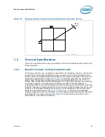
Page 79: ...processor remains within the minimum and maximum case temperature TC specifications when operating at or below the Thermal Design Power TDP value listed per frequency in Table 27 Thermal solutions not designed to provide this level of thermal capability may affect the long term reliability of the processor and system For more details on thermal solution design refer to the appropriate Thermal and ...

Page 80: ...imum TC will vary depending on the TDP of the individual processor Refer to thermal profile figure and associated table for the allowed combinations of power and TC Extended HALT Power W 3 3 Refer to the Component Identification Information section of the Intel Core 2 Extreme Processor X6800 and Intel Core 2 Duo Desktop Processor E6000 and E4000 Sequence Specification Update for processor specific...

Page 81: ...mum Tc C Power Maximum Tc C 0 44 7 24 54 8 48 64 9 2 45 5 26 55 6 50 65 7 4 46 4 28 56 5 52 66 5 6 47 2 30 57 3 54 67 4 8 48 1 32 58 1 56 68 2 10 48 9 34 59 0 58 69 1 12 49 7 36 59 8 60 69 9 14 50 6 38 60 7 62 70 7 16 51 4 40 61 5 64 71 6 18 52 3 42 62 3 65 72 0 20 53 1 44 63 2 22 53 9 46 64 0 Figure 20 Thermal Profile Intel Core 2 Duo Desktop Processor E6x50 Sequence and E6540 with 4 MB L2 Cache ...

Page 82: ... 4 48 55 7 2 43 7 26 50 0 50 56 2 4 44 2 28 50 5 52 56 7 6 44 8 30 51 0 54 57 2 8 45 3 32 51 5 56 57 8 10 45 8 34 52 0 58 58 3 12 46 3 36 52 6 60 58 8 14 46 8 38 53 1 62 59 3 16 47 4 40 53 6 64 59 8 18 47 9 42 54 1 65 60 1 20 48 4 44 54 6 22 48 9 46 55 2 Figure 21 Thermal Profile Intel Core Duo Desktop Processor E6000 Sequence with 4 MB L2 Cache y 0 26x 43 2 40 0 45 0 50 0 55 0 60 0 65 0 0 10 20 3...

Page 83: ...mum Tc C Power Maximum Tc C 0 45 3 24 55 6 48 65 9 2 46 2 26 56 5 50 66 8 4 47 0 28 57 3 52 67 7 6 47 9 30 58 2 54 68 5 8 48 7 32 59 1 56 69 4 10 49 6 34 59 9 58 70 2 12 50 5 36 60 8 60 71 1 14 51 3 38 61 6 62 72 0 16 52 2 40 62 5 64 72 8 18 53 0 42 63 4 65 73 3 20 53 9 44 64 2 22 54 8 46 65 1 Figure 22 Thermal Profile Intel Core 2 Duo Desktop Processor E4500 and E4600 with 2 MB L2 Cache ...

Page 84: ... 9 48 56 6 2 43 8 26 50 5 50 57 2 4 44 3 28 51 0 52 57 8 6 44 9 30 51 6 54 58 3 8 45 4 32 52 2 56 58 9 10 46 0 34 52 7 58 59 4 12 46 6 36 53 3 60 60 0 14 47 1 38 53 8 62 60 6 16 47 7 40 54 4 64 61 1 18 48 2 42 55 0 65 61 4 20 48 8 44 55 5 22 49 4 46 56 1 Figure 23 Thermal Profile Intel Core Duo Desktop Processor E6000 and E4000 Sequence with 2 MB L2 Cache y 0 28x 43 2 40 0 45 0 50 0 55 0 60 0 65 0...

Page 85: ...49 6 54 55 6 4 44 1 30 50 1 56 56 1 6 44 6 32 50 6 58 56 5 8 45 0 34 51 0 60 57 0 10 45 5 36 51 5 62 57 5 12 46 0 38 51 9 64 57 9 14 46 4 40 52 4 66 58 2 16 46 9 42 52 9 68 58 8 18 47 3 44 53 3 70 59 3 20 47 8 46 53 8 72 59 8 22 48 3 48 54 2 74 60 2 24 48 7 50 54 7 75 60 4 Figure 24 Thermal Profile Intel Core 2 Extreme Processor X6800 y 0 23x 43 2 40 0 45 0 50 0 55 0 60 0 65 0 0 10 20 30 40 50 60 ...

Page 86: ...Thermal Monitor feature is enabled and a high temperature situation exists i e TCC is active the clocks will be modulated by alternately turning the clocks off and on at a duty cycle specific to the processor typically 30 50 Clocks often will not be off for more than 3 0 microseconds when the TCC is active Cycle times are processor speed dependent and will decrease as processor core frequencies in...

Page 87: ...o FSB multiple used by the processor is that contained in the appropriate MSR and the VID is that specified in Table 5 These parameters represent normal system operation The second operating point consists of both a lower operating frequency and voltage When the TCC is activated the processor automatically transitions to the new frequency This transition occurs very rapidly on the order of 5 μs Du...

Page 88: ...onsumption This mechanism is referred to as On Demand mode and is distinct from the Thermal Monitor and Thermal Monitor 2 features On Demand mode is intended as a means to reduce system level power consumption Systems must not rely on software usage of this mechanism to limit the processor temperature If bit 4 of the IA32_CLOCK_MODULATION MSR is set to a 1 the processor will immediately reduce its...

Page 89: ... means for thermal protection of system components PROCHOT can allow VR thermal designs to target maximum sustained current instead of maximum current Systems should still provide proper cooling for the VR and rely on PROCHOT only as a backup in case of system cooling failure The system thermal design should allow the power delivery circuitry to operate within its temperature specification even wh...

Page 90: ...ermal profile in Table 29 otherwise the processor temperature can be maintained at TCONTROL or lower as measured by the thermal diode NOTES 1 Intel does not support or recommend operation of the thermal diode under reverse bias 2 Characterized across a temperature range of 50 80 C 3 Not 100 tested Specified by design characterization 4 The ideality factor n represents the deviation from ideal diod...

Page 91: ...the transistor base emitter junction same nodes as VD k Boltzmann Constant and T absolute temperature Kelvin 6 The series resistance RT provided in the Diode Model Table Table 33 can be used for more accurate readings as needed The processor does not support the diode correction offset that exists on other Intel processors Table 34 Thermal Diode Parameters using Transistor Model Symbol Parameter M...

Page 92: ...ermal Management Fan speed control solutions based on PECI uses a TCONTROL value stored in the processor IA32_TEMPERATURE_TARGET MSR The TCONTROL MSR uses the same offset temperature format as PECI though it contains no sign bit Thermal management devices should infer the TCONTROL value as negative Thermal management algorithms should use the relative temperature value delivered over PECI in conju...

Page 93: ...ax Fan Speed RPM TCONTROL Setting TCC Activation Temperature PECI 0 PECI 10 PECI 20 Temperature Note Not intended to depict actual implementation Figure 29 Conceptual Fan Control on Thermal Diode Based Platforms Min Max Fan Speed RPM TCONTROL Setting TCC Activation Temperature TDIODE 90 C TDIODE 80 C TDIODE 70 C Temperature ...

Page 94: ...ere the PECI is know to be unresponsive Prior to a power on RESET and during RESET assertion PECI is not ensured to provide reliable thermal data System designs should implement a default power on condition that ensures proper processor operation during the time frame when reliable data is not available via PECI To protect platforms from potential operational or safety issues due to an abnormal co...

Page 95: ...the use of AutoHALT and Stop Grant states to reduce power consumption by stopping the clock to internal sections of the processor depending on each particular state See Figure 30 for a visual representation of the processor low power states Table 37 Power On Configuration Option Signals Configuration Option Signal1 2 3 NOTES 1 Asserting this signal during RESET will select the corresponding option...

Page 96: ...eration The processor transitions to the Normal state upon the occurrence of SMI INIT or LINT 1 0 NMI INTR RESET causes the processor to immediately initialize itself The return from a System Management Interrupt SMI handler can be to either Normal Mode or the HALT Power Down state See the Intel Architecture Software Developer s Manual Volume III System Programmer s Guide for more information Figu...

Page 97: ... lower frequency transitions the VID to the original value and then changes the bus ratio back to the original value 6 2 3 Stop Grant and Extended Stop Grant States The processor supports the Stop Grant and Extended Stop Grant states The Extended Stop Grant state is a feature that must be configured and enabled via the BIOS Refer to the following sections for details about the Stop Grant and Exten...

Page 98: ...ate until the snoop on the FSB has been serviced whether by the processor or another agent on the FSB After the snoop is serviced the processor returns to the Stop Grant state or HALT Power Down state as appropriate 6 2 4 2 Extended HALT Snoop State Extended Stop Grant Snoop State The processor will remain in the lower bus ratio and VID operating point of the Extended HALT state or Extended Stop G...

Page 99: ...umption the voltage is altered in step with the bus ratio The following are key features of Enhanced Intel SpeedStep Technology Multiple voltage frequency operating points provide optimal performance at reduced power consumption Voltage frequency selection is software controlled by writing to processor MSRs Model Specific Registers thus eliminating chipset dependency If the target frequency is hig...

Page 100: ...Features 100 Datasheet ...

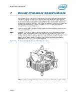
Page 101: ...cal representation of a boxed processor Note Unless otherwise noted all figures in this chapter are dimensioned in millimeters and inches in brackets Note Drawings in this section reflect only the specifications on the Intel boxed processor product These dimensions should not be used as a generic keep out zone for all cooling solutions It is the system designers responsibility to consider their pr...

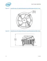
Page 102: ...oxed processor with assembled fan heatsink are shown in Figure 32 Side View and Figure 33 Top View The airspace requirements for the boxed processor fan heatsink must also be incorporated into new baseboard and system designs Airspace requirements are shown in Figure 37 and Figure 38 Note that some figures have centerlines shown marked with alphabetic designations to clarify relative dimensioning ...

Page 103: ... supply A fan power cable will be shipped with the boxed processor to draw power from a power header on the baseboard The power cable connector and pinout are shown in Figure 35 Baseboards must provide a matched power header to support the boxed processor Table 38 contains specifications for the input and output signals at the fan heatsink connector The fan heatsink outputs a SENSE signal that is ...

Page 104: ...Heatsink Power Cable Connector Description Table 38 Fan Heatsink Power and Signal Specifications Description Min Typ Max Unit Notes 12 V 12 volt fan power supply 11 4 12 12 6 V IC Maximum fan steady state current draw Average fan steady state current draw Max fan start up current draw Fan start up current draw maximum duration 1 2 0 5 2 2 1 0 A A A Second SENSE SENSE frequency 2 pulses per fan rev...

Page 105: ...7 in chassis that provide good thermal management For the boxed processor fan heatsink to operate properly it is critical that the airflow provided to the fan heatsink is unimpeded Airflow of the fan heatsink is into the center and out of the sides of the fan heatsink Airspace is required around the fan to ensure that the airflow through the fan heatsink is not blocked Blocking the airflow to the ...

Page 106: ...xed Processor Specifications 106 Datasheet Figure 37 Boxed Processor Fan Heatsink Airspace Keepout Requirements side 1 view Figure 38 Boxed Processor Fan Heatsink Airspace Keepout Requirements Side 2 View ...

Page 107: ...or See Table 39 for specific requirements 7 3 3 Fan Speed Control Operation Intel Core2 Duo Desktop Processor E6000 and E4000 Sequences Only If the boxed processor fan heatsink 4 pin connector is connected to a 3 pin motherboard header it will operate as follows The boxed processor fan will operate at different speeds over a short range of internal chassis temperatures This allows the processor fa...

Page 108: ...e use of an ASIC located on the motherboard that sends out a PWM control signal to the 4th pin of the connector labeled as CONTROL The fan speed is based on actual processor temperature instead of internal ambient chassis temperatures Figure 39 Boxed Processor Fan Heatsink Set Points Table 39 Fan Heatsink Power and Signal Specifications Boxed Processor Fan Heatsink Set Point C Boxed Processor Fan ...

Page 109: ...trolled mode allowing compatibility with existing 3 pin baseboard designs Under thermistor controlled mode the fan RPM is automatically varied based on the Tinlet temperature measured by a thermistor located at the fan inlet For more details on specific motherboard requirements for 4 wire based fan speed control refer to the appropriate Thermal and Mechanical Design Guidelines see Section 1 2 ...

Page 110: ...Boxed Processor Specifications 110 Datasheet ...

Page 111: ...ical representation of a boxed processor in the 775 land LGA package with a Type I TMA Figure 41 illustrates a mechanical representation of a boxed processor in the 775 land LGA package with Type II TMA Note Unless otherwise noted all figures in this chapter are dimensioned in millimeters and inches in brackets Note Drawings in this section reflect only the specifications on the Intel boxed proces...

Page 112: ...section documents the mechanical specifications of the boxed processor TMA The boxed processor will be shipped with an unattached TMA Figure 42 shows a mechanical representation of the boxed processor in the 775 land LGA package for Type I TMA Figure 43 shows a mechanical representation of the boxed processor in the 775 land LGA package for Type II TMA The physical space requirements and dimension...

Page 113: ... BTX Boxed Processor Specifications NOTE Diagram does not show the attached hardware for the clip design and is provided only as a mechanical representation Figure 42 Requirements for the Balanced Technology Extended BTX Type I Keep out Volumes ...

Page 114: ...ght The boxed processor thermal module assembly for Type I BTX will not weigh more than 1200 grams The boxed processor thermal module assembly for Type II BTX will not weigh more than 1200 grams See Chapter 3 and the appropriate Thermal and Mechanical Design Guidelines see Section 1 2 for details on the processor weight and thermal module assembly requirements Figure 43 Requirements for the Balanc...

Page 115: ...ach clip assembly duct and screws for attachment The SRM must be supplied by the chassis hardware vendor See the Support and Retention Module SRM External Design Requirements Document Balanced Technology Extended BTX System Design Guide and the appropriate Thermal and Mechanical Design Guidelines see Section 1 2 for more detailed information regarding the support and retention module and chassis i...

Page 116: ...gnal is not used pin 3 of the connector should be tied to GND The TMA receives a Pulse Width Modulation PWM signal from the motherboard from the 4th pin of the connector labeled as CONTROL Note The boxed processor s TMA requires a constant 12 V supplied to pin 2 and does not support variable voltage control or 3 pin PWM control The power header on the baseboard must be positioned to allow the TMA ...

Page 117: ... start up current draw Fan start up current draw maximum duration 1 0 1 5 2 0 1 0 A A Second SENSE SENSE frequency 2 pulses per fan revolution 1 NOTES 1 Baseboard should pull this pin up to 5V with a resistor CONTROL 21 25 28 kHz 2 3 2 Open Drain Type Pulse Width Modulated 3 Fan will have a pull up resistor for this signal to maximum 5 25 V Figure 46 Balanced Technology Extended BTX Mainboard Powe...

Page 118: ...ature specification is the responsibility of the system integrator In addition Type I TMA must be used with Type I chassis only and Type II TMA with Type II chassis only Type I TMA will not fit in a Type II chassis due to the height difference In the event a Type II TMA is installed in a Type I chassis the gasket on the chassis will not seal against the Type II TMA and poor acoustic performance wi...

Page 119: ... It allows better granularity of fan speed and lowers overall fan speed than a voltage controlled fan Fan RPM is modulated through the use of an ASIC located on Figure 47 Boxed Processor TMA Set Points Table 41 TMA Set Points for 3 wire operation of BTX Type I and Type II Boxed Processors Boxed Processor TMA Set Point ºC Boxed Processor Fan Speed Notes X 23 When the internal chassis temperature is...

Page 120: ...n in the TMA solution is connected to a 3 pin baseboard processor fan header it will default back to a thermistor controlled mode allowing compatibility with existing 3 pin baseboard designs Under thermistor controlled mode the fan RPM is automatically varied based on the Tinlet temperature measured by a thermistor located at the fan inlet For more details on specific motherboard requirements for ...

Page 121: ...sor lands plug into a socket on the LAI Cabling that is part of the LAI egresses the system to allow an electrical connection between the processor and a logic analyzer The maximum volume occupied by the LAI known as the keepout volume as well as the cable egress restrictions should be obtained from the logic analyzer vendor System designers must make sure that the keepout volume remains unobstruc...

Page 122: ...Debug Tools Specifications 122 Datasheet ...
Reviews: