Intel 82555 Datasheet Download Page 54

82555 — Networking Silicon

50


Datasheet

11.4.8

10BASE-T Normal Link Pulse (NLP) Timing Parameters 

11.4.9

Auto-Negotiation Fast Link Pulse (FLP) Timing Parameters 

T26a

T

R_CRSL

End of receive frame to falling 
edge of CRS

10 Mbps

4.5

bits

T27

T

R_RXDVL

End of receive frame to falling 
edge of RXDV

100 Mbps

12

bits

T27a

T

R_RXDVL

End of receive frame to falling 
edge of RXDV

10 Mbps

4

bits

Symbol

Parameter

Conditions

Min

Typ

Max

Units

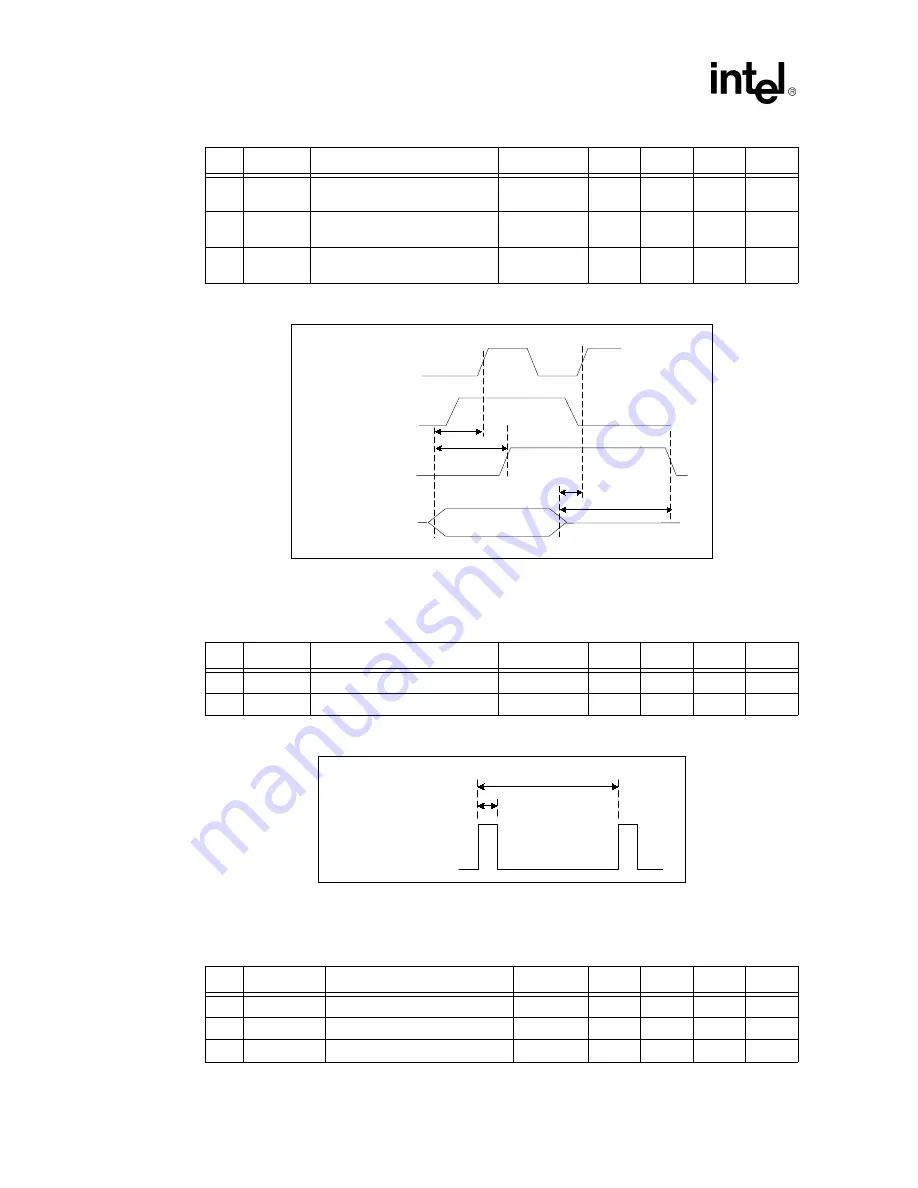
Figure 22. Receive Packet Timing Parameters

R X D V

C R S

Valid Frame Data

R X C L K

Frame On link

T25,T25a

T24,T24a

T26,T26a

T27,T27a

Symbol

Parameter

Conditions

Min

Typ

Max

Units

T28

T

NLP_WID

NLP width

10 Mbps

100

ns

T29

T

NLP_PER

NLP period

10 Mbps

8

24

ms

Figure 23. Normal Link Pulse Timing Parameters

N o r m a l   L i n k   P u l s e

T 2 9

T 2 8

Symbol

Parameter

Conditions

Min

Typ

Max

Units

T30

T

FLP_WID

FLP width (clock/data)

100

ns

T31

T

FLP_CLK_CLK

Clock pulse to clock pulse period

111

125

139

µ

s

T32

T

FLP_CLK_DAT

Clock pulse to data pulse period

55.5

62.5

69.5

µ

s

Summary of Contents for 82555

Page 1: ...a MDI Low external component count Single 25 MHz clock support for 10 Mbps and 100 Mbps crystal or oscillator Single magnetics for 10 Mbps and 100 Mbps operation QFP 100 pin package Performance enhanc...

Page 2: ...ding liability or warranties relating to fitness for a particular purpose merchantability or infringement of any patent copyright or other intellectual property right Intel products are not intended f...

Page 3: ...er 14 4 2 3 100BASE TX Transmit Framing 15 4 2 4 Transmit Driver 16 4 3 100BASE TX Receive Blocks 16 4 3 1 Adaptive Equalizer 17 4 3 2 Receive Clock and Data Recovery 17 4 3 3 MLT 3 Decoder Descramble...

Page 4: ...10 4 Test Port 41 11 0 ELECTRICAL SPECIFICATIONS AND TIMING PARAMETERS 43 11 1 Absolute Maximum Ratings 43 11 2 General Operating Conditions 43 11 3 DC Characteristics 43 11 3 1 MII DC Characteristic...

Page 5: ...cuments the 82555 may be referred to as the DTE Physical Medium Device PMD or Physical Layer Medium PLM It supports a direct glueless interface to Intel components such as the 82557 Fast Ethernet cont...

Page 6: ...tasheet The 82555 also complies with the IEEE 802 3u Auto Negotiation and the IEEE 802 3x Full Duplex Flow Control sections The MAC interface on the 82555 is a superset of the IEEE 802 3u Media Indepe...

Page 7: ...o the analog transmit subsection This includes 4B 5B encoding decoding scrambling descrambling carrier sense collision detection link detection Auto Negotiation data validation and providing MII to th...

Page 8: ...82555 operation in 100BASE TX mode Manchester encoding and decoding is used instead of 4B 5B encoding decoding and scrambling descrambling In addition the Transmit Clock and Receive Clock MII clock si...

Page 9: ...55 Solution 82557 Flash optional EEPROM optional PCI Bus Signals 82555 RXD 3 0 RXC RXERR RXDV CRS COL TXD 3 0 TXC TXEN MDC MDIO RESET Table 1 82555 MII Signal Name Description Direction Clock Referenc...

Page 10: ...82555 Networking Silicon 6 Datasheet TXERR Transmit Error repeater mode only From RIC TXC Yes Table 1 82555 MII Signal Name Description Direction Clock Reference MII Signal Supported by the 82555...

Page 11: ...logic voltage levels except the X1 and X2 crystal signals The transmit differential and receive differential pins are specified as analog outputs and inputs respectively The figure below show the pin...

Page 12: ...crystal should have a tolerance of 50 PPM or better X2 55 O Crystal Output Two X1 and X2 can be driven by an external 25 MHz crystal Otherwise X1 may be driven by an external MOS level 25 MHz oscilla...

Page 13: ...pically clocked by a receiver interface device TXEN 79 I Transmit Enable The Transmit Enable signal indicates to the 82555 that valid data is present on the TXD 3 0 pins TXERR 59 I Transmit Error The...

Page 14: ...is the highest common technology between the 82555 and its link partner Symbol Pin Type Name and Function ACTLED 12 O Activity LED This signal indicates either transmit or receive activity When activi...

Page 15: ...for address port configuration Link Status In DTE adapter mode if T4 Advance is active the LISTAT_N signal is active low and the slave PHY link is valid PHYA1 TEXEC 25 I This pin is multiplexed and c...

Page 16: ...wer and Ground Pins Symbol Pin Type Name and Function VCC 7 9 15 17 19 27 29 31 36 38 40 45 58 62 64 66 73 75 83 88 93 98 I Power 5 V 5 VSS 3 8 10 14 16 18 20 26 28 30 32 35 37 39 41 46 49 53 57 61 63...

Page 17: ...B 5B encoder accepts nibble wide data 4 bits from the MAC and compiles it into 5 bit wide parallel symbols These symbols are scrambled and serialized into a 125 Mbps bit stream converted by the analog...

Page 18: ...stream from the scrambler and encodes the stream into MLT 3 for presentation to the driver MLT 3 is similar to NRZI coding but three levels are output instead of two There are three output levels posi...

Page 19: ...dundancy Check CRC When TXEN is asserted the 82555 accepts data on the MII TXD 3 0 lines encodes it and sends it out onto the wire The 82555 encodes the first byte of the preamble as the JK symbol enc...

Page 20: ...0BASE TX mode should also work in 10BASE T mode The following is a list of current magnetics modules available from several vendors 4 3 100BASE TX Receive Blocks The receive subsection of the 82555 ac...

Page 21: ...the wire and the preamble or start of frame delimiter When two non consecutive bits are 0b within 10 bits 125 Mbps 5B data coding the 82555 immediately asserts the CRS signal When the JK symbols 11000...

Page 22: ...uration If the T4ADV pin is active the Auto Negotiation function will advertise and negotiate T4 technology Speed and duplex auto select are functions of Auto Negotiation However these parameters may...

Page 23: ...and Normal Link Pulses NLPs are detected the 82555 defaults to 10 Mbps operation If the 82555 detects a speed change it dynamically changes its transmit clock and receive clock frequencies to the app...

Page 24: ...82555 Networking Silicon 20 Datasheet...

Page 25: ...sharing the same magnetics In 10 Mbps mode the 82555 begins transmitting the serial Manchester bit stream within 3 bit times 300 nanoseconds after the MAC asserts TXEN In 10 Mbps mode the line drivers...

Page 26: ...he idle state during reception before the end of frame bit is detected 250 nanoseconds without mid bit transitions 5 4 10BASE T Collision Detection Collision detection in 10 Mbps mode is indicated by...

Page 27: ...on the squelch test and the carrier sense transmit function This allows the 82555 to transmit and receive simultaneously achieving up to 20 Mbps of network bandwidth The configuration can be achieved...

Page 28: ...82555 Networking Silicon 24 Datasheet...

Page 29: ...s a feature for hub management allowing a 10 100 Mbps repeater design to automatically detect whether or not it can operate at 100 Mbps If the ANDIS signal is de asserted the Auto Negotiation feature...

Page 30: ...e connected from each of the 82555 devices to the specified RIC pin The figure below illustrates an example of multiple 82555s connected to a 25 MHz or 2 5 MHz oscillator Figure 9 Clock Signal Example...

Page 31: ...ation by the 82555 ST This field contains the value of 01b indicating the start of a frame OP This is a 2 bit field containing one of the following two operation codes 10b read or 01b write PHYAD This...

Page 32: ...their default states and is self clearing The PHY returns a value of 1b until the reset process has completed and accepts a read or write transaction 1 PHY Reset 0 Normal operation 0 RW SC 14 Loopbac...

Page 33: ...d to the mode which the 82555 can operate When the 82555 is placed in Loopback mode the behavior of the PHY shall not be affected by the status of this bit bit 8 1 Full Duplex 0 Half Duplex 0 RW 7 Col...

Page 34: ...k detected 0 RO LL SC 1 Jabber Detect 1 Jabber condition detected 0 No jabber condition detected 0 RO LH SC 0 Extended Capability 1 Extended register capabilities enabled 0 No extended register capabi...

Page 35: ...n ability RO 12 5 Technology Ability Field This bit reflects the 82555 s link partner s Auto Negotiation ability RO 4 0 Selector Field This bit reflects the 82555 s link partner s Auto Negotiation abi...

Page 36: ...11 Receive De Serializer In Sync Indication This bit indicates status of the 100BASE TX Receive De Serializer In Sync RO 10 100BASE TX Power Down This bit indicates the power state of 100BASE TX 82555...

Page 37: ...Normal filter operation 0 RW 4 Auto Polarity Disable 1 Auto Polarity disabled 0 Normal polarity operation 0 RW 3 Squelch Disable 1 10BASE T squelch test disable 0 Normal squelch operation 0 RW 2 Exten...

Page 38: ...rame This field contains a 16 bit counter that increments for each premature end of frame event The counter stops when full and does not roll over and self clears on read A frame without a TR at the e...

Page 39: ...itialization time Once the link is established by this handshake the native link pulse scheme resumes that is 10BASE T or 100BASE TX link pulses A reset or management renegotiate command through the M...

Page 40: ...wledge bit set 5 Determine operating mode via the priority table 6 Receive FLP from the link partner and record FLP in the MII register 8 2 Parallel Detect and Auto Negotiation The 82555 automatically...

Page 41: ...th FLPs and link integrity pulses The following diagram illustrates this process Figure 10 Auto Negotiation and Parallel Detect Force_Fail Ability detect either by parallel detect or auto negotiation...

Page 42: ...82555 Networking Silicon 38 Datasheet...

Page 43: ...g receive when the 82555 is not in loopback mode Speed This LED will be on if a 100BASE TX link is detected and off if a 10BASE T link is detected If the link fails while in Auto Negotiation this LED...

Page 44: ...82555 Networking Silicon 40 Datasheet...

Page 45: ...ed by a simple mechanism and handshake Activation of all test modes requires simple hardware The TAP signals connected to the 82555 blocks and periphery control the 82555 s mode of operation to allow...

Page 46: ...5 can wake up during high Z mode or NAND Test which can be harmful to the board The TAP should be reset only with a hardware reset input pin and not with software reset The TOUT control logic selects...

Page 47: ...ional sections of this specification is not implied Ex posure to absolute maximum rating conditions for extended periods may affect device reliability All output voltages 0 5 7 0 V VOTD Transmit Data...

Page 48: ...tive load across the receive differential pins RDP and RDN c Transmitter current is measured with a 1 1 transformer on the center tap d Current is measured on all VCC pins at VCC 5 25 V e The analog p...

Page 49: ...measured on all VCC pins at VCC 5 25 V Symbol Parameter Description Condition Min Typ Max Units Figure 12 RBIAS100 Resistance versus ICCT100 667 634 604 38mA 40mA 42mA Icct100 Rbias100 Figure 13 AC Te...

Page 50: ...fter the rising edge of TXC 0 ns T9 TRXSU RXD 3 0 RXDV RXERR valid before the rising edge of RXC 10 ns T10 TRXH RXD 3 0 RXDV RXERR hold time after the rising edge of RXC 10 ns T11 TMSU MDIO setup time...

Page 51: ...lid Data Invalid Data Valid T13 MDIO Output Data Invalid Data Invalid Data Valid Symbol Parameter Conditions Min Typ Max Units T14 TRDRV PORTEN assertion to RXD 3 0 RXDV and RXERR RXC driven 1 5 2 5 R...

Page 52: ...bits T17 TXEN_END TXC on first TXEN inactive to end of frame 100 Mbps 17 bits T17a TXEN_END TXC on first TXEN inactive to end of frame 10 Mbps 5 bits T18 TXEN_CRSL TXC on first TXEN inactive to falli...

Page 53: ...TXEN de asserted to falling edge of COL 10 Mbps 410 ms Figure 21 Jabber Timing Parameters TXEN COL TDP TDN T22 T23 Symbol Parameter Conditions Min Typ Max Units T24 TR_CRSH Start of receive frame to r...

Page 54: ...bol Parameter Conditions Min Typ Max Units Figure 22 Receive Packet Timing Parameters RXDV CRS Valid Frame Data RXCLK Frame On link T25 T25a T24 T24a T26 T26a T27 T27a Symbol Parameter Conditions Min...

Page 55: ...ions Min Typ Max Units Figure 24 Fast Link Pulse Timing Parameters Fast Link Pulse T31 T30 T30 Clock Pulse Data Pulse Clock Pulse FLP Bursts T34 T35 Symbol Parameter Conditions Min Typ Max Units T36 T...

Page 56: ...asheet 11 4 12 100BASE TX Transmitter AC Specification Figure 26 X1 Clock Specifications T38 2 5V T39 T39 0 4V 4 0V Symbol Parameter Conditions Min Typ Max Units T40 TJIT TDP TDN differential output p...

Page 57: ...27 Dimension Diagram for the 82555 QFP Table 7 Dimensions for the 82555 QFP Symbol Description Min Norm Max N Lead Count 100 A Overall Height 3 15 A1 Stand Off 0 05 0 40 b Lead Width 0 20 0 30 0 40 c...

Page 58: ...82555 Networking Silicon 54 Datasheet T Lead Angle 0 0 10 0 Y Coplanarity 0 10 Table 7 Dimensions for the 82555 QFP Symbol Description Min Norm Max...

Reviews: