Figure 22
Schematics Sheet 9
TLE987x EvalBoard
9 Schematics and layout baseboard
User Manual
26
v1.0
2020-07-30
Page 1: ...ormation about the layout jumper settings interface and debug options It introduces the evaluation platform as well as how to write software and download it to the TLE987x The TLE987x is available in VQFN and a brand new TQFP package this document is valid for both Intended audience This document is for everyone who works with the TLE987x EvalBoard User Manual Please read the Important Notice and ...
Page 2: ... Input Slave Output MON Monitor MOSI Master Output Slave Input N C Not connected n u Not used OP1 Negative operational amplifier input OP2 Positive operational amplifier input PORST Power on Reset SCLK Serial Clock SH1 3 Source high side MOSFET 1 3 SINN Sinusoidal TMR output negative SINP Sinusoidal TMR output positive SL Source low side MOSFET SWD Arm serial wire debug TMS Test mode select TMR Tu...
Page 3: ...C Core supply VDDEXT External voltage supply output VDDP I O port supply VDH Voltage drain high side MOSFET VS Battery supply input VSD Battery supply input for MOSFET driver TLE987x EvalBoard Abbreviations and definitions User Manual 3 v1 0 2020 07 30 ...
Page 4: ...on ConfigWizard 13 6 3 TLE987x SDK 13 6 4 Debug connection setup 13 7 Technical data 15 8 Optional additional placements 16 9 Schematics and layout baseboard 18 9 1 Schematics baseboard 18 9 2 Layout baseboard 28 10 Schematics and layout VQFN socket 30 10 1 Schematics VQFN socket 30 10 2 Layout VQFN socket 31 11 Schematics and layout TQFP socket 32 11 1 Schematics TQFP socket 32 11 2 Layout TQFP s...
Page 5: ...ge supply Three MOSFET half bridges are placed on the board to drive a BLDC motor The board is ready to be connected to a car supply or similar and offers an USB port to use the on board SWD debugger The evaluation board can be operated by standard laboratory equipment since the power supply and LIN communication are connected using via banana jacks A LED indicates that the board is connected corr...
Page 6: ...nication via banana jack Banana jacks for motor connection The three jacks for Phase 1 Phase 2 and Phase 3 provide access to the three half bridges and for driving a brushless motor uIO Stick connector The uIO bootstrap loader is a 16 pin header 2 8 with 2 54 mm pitch This interface can be used to programming the TLE987x via LIN see www infineon com uio or www hitex com uio TLE987x EvalBoard 2 Int...
Page 7: ... PORST Figure 4 Pin configuration SWD interface Pin header for SPI The 12 pin header 2 6 with 2 54 mm pitch can be used for controlling an external IC with the SPI In order to access the SPI the jumpers P0 4 and P1 2 have to be set in position 2 2 4 6 1 3 5 8 10 7 9 12 11 VDDP GND SCLK MISO MOSI CS VDDP GND SCLK MISO MOSI CS Figure 5 Pin configuration SPI Pin header for Hall sensor interface The 1...
Page 8: ...erface Pin header for TMR sensor interface The 10 pin header 2 5 with 2 54 mm pitch can be used for controlling external TMR sensors In order to access the TMR sensor interface the jumpers SINN and SINP have to be set Figure 7 Pin configuration TMR sensor interface TLE987x EvalBoard 2 Interconnects User Manual 8 v1 0 2020 07 30 ...
Page 9: ...nts Test points 2 VBAT 1 VS 1 VCP 8 GND 2 SH1 2 SH2 2 SH3 2 GH1 2 GH2 2 GH3 for gate current supervision 3 GH1 3 GH2 3 GH3 for gate current supervision OP1 OP2 3 VDH LEDs LEDBAT supply voltage active LEDCOM on board debugger communication active LEDVDDEXT VDDEXT active LED1 8 can be connected to GPIOs see Table 1 TLE987x EvalBoard 3 Test points and LEDs User Manual 9 v1 0 2020 07 30 ...
Page 10: ...N button to MON pin Open it to disconnect MON button from MON pin VDDEXT_LED Set this jumper to enable LED operation at VDDEXT ILoadVS This jumper is closed by default If this jumper is left open the device is not supplied Target is to measure the current flowing into the TLE987x device ILoadVSD This jumper is closed by default If this jumper is left open the charge pump is not supplied Target is ...
Page 11: ... 4 P0 4 HALL B CS P1 2 HALL C MISO Figure 11 Jumper position for LEDs and PINs Set jumper as shown in Figure 11 to connect the according PINs and LEDs Table 1 LEDs and PORTs jumper PIN LED P0 1 LED1 P0 2 LED2 P0 3 LED3 P1 2 LED4 P1 0 LED5 P1 3 LED6 P1 4 LED7 P0 4 LED8 TLE987x EvalBoard 4 Jumper settings User Manual 11 v1 0 2020 07 30 ...
Page 12: ...e single wire banana interface The BSL interface programs the device via LIN For further information about the uIO interface is available at www infineon com uio or www hitex com uio 5 2 Debugging Debugging is possible via the on board debugger that can be connected via an USB cable and the SWD interface the signals are routed through the 10 pin header SWD interface TLE987x EvalBoard 5 Communicati...
Page 13: ...ineon Toolbox The Infineon Toolbox allows to download and update all your Infineon tools It can be downloaded from www infineon com toolbox 6 3 TLE987x SDK All Embedded Power products can be installed to Keil µVision5 via Pack Installer Browsing to the Infineon chapter in All Devices will lead to the TLE98xx Series The pack file comes with several code examples to provide an easy start up and spee...
Page 14: ...f the board is connected successfully the Arm IDCODE will be visible in the SW Device Window If the connection fails Connect Reset Options and Port window has to be checked TLE987x EvalBoard 6 Software toolchain User Manual 14 v1 0 2020 07 30 ...
Page 15: ...7 Technical data Table 2 Technical data Voltage supply max 28 V Motor current max 30 A Pin ports 5 V TLE987x EvalBoard 7 Technical data User Manual 15 v1 0 2020 07 30 ...
Page 16: ...oscillator CXTAL1 Oscillator capacitor 1 CXTAL2 Oscillator capacitor 2 RSBHS1 Resistance snubber high side MOSFET phase 1 CSBHS1 Capacitor snubber high side MOSFET phase 1 CGDHS1 Gate drain capacitor high side MOSFET phase 1 CGSHS1 Gate source capacitor high side MOSFET phase 1 RSBLS1 Resistance snubber low side MOSFET phase 1 CSBLS1 Capacitor snubber low side MOSFET phase 1 CGDLS1 Gate drain capa...
Page 17: ...SFET phase2 CGSLS2 Gate source capacitor low side MOSFET phase 2 RSBHS3 Resistance snubber high side MOSFET phase 3 CSBHS3 Capacitor snubber high side MOSFET phase 3 CGDHS3 Gate drain capacitor high side MOSFET phase 3 CGSHS3 Gate source capacitor high side MOSFET phase 3 RSBLS3 Resistance snubber low side MOSFET phase 3 CSBLS3 Capacitor snubber low side MOSFET phase 3 CGDLS3 Gate drain capacitor ...
Page 18: ...9 Schematics and layout baseboard 9 1 Schematics baseboard Figure 14 Schematics Sheet 1 TLE987x EvalBoard 9 Schematics and layout baseboard User Manual 18 v1 0 2020 07 30 ...
Page 19: ...Figure 15 Schematics Sheet 2 TLE987x EvalBoard 9 Schematics and layout baseboard User Manual 19 v1 0 2020 07 30 ...
Page 20: ...Figure 16 Schematics Sheet 3 TLE987x EvalBoard 9 Schematics and layout baseboard User Manual 20 v1 0 2020 07 30 ...
Page 21: ...Figure 17 Schematics Sheet 4 TLE987x EvalBoard 9 Schematics and layout baseboard User Manual 21 v1 0 2020 07 30 ...
Page 22: ...Figure 18 Schematics Sheet 5 TLE987x EvalBoard 9 Schematics and layout baseboard User Manual 22 v1 0 2020 07 30 ...
Page 23: ...Figure 19 Schematics Sheet 6 TLE987x EvalBoard 9 Schematics and layout baseboard User Manual 23 v1 0 2020 07 30 ...
Page 24: ...Figure 20 Schematics Sheet 7 TLE987x EvalBoard 9 Schematics and layout baseboard User Manual 24 v1 0 2020 07 30 ...
Page 25: ...Figure 21 Schematics Sheet 8 TLE987x EvalBoard 9 Schematics and layout baseboard User Manual 25 v1 0 2020 07 30 ...
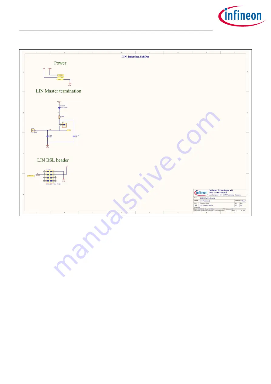
Page 26: ...Figure 22 Schematics Sheet 9 TLE987x EvalBoard 9 Schematics and layout baseboard User Manual 26 v1 0 2020 07 30 ...
Page 27: ...Figure 23 Schematics Sheet 10 TLE987x EvalBoard 9 Schematics and layout baseboard User Manual 27 v1 0 2020 07 30 ...
Page 28: ...9 2 Layout baseboard Figure 24 Top layer Figure 25 Power layer TLE987x EvalBoard 9 Schematics and layout baseboard User Manual 28 v1 0 2020 07 30 ...
Page 29: ...Figure 26 Ground layer Figure 27 Bottom layer TLE987x EvalBoard 9 Schematics and layout baseboard User Manual 29 v1 0 2020 07 30 ...
Page 30: ...10 Schematics and layout VQFN socket 10 1 Schematics VQFN socket Figure 28 Schematics VQFN socket TLE987x EvalBoard 10 Schematics and layout VQFN socket User Manual 30 v1 0 2020 07 30 ...
Page 31: ...10 2 Layout VQFN socket Figure 29 Top layer VQFN socket Figure 30 Bottom layer VQFN socket mirrored TLE987x EvalBoard 10 Schematics and layout VQFN socket User Manual 31 v1 0 2020 07 30 ...
Page 32: ...11 Schematics and layout TQFP socket 11 1 Schematics TQFP socket Figure 31 Schematics TQFP socket TLE987x EvalBoard 11 Schematics and layout TQFP socket User Manual 32 v1 0 2020 07 30 ...
Page 33: ...11 2 Layout TQFP socket Figure 32 Top layer TQFP socket Figure 33 Bottom layer TQFP socket mirrored TLE987x EvalBoard 11 Schematics and layout TQFP socket User Manual 33 v1 0 2020 07 30 ...
Page 34: ...12 Revision history Revision Date Changes v1 0 2020 07 30 Initial creation TLE987x EvalBoard 12 Revision history User Manual 34 v1 0 2020 07 30 ...
Page 35: ...ument is subject to customer s compliance with its obligations stated in this document and any applicable legal requirements norms and standards concerning customer s products and any use of the product of Infineon Technologies in customer s applications The data contained in this document is exclusively intended for technically trained staff It is the responsibility of customer s technical depart...