5
PCB layout
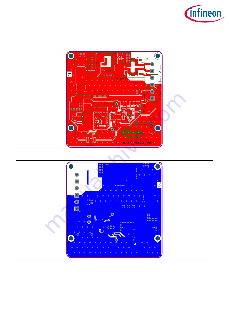
Figure 7
PCB layout top view
Figure 8
PCB layout bottom view
Voltage mode SEPIC evaluation kit
TLD5099EP
5 PCB layout
User guide
8
Rev.2.00
2022-02-04
Page 1: ...9EP voltage mode SEPIC evaluation board Intended audience This document is intended for engineers who need to perform measurements and check performance with TLD5099EP voltage mode SEPIC evaluation bo...
Page 2: ...SEPIC topology without any additional features enabled In this configuration it can deliver up to 12 W to the load with an efficiency above 85 Auxiliary circuits which protect the DC DC and the load d...
Page 3: ...2 s Maximum output current Resistive load 1 A Switching frequency VIN 13 2 V spread spectrum on 400 kHz Efficiency Measured with a 12 power resistor as load 85 Output voltage range Output voltage rel...
Page 4: ...R25 VREF 1 where VOUT is the desired output voltage and VREF 300 mV is the feedback reference voltage Correct device functioning is achieved if voltages VFBH and VFBL on both terminals of R25 are grea...
Page 5: ...ce starts without any external enable signal because pin EN ENABLE is connected directly to the positive rail see Schematics for details Figure 4 Auto enable configuration Voltage mode SEPIC evaluatio...
Page 6: ...3 0 0 0 0 O8 O8 NP W Y U NP W Y U NP W Y U 3 Q R X X P a a b R b R a 1 cS O d 4 N 9 9 0 Y O8 O8 O8 dQ 1 0 1 0 0 8 0 1 0 0 81 4 U1 U1 0 0 1 e0 e0 f X 1 Q f X 1 Q O8 N P V W VO V W VO V W VO O8 0 1 e0 3...
Page 7: ...k W VO f 0 T 1 g Vk V P k V P f 1 T 2 g V P V P O8 0 N 91 0 a 0 1 0 O8 4 N 90 0 a O8 O8 7 7 7 0 O8 0 1 81 81 Q XV 5 2 VQ l 0 0 4 5 2 VQ l 0 0 4 O8 0 1 N 0 j7 j7 4 0 N99 NP W a U O8 O8 0 N 91 1 3 6 a 0...
Page 8: ...5 PCB layout Figure 7 PCB layout top view Figure 8 PCB layout bottom view Voltage mode SEPIC evaluation kit TLD5099EP 5 PCB layout User guide 8 Rev 2 00 2022 02 04...
Page 9: ...MHz TDK MPZ2012S101ATD25 L3 L5 1 k 100 MHz TDK MPZ2012S102ATD25 L4 TDK ACM70V 701 2PL TL00 L7 22 uH TDK B82477D4223M000 Q1 IPD90P04P4L 04 Infineon Technologies IPD90P04P4L 04 Q2 IPD25N06S4L 30 Infine...
Page 10: ...rials Designator Value Manufacturer Manufacturer order number X5 TSM 103 01 S SV Samtec TSM 103 01 S SV X20 D3082 05 Harwin D3082 05 Voltage mode SEPIC evaluation kit TLD5099EP 6 Bill of material User...
Page 11: ...Table 3 Parameters influencing efficiency Output load 12 power resistor EMI filter Totally bypassed by closing the jumpers X1 X14 and X16 Efficiency performances can be increased refer to Maximizing e...
Page 12: ...ting of R5 and C25 or choose a lower value for the capacitor C25 for example 1 nF 2 Bypass the whole EMI filter by bridging the jumpers X1 X14 and X16 3 Bypass the output ferrite beads L3 and L5 4 Rep...
Page 13: ...required the following actions should be considered 1 Choose a higher value for the capacitor C25 for example 2 7 nF or 3 3 nF 2 Include the whole EMI filter by removing bridges from the jumpers X1 X...
Page 14: ...release related to evalboard S01_P01 Editorial changes and rephrasing for clarity Updated all figures Rearranged connectors on evalboard Added ground bar on evalboard Rev 1 00 2020 01 29 First release...
Page 15: ...liabilities of any kind including without limitation warranties of non infringement of intellectual property rights of any third party with respect to any and all information given in this application...