


TLE5012B
Functional Description
User’s Manual
12
Rev. 1.2, 2018-02
configured via SSC interface to use an external clock signal supplied on the IFC pin as the PLL source, instead of
the internal clock. External clock mode is only available in the PWM or SPC interface configurations.
2.2.3
SD-ADC
The
S
igma-
D
elta
A
nalog-
D
igital-
C
onverters (
SD-ADC
) transform the analog GMR voltages and temperature
voltage into the digital domain.
2.2.4
Digital Signal Processing Unit
The Digital Signal Processing Unit (DSPU) contains the:
•
I
ntelligent
S
tate
M
achine (
ISM
), which does error compensation of offset, offset temperature drift, amplitude
synchronicity and orthogonality of the raw signals from the GMR bridges, and performs additional features
such as auto-calibration, prediction and angle speed calculation
•
CO
ordinate
R
otation
DI
gital
C
omputer (
CORDIC
), which contains the trigonometric function for angle
calculation
•
C
apture
C
ompare
U
nit (
CCU
), which is used to generate the PWM and SPC signals
•
R
andom
A
ccess
M
emory (
RAM
), which contains the configuration registers
•
Laser Fuses, which contain the calibration parameters for the error-compensation and the IC default
configuration, which is loaded into the RAM at startup
Laser fuses configuration
The laser fuse settings are derivate specific. During production, each and every TLE5012B chip is specifically
configured according to a derivate interface (PWM, SPC, HSM or IIF) and to its specific calibration values (e.g.
offset, amplitude synchronicity, orthogonality). These default values are set by laser fuses, where they remain
stored permanently. At power-on the values stored in the fuses are loaded into flip-flops (placed in the RAM).
Via the SSC interface, these derivate specific configuration values can be overwritten in the RAM. This allows
some programmability such as change of interface (using a IIF derivate as a PWM derivate for example) or to
correct the calibration values (if running the autocalibration mode for example). It is highly recommended to
configure the sensor with customized settings right after a Hardware reset (within the first 120µs, prior to start of
the Built-In Self-Test). If this interval is not sufficient, it is also possible to configure the sensor after the power-on
time. To ensure a correct configuration after power-on time, see recommendations on
. When powered
off or reset, the overwritten values will be lost and the default values stored in the fuses will be reloaded into the
RAM at the next power up.
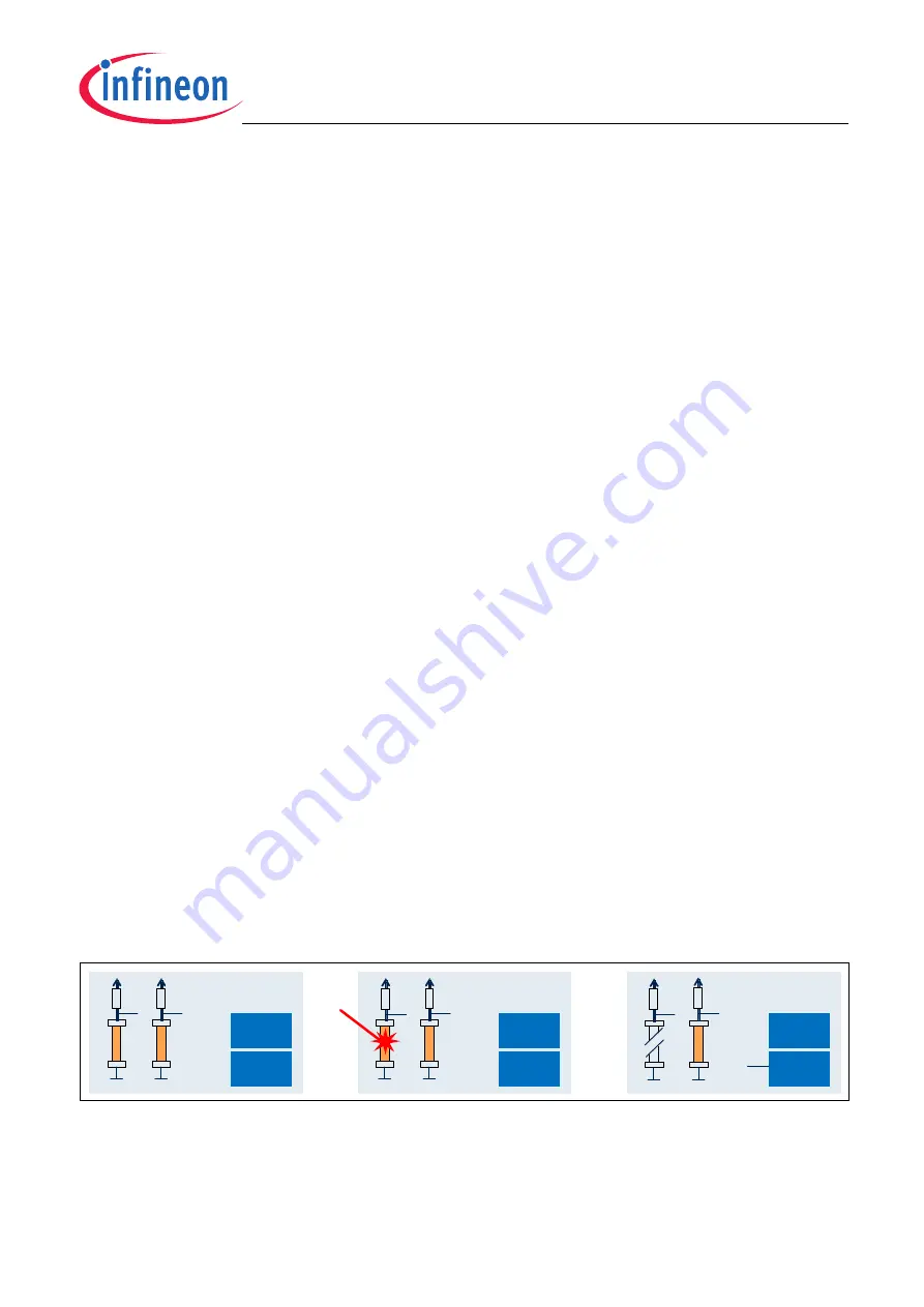
The
shows how the fuse burning process works. In the original state all fuses are connected to ground
(GND). Once the calibration and derivate specific values are calculated, the information is burned into the fuses,
so that some remain connected to GND (“low” or logical “0”) and some are now pulled up by a resistor (“high” or
logical “1”). When powering the sensor, the RAM is initialized with the values from the fuses.
Figure 2-2 Laser Fuses burning process
DSPU
RAM
F
U
S
E
GND
0
F
U
S
E
GND
…
V
DD
0
V
DD
DSPU
RAM
F
U
S
E
GND
F
U
S
E
GND
…
0
V
DD
0
V
DD
DSPU
RAM
GND
F
U
S
E
GND
…
10
0
V
DD
1
V
DD