background image


Page 72 

IOWA-MARK Half-size CPU Card

If the IOWA-MARK fails to boot due to improper BIOS settings, the clear CMOS jumper 

clears the CMOS data and resets the system BIOS information. To do this, use the jumper 

cap to close pins 2 and 3 for a few seconds then reinstall the jumper clip back to pins 1 

and 2. 

If the “CMOS Settings Wrong” message is displayed during the boot up process, the fault 

may be corrected by pressing the F1 to enter the CMOS Setup menu.    Do one of the 

following: 


Enter the correct CMOS setting 


Load Optimal Defaults 


Load Failsafe Defaults.     

After having done one of the above, save the changes and exit the CMOS Setup menu.   

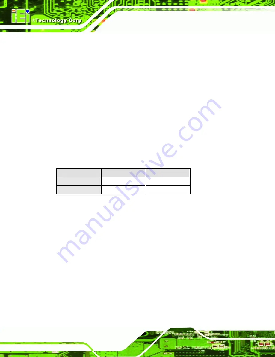
The clear CMOS jumper settings are shown in 

Table 5-2

AT Power Select 

Description 


Short 1 - 2   

Keep CMOS Setup 

Default 

Short 2 - 3 

Clear CMOS Setup 


Table 5-2: Clear CMOS Jumper Settings 

The location of the clear CMOS jumper is shown in 

Figure 5-3 

below. 

Summary of Contents for IOWA-MARK-533-128MB-R10

Page 1: ...IOWA MARK Half size CPU Card Page i...

Page 2: ...IOWA MARK Half size CPU Card Page ii Revision MODEL IOWA MARK VIA MARK Motherboard Revision Number Description Date of Issue 1 0 Initial release December 2006...

Page 3: ...roduct or documentation even if advised of the possibility of such damages This document contains proprietary information protected by copyright All rights are reserved No part of this manual may be r...

Page 4: ...resentative directly To contact an IEI sales representative please send an email to sales iei com tw The items listed below should all be included in the IOWA MARK package 1 x IOWA MARK single board c...

Page 5: ...SUPPORT 12 2 4 1 VIA MARK Overview 12 2 4 2 VIA MARK Memory Support 13 2 4 3 VIA MARK Integration 13 2 4 4 VIA MARK S3 Graphics Unichrome Pro Graphics Core 13 2 4 5 VIA MARK VIA PadLock Security Engi...

Page 6: ...ntents 23 4 CONNECTOR PINOUTS 27 4 1 PERIPHERAL INTERFACE CONNECTORS 28 4 1 1 IOWA MARK Layout 28 4 1 2 Peripheral Interface Connectors 29 4 1 3 External Interface Panel Connectors 30 4 2 INTERNAL PER...

Page 7: ...57 4 3 2 PS 2 Keyboard Mouse Connector 57 4 3 3 RJ 45 Ethernet Connector 58 4 3 4 Serial Port Connector COM 1 59 4 3 5 VGA Connector 60 5 INSTALLATION 63 5 1 ANTI STATIC PRECAUTIONS 64 5 2 INSTALLATIO...

Page 8: ...4 Unable to Reboot After Configuration Changes 87 6 1 5 Main BIOS Menu 87 6 2 STANDARD CMOS FEATURES 90 6 2 1 IDE Primary Master Slave 92 6 3 ADVANCED BIOS FEATURES 95 6 4 ADVANCED CHIPSET FEATURES 1...

Page 9: ...ssing the AC 97 CODEC 178 E 1 2 Driver Installation 178 E 2 SOUND EFFECT CONFIGURATION 178 E 2 1 Accessing the Sound Effects Manager 178 E 2 2 Sound Effect Manager Configuration Options 180 F RAID SET...

Page 10: ...ne to Mainboard Connector Location 35 Figure 4 8 Battery Connector Location 36 Figure 4 9 CF Card Socket Location 37 Figure 4 10 DIO Connector Locations 39 Figure 4 11 5V Fan Connector Location 40 Fig...

Page 11: ...Connection 80 Figure 5 9 SATA Power Drive Connection 81 Figure 5 10 VGA Connector 82 Figure 5 11 PS 2 Connector 84 Figure 7 1 Access the 4in1_Extreme Folder 143 Figure 7 2 Setup Utility Icon 143 Figur...

Page 12: ...l 153 Figure 7 17 Audio Driver Installation Begins 154 Figure 7 18 Audio Driver Installation Complete 155 Figure 7 19 Access the LAN Driver Folder 156 Figure 7 20 Setup Utility Icon 156 Figure 7 21 LA...

Page 13: ...ckplane to Mainboard Connector Pinouts 36 Table 4 8 Battery Connector Pinouts 37 Table 4 9 CF Card Socket Pinouts 38 Table 4 10 DIO Connector Pinouts 39 Table 4 11 5V Fan Connector Pinouts 40 Table 4...

Page 14: ...J 45 Ethernet Connector Pinouts 59 Table 4 27 J7 Connector LEDs 59 Table 4 28 RS 232 Serial Port COM 1 Pinouts 60 Table 4 29 VGA Connector Pinouts 61 Table 5 1 Jumpers 71 Table 5 2 Clear CMOS Jumper S...

Page 15: ...Menu 5 Advanced Chipset Features 104 BIOS Menu 6 Integrated Peripherals 113 BIOS Menu 7 Power Management Setup 121 BIOS Menu 8 Power Management 124 BIOS Menu 9 Wake Up Events 127 BIOS Menu 10 IRQ Act...

Page 16: ...ive FDC Floppy Disk Connector FFIO Flexible File Input Output FIFO First In First Out FSB Front Side Bus IrDA Infrared Data Association HDD Hard Disk Drive IDE Integrated Data Electronics I O Input Ou...

Page 17: ...IOWA MARK Half size CPU Card Page 1 1 Introduction Chapter 1...

Page 18: ...The IOWA MARK series has four models IOWA MARK 533 128MB R10 IOWA MARK 533S 128MB R10 IOWA MARK 800 128MB R10 IOWA MARK 800S 128MB R10 The specifications for the four models are show in Table 1 1 IOWA...

Page 19: ...g term support until December 2010 1 1 3 IOWA MARK Features Some of the IOWA MARK features are listed below Half size form factor RoHS compliant VIA MARK processor installed Dual independent display f...

Page 20: ...Page 4 IOWA MARK Half size CPU Card 1 2 IOWA MARK Overview Figure 1 1 IOWA MARK Overview...

Page 21: ...wer connector 1 x Audio connector 1 x Backlight inverter connector 1 x Backplane to mainboarrd connector 1 x Battery connector 1 x CompactFlash socket 1 x Digital input output DIO connector 1 x Fan co...

Page 22: ...al interface connectors on the board rear panel 1 x Ethernet connector 1 x PS 2 keyboard connector 1 x Serial port connector 1 x VGA connector The IOWA MARK has the following on board jumpers Clear CM...

Page 23: ...00C COM Two RS 232 serial ports one internal one external USB2 0 Four USB 1 1 devices supported IDE One 40 pin IDE connects to two Ultra ATA33 66 100 devices Watchdog Timer Software programmable 1 255...

Page 24: ...Page 8 IOWA MARK Half size CPU Card THIS PAGE IS INTENTIONALLY LEFT BLANK...

Page 25: ...IOWA MARK Half size CPU Card Page 9 2 Detailed Specifications Chapter 2...

Page 26: ...d features of the IOWA MARK in detail 2 2 Dimensions 2 2 1 Board Dimensions The dimensions of the board are listed below Length 185mm Width 122mm Figure 2 1 IOWA MARK Dimensions mm 2 2 2 External Inte...

Page 27: ...rnal Interface Panel Dimensions mm 2 3 Data Flow The IOWA MARK motherboard comes with a VIA MARK CPU and a VIA VT82C686B system chipset Figure 2 3 shows the data flow between the system chipset the CP...

Page 28: ...talled 500MHz or 800MHz VIA MARK CPU 2 4 1 VIA MARK Overview The specifications for the VIA MARK are listed below 533MHz or 800MHz CPU frequency 133MHz processor front side frequency 6W or 8W maximum...

Page 29: ...sion processor offers full legacy support advanced integrated graphics a military grade hardware security engine and unparalleled connectivity 2 4 4 VIA MARK S3 Graphics Unichrome Pro Graphics Core Th...

Page 30: ...aximum transfer rate of 100MB s ATA 6 includes advancements in error checking and ATA 6 drives are compatible with future interface additions The onboard ATA 6 controller is able to support the follow...

Page 31: ...icrosoft WHQL WLP 2 0 audio requirements 16 bit Stereo full duplex CODEC with 48KHz sampling rate Complies with AC 97 2 3 specifications o Front Out Surround Out MIC In and LINE In Jack Sensing o 14 3...

Page 32: ...B USB Controller Four internal USB ports on the IOWA MARK board are interfaced via the PCI bus to the VIA VT82C686B chipset USB 1 1 controller Four USB 1 1 devices can be connected simultaneously to t...

Page 33: ...T82C686B chipset through the integrated Super I O A PS 2 kyboard mouse Y cable is shipped with the IOWA MARK and is connected to the internal keyboard mouse connector For more details refer to Chapter...

Page 34: ...44 bit addressing using the DAC protocol supported 2 6 2 10 100M Ethernet A highly integrated and cost effective single chip fast RealTek RTL8100C 10 100M Ethernet controller is interfaced through fi...

Page 35: ...compliant PCI specification revision 2 2 compliant PCI Bus Power Management Specification revision 1 1 compliant Two independent channels to connect up to two SATA hard drive Up to 1 5Gb s SATA data...

Page 36: ...ed make sure thermal paste is placed on the bottom of the heat sink to facilitate improved heat convection from the CPU surface to the heat sink 2 7 3 Power Consumption Table 2 2 shows the power consu...

Page 37: ...IOWA MARK Half size CPU Card Page 21 3 Unpacking Chapter 3...

Page 38: ...tic wristband can help to prevent ESD from damaging the board Self grounding Before handling the board touch any grounded conducting material During the time the board is handled frequently touch any...

Page 39: ...stallation Contact the IEI reseller or vendor you purchased the IOWA MARK from or contact an IEI sales representative directly To contact an IEI sales representative please send an email to sales iei...

Page 40: ...CPU Card 1 ATA 66 100 flat cable P N 32200 000052 RS 1 KB MS PS 2 Y cable P N 32000 072101 RS 1 Single RS 232 cable P N 19800 000047 RS 2 SATA cables P N 32000 062800 RS 1 SATA power cable P N 32100 0...

Page 41: ...IOWA MARK Half size CPU Card Page 25 1 Quick Installation Guide 1 Utility CD Table 3 1 Package List Contents...

Page 42: ...Page 26 IOWA MARK Half size CPU Card THIS PAGE IS INTENTIONALLY LEFT BLANK...

Page 43: ...IOWA MARK Half size CPU Card Page 27 4 Connector Pinouts Chapter 4...

Page 44: ...peripheral interface connector locations Section 4 1 2 lists all the peripheral interface connectors seen in Section 4 1 2 4 1 1 IOWA MARK Layout Figure 4 1 shows the on board peripheral connectors re...

Page 45: ...riptions of these connectors can be found below Connector Type Label AT power connector 4 pin header CN2 Audio CD In connector 4 pin header CN9 Audio connector 10 pin header CN6 Battery connector 2 pi...

Page 46: ...r CN26 Serial port connector COM 2 10 pin header CN17 SATA drive connector 7 pin SATA CN13 SATA drive connector 7 pin SATA CN14 TFTLCD connector 40 pin crimp CN20 USB 1 1 connector 8 pin header CN23 U...

Page 47: ...the motherboard and are only accessible when the motherboard is outside of the chassis This section has complete descriptions of all the internal peripheral connectors on the IOWA MARK 4 2 1 AT Power...

Page 48: ...2 Audio Connector 10 pin CN Label CN6 CN Type 10 pin header CN Location See Figure 4 4 CN Pinouts See Table 4 4 The 10 pin audio connector is connected to external audio devices including speakers and...

Page 49: ...NC Table 4 4 Audio Connector Pinouts 10 pin 4 2 3 Audio CD In Connector 4 pin CN Label CN9 CN Type 4 pin header CN Location See Figure 4 5 CN Pinouts See Table 4 5 The 4 pin audio CD in connector is...

Page 50: ...CD In Connector Pinouts 4 2 4 Backlight Inverter Connector CN Label CN21 CN Type 5 pin wafer 1x5 CN Location See Figure 4 6 CN Pinouts See Table 4 6 The backlight inverter connector provides the back...

Page 51: ...Mainboard Connector CN Label CN29 CN Type 3 pin wafer 1x3 CN Location See Figure 4 7 CN Pinouts See Table 4 7 The backplane to mainboard connector closes the circuit between the mainboard and the back...

Page 52: ...r CN Label CN15 CN Type 2 pin wafer 1x2 CN Location See Figure 4 8 CN Pinouts See Table 4 8 The battery connector is connected to a backup battery The battery connector is also used to reset the CMOS...

Page 53: ...et CN Label CN30 solder side CN Type 50 pin header 2x25 CN Location See Figure 4 9 CN Pinouts See Table 4 9 A CF Type I or Type II memory card is inserted to the CF socket on the solder side of the IO...

Page 54: ...37 IRQ15 13 VCC_COM 38 VCC_COM 14 N C 39 CSEL 15 N C 40 N C 16 N C 41 HDD_RESET 17 N C 42 IORDY 18 SA2 43 SDREQ 19 SA1 44 SDACK 20 SA0 45 HDD_ACTIVE 21 DATA 0 46 66DET 22 DATA 1 47 DATA 8 23 DATA 2 4...

Page 55: ...ser programmable Figure 4 10 DIO Connector Locations PIN NO DESCRIPTION PIN NO DESCRIPTION 1 Ground 2 VCC 3 Output 0 4 Output 1 5 Output 2 6 Output 3 7 Input 0 8 Input 1 9 Input 2 10 Input 3 Table 4 1...

Page 56: ...and notify the system so the system BIOS can recognize the fan speed Please note that only specified fans can issue the rotation signals Figure 4 11 5V Fan Connector Location PIN NO DESCRIPTION 1 GND...

Page 57: ...on PIN NO DESCRIPTION PIN NO DESCRIPTION 1 GND 2 REDUCE WRITE 3 GND 4 N C 5 N C 6 N C 7 GND 8 INDEX 9 GND 10 MOTOR ENABLE A 11 GND 12 DRIVE SELECT B 13 GND 14 DRIVE SELECT A 15 GND 16 MOTOR ENABLE B 1...

Page 58: ...DISK CHANGE Table 4 12 34 pin FDD Connector Pinouts 4 2 11 IDE Connector 40 pin CN Label CN5 CN Type 40 pin header 2x20 CN Location See Figure 4 13 CN Pinouts See Table 4 13 One 40 pin IDE device con...

Page 59: ...2 GROUND 3 DATA 7 4 DATA 8 5 DATA 6 6 DATA 9 7 DATA 5 8 DATA 10 9 DATA 4 10 DATA 11 11 DATA 3 12 DATA 12 13 DATA 2 14 DATA 13 15 DATA 1 16 DATA 14 17 DATA 0 18 DATA 15 19 GROUND 20 N C 21 IDE DRQ 22 G...

Page 60: ...Infrared Interface Connector 5 pin CN Label CN19 CN Type 5 pin header 1x5 CN Location See Figure 4 14 CN Pinouts See Table 4 14 The infrared interface connector supports both Serial Infrared SIR and A...

Page 61: ...N Type 6 pin header 1x6 CN Location See Figure 4 15 CN Pinouts See Table 4 15 The keyboard and mouse connector can be connected to a standard PS 2 cable or PS 2 Y cable to add keyboard and mouse funct...

Page 62: ...CN Type 30 pin crimp 2x15 CN Location See Figure 4 16 CN Pinouts See Table 4 16 The 30 pin LVDS LCD connector can be connected to single channel or dual channel 18 bit or 36 bit LVDS panel Figure 4 1...

Page 63: ...LK 22 LVDSB_CLK 23 N C 24 N C 25 GROUND 26 GROUND 27 VCC_LVDS 28 VCC_LVDS 29 VCC_LVDS 30 VCC_LVDS Table 4 16 LVDS LCD Port Connector Pinouts 4 2 15 Parallel Port Connector CN Label CN3 CN Type 26 pin...

Page 64: ...3 DATA 0 4 ERROR 5 DATA 1 6 INITIALIZE 7 DATA 2 8 PRINTER SELECT LN 9 DATA 3 10 GROUND 11 DATA 4 12 GROUND 13 DATA 5 14 GROUND 15 DATA 6 16 GROUND 17 DATA 7 18 GROUND 19 ACKNOWLEDGE 20 GROUND 21 BUSY...

Page 65: ...connector is connected to a power switch on the system chassis to enable users to turn the system on and off Figure 4 18 Power Button Connector Location PIN NO DESCRIPTION 1 Power Switch 2 GND Table...

Page 66: ...CPU Card CN Pinouts See Table 4 19 The reset button connector is connected to a reset switch on the system chassis to enable users to reboot the system when the system is turned on Figure 4 19 Reset...

Page 67: ...Type 7 pin SATA drive connectors CN Location See Figure 4 20 CN Pinouts See Table 4 20 The two SATA drive connectors are each connected to a first generation SATA drive First generation SATA drives t...

Page 68: ...ector COM 2 CN Label CN17 CN Type 10 pin header 2x5 CN Location See Figure 4 21 CN Pinouts See Table 4 21 The 10 pin serial port connector provides a second RS 232 serial communications channel The CO...

Page 69: ...Data TXD 6 Clear To Send CTS 7 Data Terminal Ready DTR 8 Ring Indicator RI 9 Ground GND 10 Ground GND Table 4 21 COM 2 Connector Pinouts 4 2 20 TFT LCD Connector CN Label CN20 CN Type 40 pin crimp 2x2...

Page 70: ...B5 15 B6 16 B7 17 G0 18 G1 19 G2 20 G3 21 G4 22 G5 23 G6 24 G7 25 R0 26 R1 27 R2 28 R3 29 R4 30 R5 31 R6 32 R7 33 GROUND 34 GROUND 35 FPCLK 36 FPVS 37 FPDEN 38 FPHS 39 N C 40 ENVEE Table 4 22 TFT LCD...

Page 71: ...nnectivity to two USB 1 1 ports Each USB connector can support two USB devices Additional external USB ports are found on the rear panel The USB ports are used for I O bus expansion Figure 4 23 USB Co...

Page 72: ...Table 4 23 The VCC power connector provides 5V and 12V power to legacy expansion ISA devices installed on the backplane The power supply is connected to the VCC power connecter and transmitted to the...

Page 73: ...listed below and shown in Figure 4 25 1 x PS 2 Keyboard ouse connector 1 x RJ 45 Ethernet connector 1 x Serial communications port 1 x VGA port Figure 4 25 IOWA MARK On board External Interface Connec...

Page 74: ...OCK 11 MS_CLOCK 6 NC 12 NC Table 4 25 PS 2 Connector Pinouts 4 3 3 RJ 45 Ethernet Connector CN Label CN10 CN Type RJ 45 CN Location See Figure 4 25 CN Pinouts See Table 4 26 The RJ 45 Ethernet connect...

Page 75: ...45 Ethernet connector has two status LEDs one green and one yellow The green LED indicates activity on the port and the yellow LED indicates the port is linked SPEED LED LINK LED Status Description St...

Page 76: ...is connected to RS 232 serial communications devices PIN NO DESCRIPTION PIN NO DESCRIPTION 1 DCD1 2 RXD1 3 TXD1 4 DTR1 5 GND 6 DSR1 7 RTS1 8 CTS1 9 COM_RI1 Table 4 28 RS 232 Serial Port COM 1 Pinouts...

Page 77: ...nector connects to a CRT or LCD monitor directly PIN DESCRIPTION PIN DESCRIPTION PIN DESCRIPTION 1 RED 6 GROUND 11 NC 2 GREEN 7 GROUND 12 DDCDAT 3 BLUE 8 GROUND 13 HSYNC 4 NC 9 NC 14 VSYNC 5 GROUND 10...

Page 78: ...Page 62 IOWA MARK Half size CPU Card THIS PAGE IS INTENTIONALLY LEFT BLANK...

Page 79: ...IOWA MARK Half size CPU Card Page 63 5 Installation Chapter 5...

Page 80: ...ther electrical component is handled the following anti static precautions are strictly adhered to Wear an anti static wristband Wearing a simple anti static wristband can help to prevent ESD from dam...

Page 81: ...described in this manual should be carefully followed in order to prevent damage to the IOWA MARK IOWA MARK components and injury to the user Before and during the installation please DO the followin...

Page 82: ...checklist is provided to ensure the IOWA MARK is properly installed All the items in the packing list are present The CPU is installed The CPU cooling kit is properly installed A compatible memory mo...

Page 83: ...MARK does not fall out of the box Make sure all the components in the checklist shown in Section 3 3 are present 5 4 DIMM and CompactFlash Card Installation 5 4 1 DIMM Installation WARNING Using incor...

Page 84: ...IMM must be oriented in such a way that the notch in the middle of the DIMM must be aligned with the plastic bridge in the socket See Figure 5 1 Step 3 Insert the DIMM Once properly aligned the DIMM c...

Page 85: ...F card Type 1 or Type 2 onto the IOWA MARK please follow the steps below Step 1 Locate the CF card socket Place the IOWA MARK on an anti static pad with the solder side facing up Locate the CF card St...

Page 86: ...Page 70 IOWA MARK Half size CPU Card Figure 5 2 CF Card Installation...

Page 87: ...f the jumper with the plastic clip and to OPEN a jumper means removing the plastic clip from a jumper Before the IOWA MARK is installed in the system the jumpers must be set in accordance with the des...

Page 88: ...displayed during the boot up process the fault may be corrected by pressing the F1 to enter the CMOS Setup menu Do one of the following Enter the correct CMOS setting Load Optimal Defaults Load Failsa...

Page 89: ...ltage Selection WARNING Permanent damage to the screen and IOWA MARK may occur if the wrong voltage is selected with this jumper Please refer to the user guide that cam with the monitor to select the...

Page 90: ...to be set The LVDS Voltage Selection jumper settings are shown in Table 5 3 AT Power Select Description Short 1 2 3 3V LVDS Default Short 2 3 5V LVDS Table 5 3 LVDS Voltage Selection Jumper Settings...

Page 91: ...th an individual power supply unit the cooling fan of a power supply can also help generate airflow through the board surface NOTE IEI has a wide range of backplanes available Please contact your IOWA...

Page 92: ...erface connectors with the corresponding socket on the backplane To do this please refer to the reference material that came with the backplane Next secure the CPU card to the chassis To do this pleas...

Page 93: ...shown in Chapter 3 Step 2 Insert the connector Connect the IDE cable connector to the onboard connector See Figure 5 5 A key on the front of the cable connector ensures it can only be inserted in one...

Page 94: ...he audio kit please refer to the steps below Step 1 Locate the audio connector The location of the 10 pin audio connector is shown in Chapter 3 Step 2 Align pin 1 Align pin 1 on the onboard connector...

Page 95: ...The location of the RS 232 connector is shown in Chapter 3 Step 2 Insert the cable connector Insert the connector into the serial port box header See Figure 5 7 A key on the front of the cable connec...

Page 96: ...ep 2 Insert the cable connector Press the clip on the connector at the end of the SATA cable and insert the cable connector into the onboard SATA drive connector See Figure 5 8 Figure 5 8 SATA Drive C...

Page 97: ...e connected to the external peripheral interface connectors Serial port devices VGA monitors Parallel port devices RJ 45 Ethernet cable connectors Mouse and keyboard To install these devices connect t...

Page 98: ...B 15 connector is shown in Chapter 3 Step 2 Align the VGA connector Align the male DB 15 connector on the VGA screen cable with the female DB 15 connector on the external peripheral interface Step 3 I...

Page 99: ...cted to a PS 2 connector one for a mouse and one for a keyboard To connect the keyboard mouse Y cable connector please follow the steps below Step 1 Locate the PS 2 connector The location of the PS 2...

Page 100: ...d and mouse Connect the keyboard and mouse to the respective PS 2 connector on the Y cable Each PS 2 has an embossed image showing the device the connector must be connected to If the mouse is connect...

Page 101: ...IOWA MARK Half size CPU Card Page 85 6 AWARD BIOS Chapter 6...

Page 102: ...Press Del to enter SETUP message appears on the screen If the message disappears restart the computer and try again 6 1 2 Using Setup Use the arrow keys to highlight items press ENTER to select use t...

Page 103: ...Navigation Keys 6 1 3 Getting Help When F1 is pressed a small help window describing the appropriate keys to use and the possible selections for the highlighted item appears To exit the Help Window pr...

Page 104: ...ion Advanced BIOS Features Changes the advanced system settings Advanced Chipset Features Changes the chipset configuration features Integrated Peripherals Changes the settings for integrated peripher...

Page 105: ...assword and press ENTER Retype the original password into the Confirm Password dialogue box and press ENTER To disable the password simply press ENTER in the Enter Password dialogue box then press any...

Page 106: ...configuration options BIOS Menu 2 Standard CMOS Features Date Day mm dd yyyy Use the Date option to set the system date Time hh mm ss Use the Time option to set the system time IDE Master and IDE Slav...

Page 107: ...ns shown in Section 6 2 1 appear Drive A None Use the Drive A B configuration to specify the floppy drive type installed in the system The floppy drive configuration options are None 360K 5 25 in 1 2M...

Page 108: ...ll other errors Base Memory The Base Memory is NOT user configurable The POST determines the amount of base or conventional memory installed in the system The value of the base memory is typically 512...

Page 109: ...lect IDE HDD Auto Detection and press ENTER BIOS automatically detects the HDD type Do not set this option manually IDE Primary Master Auto Use the IDE Primary Master option to activate or deactivate...

Page 110: ...e Access Mode option to determine the hard disk BIOS translation modes Most systems now use hard drives with large capacities and therefore either the LBA translation mode or auto mode should be selec...

Page 111: ...omp The Precomp specification indicates on what track the write precompensation begins Landing Zone The Landing Zone specification indicates where the disk head will park itself after the system power...

Page 112: ...Page 96 IOWA MARK Half size CPU Card BIOS Menu 4 Advanced BIOS Features Virus Warning Disabled NOTE Many disk diagnostic programs can cause the above warning message...

Page 113: ...s automatically when the system boots up causing a warning message to appear when anything attempts to access the boot sector or HDD partition table Disabled Default No warning message appears when th...

Page 114: ...eck items Disabled Normal POST occurs after the computer is turned on Enabled Default Quick POST occurs after the computer is turned on Boot From LAN Control Disabled Use the BOOT From LAN Control opt...

Page 115: ...ks for a FDD to boot from If it cannot find an FDD it boots from a HDD If both the FDD and the HDD are unavailable the system boots from a LS 120 drive Boot Device configuration options are Floppy LS1...

Page 116: ...Use the Boot Up Floppy Seek option to enable the BIOS to determine if the floppy disk drive installed has 40 or 80 tracks during the POST 360K FDDs have 40 tracks while 760K 1 2M and 1 44M FDDs all ha...

Page 117: ...continuously held down When this option is enabled the BIOS reports as before but it then waits a moment and if the key is still held down it begins to report that the key has been pressed repeatedly...

Page 118: ...milliseconds 750 750 milliseconds 1000 1000 milliseconds Security Option Setup Use the Security Option to limit access to both the system and Setup or just Setup Setup Default The system does not boot...

Page 119: ...Disabled Video BIOS is not copied to RAM Enabled Default Video BIOS is copied to RAM XXXXX YYYYY Shadow Disabled Use the XXXXX YYYYY Shadow option to write the contents of the ROM area XXXXX YYYYY to...

Page 120: ...ge chipset configuration options BIOS Menu 5 Advanced Chipset Features DRAM Timing by SPD Enabled Use the DRAM Timing by SPD option to enable the system to use the SPD Serial Presence Detect EEPROM to...

Page 121: ...rial Presence Detect SPD If the Configure DRAM Timing by SPD option is disabled the following configuration options appear DRAM Clock SDRAM Cycle Length Bank Interleave DRAM Clock Host CLK Use the DRA...

Page 122: ...that came with the card to see if it is necessary to reserve the space Disabled DEFAULT Memory is not reserved for ISA expansion cards Enabled Memory is reserved for ISA expansion cards P2C C2P Concu...

Page 123: ...FFFFFh Frame Buffer Size 16M Use the Frame Buffer Size option to specify the amount of memory allocated to the integrated graphics processor when the system boots up Configuration options are 2M 4M 8...

Page 124: ...ration option AGP Driving Value DA The AGP Driving Value option can only be configured if the AGP Driving Control option is set to manual Use the AGP Driving Value option to manually set the strength...

Page 125: ...figuration options are below 640 x 480 TFT 800 x 600 TFT 1024 x 768 TFT 1280 x 1024 TFT 640 x 480 DSTN 800 x 600 DSTN 1600 x 1200 DSTN 1024 x 768 TFT DEFAULT Power Supply Type ATX Use the Power Supply...

Page 126: ...o enable or disable the chipset modem controller Auto Default The chipset modem is automatically detected by BIOS Disabled The chipset modem is disabled OnBoard Audio Enabled Use the OnBoard Audio opt...

Page 127: ...t PCI dynamic bursting does occur PCI Master 0 WS Write Enabled Use the PCI Master 0 WS Write option to enable zero wait states when writes to the PCI occur Disabled There are no zero wait states when...

Page 128: ...mastering device waits initiating a read command to only one wait state All system memory reads made by the AGP bus master are speeded up Disabled Default AGP Master 1 WS Read is not in effect Enabled...

Page 129: ...age 113 BIOS Menu 6 Integrated Peripherals On Chip IDE Channel 0 1 Enabled Use the On Chip IDE Channel 0 1 option to specify if the system uses the integrated primary IDE channel or not Disabled The p...

Page 130: ...Input Output PIO mode for the following HDDs Master Drive PIO Mode Slave Drive PIO Mode Auto Default The computer selects the correct mode Mode 0 PIO mode 0 selected with a maximum transfer rate of 3...

Page 131: ...k mode use the IDE HDD Block Mode option to enable the system to detect the optimal number of block read writes per sector the system IDE drive can support Block mode is also called block transfer mul...

Page 132: ...Onboard Serial Port 2 2F8 IRQ3 Use the Onboard Serial Port 2 option to select the I O address and IRQ for the onboard serial port 2 The serial port can be disabled or the I O address and the IRQ can...

Page 133: ...the TX RX Inverting enable option to invert the transmitted and received signals The table below lists the configuration options BIOS Option TX Transmitted RX Received Default No No Not inverted Not I...

Page 134: ...r than the SPP mode ECP EPP The parallel port is compatible with both ECP and EPP devices Normal Default x ECP Mode Use DMA 3 The ECP Mode Use DMA option is only available if the Parallel Port Mode op...

Page 135: ...devices enabled Sound Blaster Disabled Use the Sound Blaster option to enable the onboard sound blaster Disabled Default Sound blaster disabled Enabled Sound blaster enabled SB I 0 Base Address 220H...

Page 136: ...the MPU 401 option to enable the MPU 401 MIDI Processing Unit Disabled Default MPU 401 disabled Enabled MPU 401 enabled MPU 401 I O Address 330 333H Use the MPU 401 I O Address option to select the ba...

Page 137: ...on Disabled ACPI function disabled Enabled Default ACPI function enabled Power Management Press Enter Use the Power Management option to open new power management menu For more details see Section ACP...

Page 138: ...ons are made available No BIOS enables the PM function Video Off Option Suspend Off Use the Video Off Option option to specify the status of the system display when the system is in a sleep or suspend...

Page 139: ...Power Management Signaling select this option Power management software comes with the display Use this software to specify the power management options for the display Modem Use of IRQ Use the Modem...

Page 140: ...econds otherwise the system enters a low power usage state Wake Up Events Press Enter Use the Wake Up Events option to open a new Wake Up Event menu For more details see Section 6 6 2 6 6 1 Power Mana...

Page 141: ...x Saving The shortest period of time that can be specified before the system enters either the Doze mode or the suspend state The shortest time for either of these is one minute HDD Power Down Disable...

Page 142: ...into a Doze Mode The following settings can be made Disable Default 1 Min 2 Min 4 Min 6 Min 8 Min 10 Min 20 Min 30 Min 40 Min 1 Hour Suspend Mode Use the Suspend Mode option to enable the CPU to run...

Page 143: ...y on the components BIOS Menu 9 Wake Up Events VGA OFF Use the VGA option to enable the system to monitor activity on the VGA display and rouse the system from a suspend or doze state when activity on...

Page 144: ...s detected on the LPT port COM The system is roused from a doze state or suspend state when activity is detected on the COM port LPT COM The system is roused from a doze state or suspend state when ac...

Page 145: ...he PCI Master option to enable the system to monitor activity on the PCI master and rouse the system from a suspend or doze state when activity on the PCI master is detected Off The system is not rous...

Page 146: ...uspended state Disabled Default The real time clock RTC cannot generate a wake event Enabled If selected the following appears with values that can be selected RTC Alarm Date Days System Time After se...

Page 147: ...ns press ENTER If the Primary INTR was selected as ON the IRQs can be monitored and used to generate wake events The following IRQs are monitored IRQ3 IRQ4 IRQ5 IRQ6 IRQ7 IRQ8 IRQ9 IRQ10 IRQ11 IRQ12 I...

Page 148: ...erating system or the BIOS No Default If the operating system does not meet the Plug and Play specifications BIOS configures all the devices in the system Yes Set this option if the system is running...

Page 149: ...low BIOS to configure these devices automatically If BIOS is allowed to configure the devices automatically IRQs DMA and memory base address fields cannot be set manually Auto ESCD Default BIOS automa...

Page 150: ...PCI ISA PnP The IRQ is reserved by BIOS for PCI and ISA PnP devices Legacy ISA Default The IRQ is assigned to legacy ISA for devices compliant with the original PC AT bus specification PCI ISA PNP for...

Page 151: ...rces The menu has two configurable options PCI ISA PnP Default Legacy ISA Reserved Memory Base N A The Reserved Memory Base option specifies the base address for the peripheral device The Reserved Mem...

Page 152: ...be enabled upon installation Disabled Default Does not allow the graphics devices to examine the VGA palette on the graphics card Enabled Allows the graphics devices to examine the VGA palette on the...

Page 153: ...that are essential to the stable operation of the system BIOS Menu 14 PC Health Status The following system parameters are monitored by the PC Health Status menu System Temperature The following temp...

Page 154: ...menu BIOS Menu 15 to set the frequency options for the DIMM PCI and CPU host BIOS Menu 15 Frequency Voltage Control Auto Detect DIMM PCI Clk Enabled Use the Auto Detect DIMM PCI Clk option to actively...

Page 155: ...es to flat curves thus reducing the EMI This benefit may in some cases be outweighed by problems with timing critical devices such as a clock sensitive SCSI device Disabled Default EMI not reduced Ena...

Page 156: ...Page 140 IOWA MARK Half size CPU Card THIS PAGE IS INTENTIONALLY LEFT BLANK...

Page 157: ...IOWA MARK Half size CPU Card Page 141 7 Software Drivers Chapter 7...

Page 158: ...tallation VIA Service Pack v4 3 RealTek Audio Driver RealTek LAN Driver The ALi RAID driver is fully described in Appendix F All four drivers can be found on the CD that came with the motherboard To i...

Page 159: ...4in1_Extreme Folder Step 3 Click the Setup utility icon shown in Figure 7 2 Figure 7 2 Setup Utility Icon Step 4 The installation program begins to initialize After the initialization process a welcom...

Page 160: ...ure 7 3 VIA Chipset Driver Installation Welcome Screen Step 5 The Readme in Figure 7 4 appears Click NEXT to continue Figure 7 4 Readme Information Step 6 Select Normal Installation or Quick Installat...

Page 161: ...pset Driver Installation Type Step 7 Select the setup components see Figure 7 6 that must be installed in the system There are setup components VIA PCI IDE Bus Driver AGP Driver AGP3 0 Supported VIA I...

Page 162: ...RK Half size CPU Card Figure 7 6 Driver Selection Step 8 The setup then prompts the user see Figure 7 7 if the VIA PCI IDE Bus Driver must be installed on the system Select install or uninstall Click...

Page 163: ...e CPU Card Page 147 Figure 7 7 VIA PCI IDE Bus Driver Selection Step 9 The setup then prompts the user see Figure 7 8 if the AGP driver must be installed on the system Select install or uninstall Clic...

Page 164: ...lection Step 10 The drivers are then installed onto the system After the installation is complete the user is prompted to restart the computer now or later See Figure 7 9 Select when the computer must...

Page 165: ...nstall the RealTek AC 97 Audio driver please follow the steps below Step 1 Insert the CD into the system that contains the IOWA MARK board Step 2 Open the IOWA MARK folder Open the Audio subfolder See...

Page 166: ...Icon Step 4 The install shield wizard for the audio driver starts See Figure 7 12 Figure 7 12 Audio Driver Install Shield Wizard Starting Step 5 The RealTek Audio Setup prepares the install shield to...

Page 167: ...151 Figure 7 13 Audio Driver Setup Preparation Step 6 The welcome screen shown in Figure 7 14 appears Click the NEXT button to continue the installation The install shield starts to configure the new...

Page 168: ...Page 152 IOWA MARK Half size CPU Card Figure 7 14 Audio Driver Welcome Screen Figure 7 15 Audio Driver Software Configuration...

Page 169: ...ard Page 153 Step 7 The Digital Signal Not Found screen shown in Figure 7 16 appears Click YES to continue the installation Figure 7 16 Audio Driver Digital Signal Step 8 The installation of the drive...

Page 170: ...Page 154 IOWA MARK Half size CPU Card Figure 7 17 Audio Driver Installation Begins Step 9 After the driver installation process is complete a confirmation screen shown in Figure 7 18 appears...

Page 171: ...be restarted now or later see Figure 7 18 Step 11 Click FINISH to complete the installation Step 0 7 3 1 LAN Driver Installation To install the LAN driver follow the steps below Step 1 Insert the CD...

Page 172: ...in Figure 7 20 Figure 7 20 Setup Utility Icon Step 4 Once the Setup icon is double clicked a Welcome screen shown in Figure 7 21 appears Figure 7 21 LAN Driver Welcome Screen Step 5 To continue instal...

Page 173: ...IOWA MARK Half size CPU Card Page 157 Figure 7 22 LAN Driver Installation Complete Step 6 Click Finish to complete the installation Step 0...

Page 174: ...Page 158 IOWA MARK Half size CPU Card THIS PAGE IS INTENTIONALLY LEFT BLANK...

Page 175: ...IOWA MARK Half size CPU Card Page 159 A BIOS Options Appendix A...

Page 176: ...Video 91 Halt On All But Keyboard 91 Base Memory 92 Extended Memory 92 Total Memory 92 IDE HDD Auto Detection Press Enter 93 IDE Primary Master Auto 93 Access Mode Auto 94 Capacity 94 Cylinder 94 Hea...

Page 177: ...03 XXXXX YYYYY Shadow Disabled 103 Small Logo EPA Show Disabled 103 DRAM Timing by SPD Enabled 104 DRAM Clock Host CLK 105 SDRAM Cycle Length 3 105 Bank Interleave Disabled 105 Memory Hole Disabled 10...

Page 178: ...led 114 Drive PIO Mode Auto 114 IDE UDMA Auto 114 Init Display First PCI Slot 115 IDE HDD Block Mode Enabled 115 Onboard FDD Controller Disabled 115 Onboard Serial Port 1 3F8 IRQ4 116 Onboard Serial P...

Page 179: ...agement 124 HDD Power Down Disabled 125 Doze Mode Disabled 126 Suspend Mode 126 VGA OFF 127 LPT COM LPT COM 128 HDD FDD ON 128 PCI Master OFF 128 PCI Master OFF 129 Wake Up On LAN Disabled 129 Modem R...

Page 180: ...VGA Palette Snoop Disabled 136 Assign IRQ for VGA Enabled 136 Assign IRQ for USB Enabled 136 System Temperature 137 Fan Speeds 137 Voltages 138 Auto Detect DIMM PCI Clk Enabled 138 Spread Spectrum Dis...

Page 181: ...IOWA MARK Half size CPU Card Page 165 B DIO Connector Chapter B...

Page 182: ...lease refer to the Winbond datasheet for the Winbond W83627EHG Super I O chipset B 2 DIO Connector Pinouts The following table describes how the DIO connector pins are connected to the Super I O GPIO...

Page 183: ...igital I O input functions is listed below MOV AX 6F08H Sets the digital port as input INT 15H Initiates the INT 15H BIOS call B 3 2 Enable the DIO Output Function The BIOS interrupt call INT 15H cont...

Page 184: ...Page 168 IOWA MARK Half size CPU Card THIS PAGE IS INTENTIONALLY LEFT BLANK...

Page 185: ...IOWA MARK Half size CPU Card Page 169 C Watchdog Timer Appendix C...

Page 186: ...A BIOS function call INT 15H is used to control the Watchdog Timer INT 15H AH 6FH Sub function AL 2 Sets the Watchdog Timer s period BL Time out value Its unit second is dependent on the item Watchdog...

Page 187: ...he system resets Example program INITIAL TIMER PERIOD COUNTER W_LOOP MOV AX 6F02H setting the time out value MOV BL 30 time out value is 48 seconds INT 15H ADD THE APPLICATION PROGRAM HERE CMP EXIT_AP...

Page 188: ...Page 172 IOWA MARK Half size CPU Card THIS PAGE IS INTENTIONALLY LEFT BLANK...

Page 189: ...IOWA MARK Half size CPU Card Page 173 D Address Mapping Appendix D...

Page 190: ...0F0 0FF Numeric data processor 1F0 1F7 Primary IDE Channel 2F8 2FF Serial Port 2 COM2 378 37F Parallel Printer Port 1 LPT1 3B0 3BB AMD Graphics Controller 3C0 3DF AMD Graphics Controller 3F6 3F6 Prim...

Page 191: ...B2 0 SATA IRQ4 COM1 IRQ12 PS 2 mouse IRQ5 SMBus Controller IRQ13 FPU IRQ6 FDC IRQ14 Primary IDE IRQ7 Available IRQ15 Secondary IDE Table D 3 IRQ Mapping Table D 4 DMA Channel Assignments Channel Funct...

Page 192: ...Page 176 IOWA MARK Half size CPU Card THIS PAGE IS INTENTIONALLY LEFT BLANK...

Page 193: ...IOWA MARK Half size CPU Card Page 177 E External AC 97 Audio CODEC Appendix E...

Page 194: ...rough a connector on the IOWA MARKG motherboard Connect the audio kit to the connector E 1 2 Driver Installation The driver installation has been described in Chapter 7 3 After rebooting the sound eff...

Page 195: ...driver Step 2 Click either The Sound Effect Manager icon in the Notification Area of the system task bar see Figure E 2 or The Sound Effect Manager icon in the Control Panel Figure E 3 Figure E 2 Soun...

Page 196: ...Effect Manager Configuration Options The Sound Effects Manager enables configuration of the items listed below To configure these items click the corresponding menu tab in the Sound Effects Manager i...

Page 197: ...tion disables the vocal part of the music being played The Key adjustment up or down arrow icons enables users to define a key that fits a certain vocal range Equalizer Selection Preset equalizer sett...

Page 198: ...an incorrect device is plugged in a warning message appears HRTF Demo Adjust HRTF Head Related Transfer Functions 3D positional audio here before running 3D applications Microphone Effect Microphone n...

Page 199: ...IOWA MARK Half size CPU Card Page 183 F RAID Setup Appendix F...

Page 200: ...system as a contingent storage space The operating system will not be able to distinguish the physical disk drives contained in a RAID configuration F 1 1 Precautions One key benefit a RAID configura...

Page 201: ...Ali RAID Utility please follow the steps below Step 1 Connect SATA drives to the system Connect two SATA drives to the system Make sure the drives have the same capacity are the same type and have the...

Page 202: ...eboot the system after saving and exiting the BIOS Step 5 Press Ctrl A When the screen in Figure F 1 appears press Ctrl A to enter the ALi RAID BIOS setup program Figure F 1 Accessing ALi RAID BIOS Ut...

Page 203: ...ray has been configured see below install the OS To do this please refer to the documentation that came with the OS Step 0 F 4 RAID Options F 4 1 Create RAID 0 Striping for Performance WARNING All dat...

Page 204: ...ember drive Step 3 Confirm The Create RAID0 Y N confirm box appears Press Y Step 4 Name the array Enter a nickname for the created array Upper and lower case alphabetic numeric space and underscore ch...

Page 205: ...D array out of the disk drives Step 1 Select Create RAID 1 Striping for Reliability Use the arrow keys to highlight Create RAID 1 Striping for Reliability and press ENTER A flashing S appears on the D...

Page 206: ...e and Destination drives are indicated as M and m in the Drive Menu Step 0 NOTE To reduce the chance of losing data ALi imposes certain limitations on the RAID configuration options PATA drives connec...

Page 207: ...redundancy WARNING All data previously stored on the member drives of a RAID configuration is destroyed during the RAID initialization process If used drives are used to create a RAID array make sure...

Page 208: ...ive Step 3 Confirm The Create RAID 0 Y N confirm box appears Press Y Step 4 Name the array Enter a nickname for the created array Upper and lower case alphabetic numeric space and underscore character...

Page 209: ...d Step 1 Delete a RAID setting Use the arrow keys to highlight Delete RAID Setting Partition and press ENTER A flashing E appears at the Drive Menu where the member drives to be removed can be chosen...

Page 210: ...list of existing arrays The source and destination drives will be displayed Step 2 Confirm rebuild array Press Y to begin the rebuild process Step 0 NOTE A status bar will indicate the rebuild progre...

Page 211: ...IOWA MARK Half size CPU Card Page 195 G Index...

Page 212: ...ble 76 77 ATX power supply 35 audio 2 14 integrated 3 integrated AC 97 14 onboard 2 Audio 149 150 151 152 153 154 155 audio connector 5 32 location and pinouts 32 audio connector CD in 33 location and...

Page 213: ...42 infrared interface 44 keyboard mouse 45 LVDS LCD 30 pin 46 parallel port 47 power button 48 reset button 49 serial port COM 2 52 TFT LCD 40 pin 53 USB internal 54 VCC power 56 cooling 75 airflow 75...

Page 214: ...Infrared 44 SIR 44 infrared interface connector 5 16 44 location and pinouts 44 installation checklist 66 ISA CPU card 2 ISA devices 56 J jumper 71 clear CMOS 71 jumper configuration 71 jumper settin...

Page 215: ...ble 45 PS 2 connector 6 57 58 83 location and pinouts 57 PS 2 keyboard 83 PS 2 keyboard and mouse Y Cable 83 PS 2 keyboard mouse Y cable 83 PS 2 mouse 83 R RAID 2 51 RealTek Audio Driver 149 real time...

Page 216: ...s 6 TFT LCD connector 6 53 location and pinouts 53 TTL display 73 voltage select 73 U Ultra ATA 14 Ultra ATA 100 14 Ultra ATA 33 14 Ultra ATA 66 14 Ultra ATA 100 14 unpacking 22 67 unpacking checklist...

Reviews: