08/23/15
9
P9038 LAYOUT GUIDE
AN-894
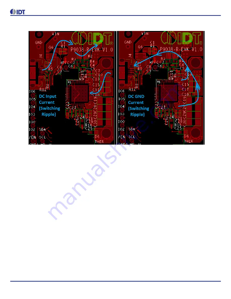
Figure 7. P9038 Recommended Placement and Top Layer Routing of Full-Bridge Inverter and Resonance
Tank with DC (+ripple(GND Bounce)) Current Path Shown
Inspection of
shows how the main power input power rail is routed on the P9038-R-EVK. It is recommended to keep
the SW1 and SW2 signals on the same physical side of the PCB as the P9038 and make VIN switch layers since the SW1/2
signals are AC and more sensitive to vias and layer transfers than the relatively stable (DC + ripple) VIN current.
The connections from the IN caps to IN and PGND pins plus the SW1 and SW2 nodes should be considered capable of radiating
EMI and these should not be allowed to become excessively long (more than 6” (15cm) to either the inductor or resonance
capacitors. If these connections must be longer, it is recommended that they are coupled with a GND plane. The P9038 design
was implemented with optimal EMI performance in mind; therefore, EMI should be acceptable with plenty of margin to pass EMI
compliance testing without the need for additional layout considerations.
BST and ZVS Capacitors
BST1 capacitor C10 and BST2 capacitor C21 should be placed immediately outside the PGND connections and in direct contact
with the SW1 and SW2 nodes, respectively. The key to properly placing and connecting these capacitors is to keep the
connections from the BSTx pins to the respective switch nodes short and low inductance (15 – 20 mils wide and use 2 vias if
layer transitions are necessary). The BST1 and BST2 capacitors should always be close to the P9038 device.
The ZVS components, C7 for SW1 node and C28 for SW2 node, are ideally placed near the P9038 device and will be routed
around the BST1 & BST2 connections to the respective PGND pins. Maintaining symmetry between the two switching nodes is
recommended to achieve optimal performance.
By inspecting the
, notice should be taken of the short direct path C10 and C21 have to the SW1 and SW2 nodes and
the way the trace length expands as the connection escapes from the P9038 device. This reduces the inductance of this
connection, which insures full and fast saturation of the gates of the high side switches at the appropriate time for the FETs to
switch. Then the ZVS components are placed and they are routed around the BST1 and BST2 capacitors.


