08/23/15
13
P9038 LAYOUT GUIDE
AN-894
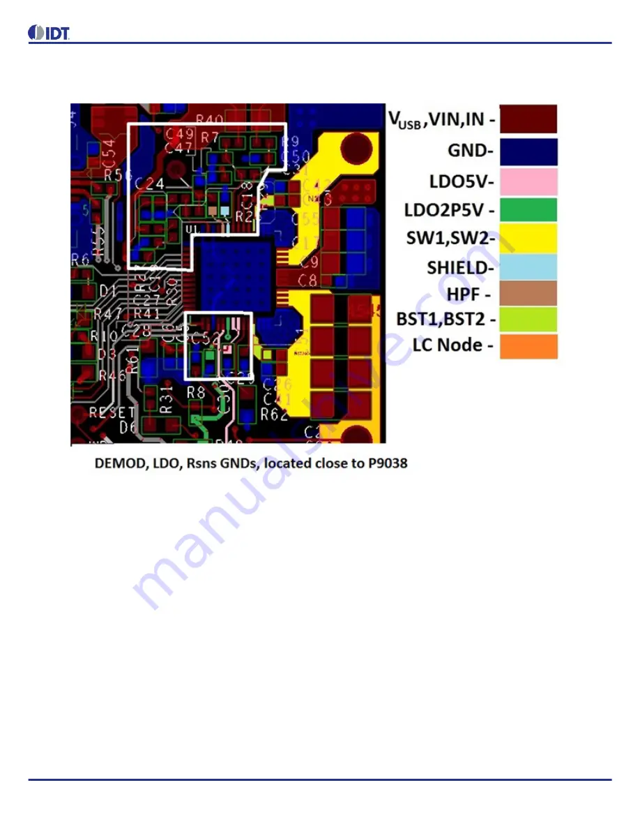
Figure 11. Sensitive DEMOD, Rsns Filter, LDO GND Located on opposite side of the P9038 from the PGND
pins. Provide GND connection directly to EPAD for these GNDs.
The current sense connections from R2 to R3 and R4 are done in a Kelvin manner, directly to the pins of R2. This is done to get
the most accurate voltage drop across the sense resistor prior to filtering and amplification by the internal differential amplifier
used to help calculate input power for FOD.
Non-sensitive Circuits
The remaining components and pins that have not been mentioned are regarded as non-sensitive circuits. The placement and
routing of these nodes is not considered critical to performance or functionality, and so they simply need to be present and
properly connected. In most cases, 6 mil wide traces and any method of connectivity will suffice to complete the circuit.
PCB Footprint Design
PCB Footprint can have a substantial impact on reliability and production yield. In order to avoid placement and soldering issues
during assembly and product deployment, it is recommended to allow sufficient copper landing pads to be exposed, utilize
soldermask, and apply a proper amount of solder paste to the IC. Furthermore, PCB cleaning is highly recommended after the
reflow process is completed.
The P9038 datasheet should be referenced during footprint design, and the following image provides some additional landing
pad allowance and soldermasking recommendations. The exposed pin (etch) used to solder the IC to the PCB must be at least
as large as the physical pin of the package. It is highly recommended to add some additional length (L) to each pin to promote
proper soldering. It is imperative to include soldermask around each pin in order to eliminate potential solder shorts during
assembly and reflow. It is also not suggested to pour continuous copper planes in the pin area. Instead, use a small trace to
connect pins to the planes.


