background image

10

REVISION   C   09/29/14

82P33731/33831 EVALUATION BOARD  

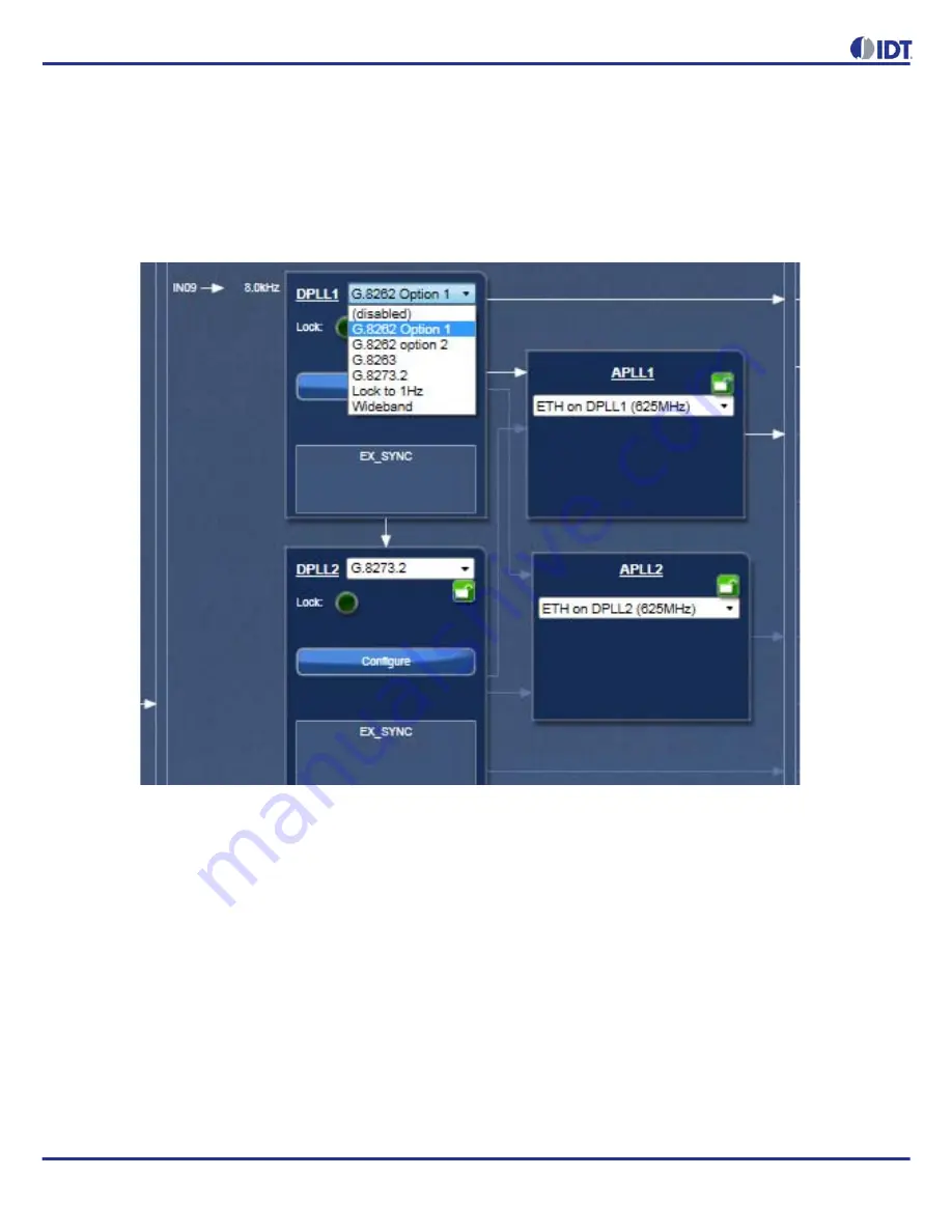
G.8273.2: to configure the DPLL for T-BC (Telecom Boundary Clock), which occurs when a IEEE-1588 stack is 

directly controlling the DCO with phase offsets. It also puts the DPLL in combo mode to synchronize to the other PLL 
running G.8262-Option 1 profile

Lock to 1Hz: to configure the DPLL for GPS application and locking to 1PPS only

Wideband: to configure the DPLL to operate in line card mode or lock to a 10MHz + 1PPS from GPS 

Figure 9. Frequency Profiles for DPLL1

Click “Configure” button to open up configuration window for respective DPLL for additional or customized configuration. 
There are pull-down items for each configuration parameter. For example, in “Operation Mode” section, you can select:

Automatic, or Free-up to force Lock or Free-run;

Different base frequencies can be selected from pull-down items in Selector A or Select B;

Input reference can be set manually set to a particular input, or set it in “Automatic” mode, in which case a input 

reference is selected based on priority among multiple input references;

Feedback can be “Internal feedback mode” or use one of the input references as an “external feedback mode”. When 

in external feedback mode, a clock source must be supplied to the input chosen at the same frequency as the input 
to the DPLL (typically, it's 8kHz).

Summary of Contents for 82P33731

Page 1: ...Output SMA Connectors There are a total of 12 outputs of which OUT1 2 7 9 10 are single ended outputs OUT3 4 5 6 11 12 are differential outputs OUT8 is an AMI output USB connector Type B connector for...

Page 2: ...e from OSCI or XO Please see board silkscreen for source selection Dip Switch SW5 This dip switch contains the following bit configurations System clock frequency selection switch the 3 bits to match...

Page 3: ...se them to power the board They are connected to the output of 3 3V and 1 8V voltage regulators powered by either J54 or the 5VDC power jack They can be supplied with 3 3V and 1 8V to power the board...

Page 4: ...ult frequencies will be available OUT1 25MHz OUT2 125MHz OUT3 156 25MHz FRSYNC 8kHz MFRSYNC 2kHz Working with TimingCommand for Configuration Use the following steps to start the configuration of the...

Page 5: ...ck the button at the lower right corner of the window to browse and select the correct personality file then click OK Note Due to the hardware structure of the chip two personality files will need to...

Page 6: ...window In the center of the window DPLL1 3 and APLL1 3 are displayed Each DPLL can be individually configured see Step 6 below APLL1 and APLL2 each has pull down menu to choose different base frequen...

Page 7: ...nput Right Output Center Device Block Diagram 5 For Input configuration most frequencies can be entered for IN01 IN14 and they will be automatically configured to be available to both DPLLs For each f...

Page 8: ...and Output Frequencies To associate an input clock i e IN09 with a sync signal such as 1PPS click on the Input Buffer of IN09 the triangle symbol following frequency entry box a sub configuration win...

Page 9: ...tion and a Configure button In general the pull down Profile Selection should be sufficient to automatically pre configure the DPLL and reference monitor for the specific ITU T recommendation Frequenc...

Page 10: ...ion window for respective DPLL for additional or customized configuration There are pull down items for each configuration parameter For example in Operation Mode section you can select Automatic or F...

Page 11: ...elect DPLL s bandwidth and damping factors during start acquisition and locked phases Always use Locked bandwidth damping this option will use the bandwidth and damping factor that are available when...

Page 12: ...ed However 19 2MHz and 10MHz based clocks are not supported by the default hardware profiles for the APLLs Therefore APLL1 APLL2 needs to be pre configured to the applicable VCO frequency To configure...

Page 13: ...as shown in Figure 12 Then click on Customize button and ignore the initial Timing Commander error Enter the values as shown in Figure 14 below Figure 14 Configure APLL2 Parameters for VCO 600 0MHz On...

Page 14: ...r desired output frequencies in OUT11 and or OUT12 Only OUT11 and OUT12 are from APLL3 Please see portion of the window configuring APLL3 in Figure 16 below Writing to APLL3 related registers requires...

Page 15: ...SYNC and MRFRSYNC 8 Connecting to the Board GUI Configurations can be made before making the USB I2C connection to the board Alternatively USB connection to the board can be established before TimingC...

Page 16: ...the feature is turned off changes in configurations will be written to the chip by clicking on Writing all registers to the chip button 9 Writing to APLL3 related registers The step described above wi...

Page 17: ...to APLL3 related Registers 10 Viewing Status After writing all registers with configured input reference clocks available the PLL is supposed to lock to the reference clock The PLL operation status c...

Page 18: ...18 REVISION C 09 29 14 82P33731 33831 EVALUATION BOARD Figure 22 DPLL Status Window...

Page 19: ...REVISION C 09 29 14 19 82P33731 33831EVALUATIONBOARD Board Schematics Figure 23 82P33x31 Evaluation Board Schematics Page 1 Block Diagram...

Page 20: ...20 REVISION C 09 29 14 82P33731 33831 EVALUATION BOARD Figure 24 82P33x31 Evaluation Board Schematics Page 2 Reference Selection...

Page 21: ...REVISION C 09 29 14 21 82P33731 33831EVALUATIONBOARD Figure 25 82P33x31 Evaluation Board Schematics Page 3 I O Termination...

Page 22: ...22 REVISION C 09 29 14 82P33731 33831 EVALUATION BOARD Figure 26 82P33x31 Evaluation Board Schematics Page 4 Control...

Page 23: ...REVISION C 09 29 14 23 82P33731 33831EVALUATIONBOARD Figure 27 82P33x31 Evaluation Board Schematics Page 5 Power...

Page 24: ...sented only as a guide and does not convey any license under intellectual property rights of IDT or any third parties IDT s products are not intended for use in applications involving extreme environm...

Reviews: