PCI-DIO48(S)(S) Manual
Page 6-2
Manual 00650-529-1
Each PPI contains a Control Register. This write-only, 8-bit register is used to set the mode and
direction of the groups. At Power-Up or Reset, all I/O lines are set as inputs. Each PPI should be
configured during initialization by writing to the Control Registers even if the groups are only
going to be used as inputs. Output buffers are automatically set by hardware according to the
Control Register states. Note that Control Registers are located at base a3 and base
a7. Bit assignments in each of these Control Registers are as follows:
Bit
Assignment
Code
D0
Port C Lo (C0-C3)
1=Input, 0=Output
D1
Port B
1=Input, 0=Output
D2
Mode Select
1=Mode 1, 0=Mode 0
D3
Port C Hi (C4-C7)
1=Input, 0=Output
D4
Port A
1=Input, 0=Output
D5,D6
Mode Select
00=Mode 0, 01=Mode 1, 1x=Mode 2
D7
Mode Set Flag
1=Active
Table 6-2:
Control Register Bit Assignment
Note
Mode 1 cannot be used by these cards without modification. Thus, bits D2, D5, and D6 should
always be set to "0". If your card has been modified to operate in Mode 1, then there will be an
Addendum page in the front of this manual. These cards cannot be used in Mode 2 of the PPI.
Note
In Mode 0, do not use the control register byte for the individual bit control feature. The hardware
uses the I/O bits to control buffer direction on this card. The control register should only be used
for setting up input and output of the ports and enabling the buffer.
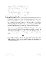
These cards provide a means to enable/disable the tristate I/O buffers under program control. If
the TST/BEN jumper on the card is installed in the BEN position, the I/O buffers are permanently
enabled. However, if that jumper is in the TST position, enable/disable of the buffers is software
controlled via the control register as follows:


