


4 - 3
4-2-5 APC CIRCUIT
The APC circuit (IC3a, Q37) protects drive and power ampli-
fiers from excessive currents and selects HIGH or LOW out-
put power.
The output voltage from the current detector circuit is applied
to the inverting amplifier (IC3a, pin 2), and the T4/PWR sig-
nal from the CPU (IC8, pins 54–59) is applied to the other
input for reference.
When the driving current increases, the input voltage of the
differential amplifier (Q9, pin 1) will be decreased. In such
cases, input voltage of the inverting amplifier (pin 2) is
increased to decrease the output power.
Q37 is controlled by the TXC signal from the CPU (IC8, pin
50) to select HIGH or LOW output power.
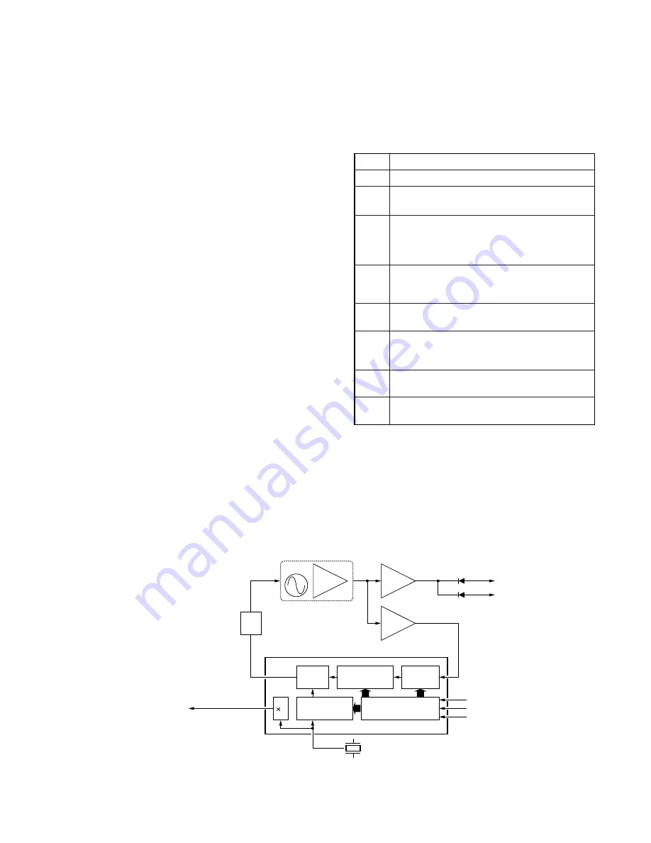
4-3 PLL CIRCUIT
A PLL circuit provides stable oscillation of the transmit fre-
quency and receive 1st LO frequency. The PLL output com-
pares the phase of the divided VCO frequency to the refer-
ence frequency. The PLL output frequency is controlled by
the divided ratio (N-data) of a programmable divider.
The PLL circuit contains the VCO circuit (Q7, Q8, D6). The
oscillated signal is amplified at the buffer-amplifiers (Q5, Q6)
and then applied to the PLL IC (IC1, pin 2).
The PLL IC contains a prescaler, programmable counter, pro-
grammable divider, phase detector and charge pump, etc.
The entered signal is divided at the prescaler and program-
mable counter section by the N-data ratio from the CPU. The
divided signal is detected on phase at the phase detector
using the reference frequency.
If the oscillated signal drifts, its phase changes from the ref-
erence frequency, causing a lock voltage change to compen-
sate for the drift in the oscillated frequency.
A portion of the VCO signal is amplified at the buffer-amplifi-
er (Q4, Q6) and is then applied to the receive 1st mixer or
transmit buffer-amplifier circuit via the T/R switching diode
(D3, D4).
4-4 POWER SUPPLY CIRCUITS
VOLTAGE LINE
Description
The voltage from the attached battery pack/case.
The same voltage as the BATT line controlled by
the [PWR/VOL] control.
Common 5 V converted from the VCC line by the
reference regulator circuit (IC6). The output volt-
age is applied to the CPU (IC8) and the 5V regu-
lator circuit, etc.
Common 5 V converted from the VCC line at the
5 V regulator circuit (Q18, Q19) using the CPU5
line voltage for reference.
Transmit 5 V converted from the VCC line at the
T5 regulator circuit (Q22, Q40).
Receive 5 V converted from the 5 V line at the R5
regulator circuit (Q21). The regulated voltage is
applied to the receiver circuits.
Common 5 V converted from the 5V line by the S5
regulator circuit (Q20).
The same voltage as the 5V line for the optional
HM-75A or HS-51 through a resistor (R132).
Line
BATT
VCC
CPU5
5V
T5
R5
S5
OPT
• PLL circuit
Shift register
2
Prescaler
Phase
detector
Loop
filter
Programmable
counter
Programmable
divider
X1
15.2 MHz
30.4 MHz signal
to the FM IF IC
16
Q7, Q8
VCO board
Buffer
Q6
Buffer
Q4
Buffer
Q5
3
4
5
PLST
SCK
SO
to transmitter circuit
to 1st mixer circuit
D4
D3
17
8
2


