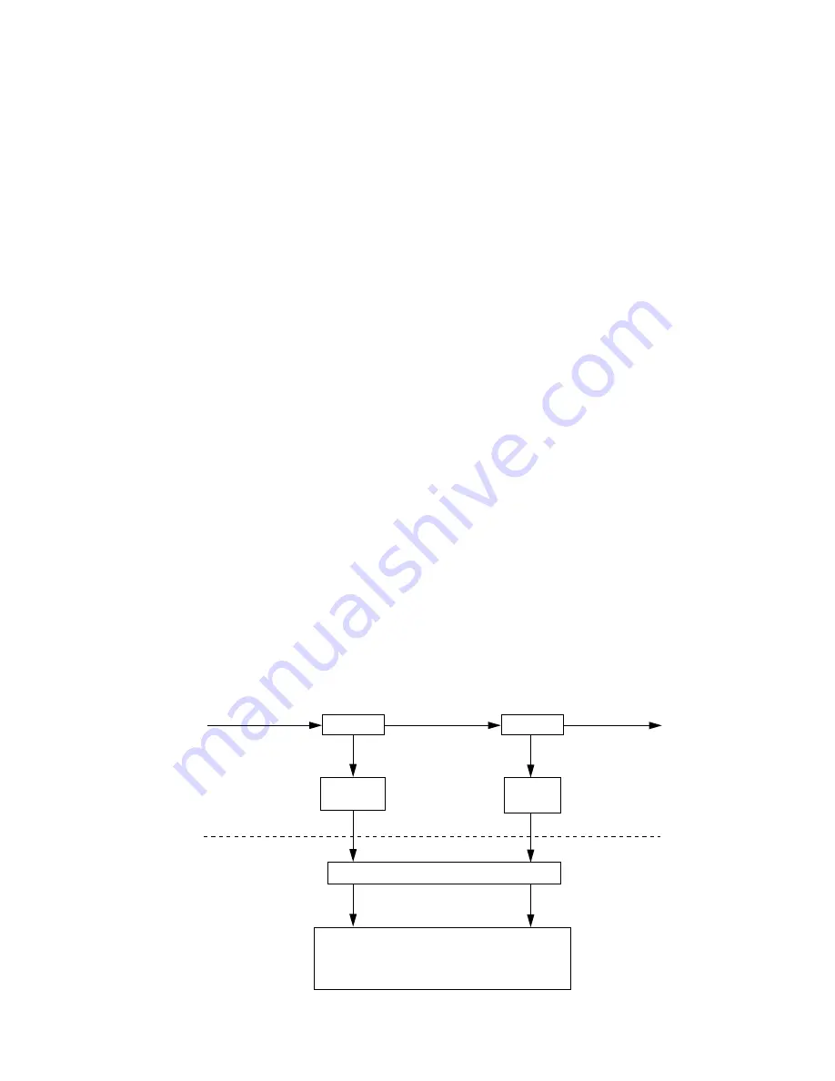
3 - 2
2-step (3-step for the 50 MHz band) Chebyschev low-pass
filters are adopted, to obtain –60 dB or less higher harmon-
ic emissions for all HF bands or –70 dB or less for the 50
MHz band.
The filtered signal is passed through or bypasses the anten-
na tuner and is then applied to one of four antenna connec-
tors via the antenna select relay (RL1–RL4) on the ANT-SW
unit.
3-2 ANTENNA TUNER CIRCUITS
3-2-1 MATCHING CIRCUIT (TUNER UNIT)
The matching circuit is a T-network. Using 2 tuning motors,
the matching circuit obtains rapid overall tuning speed.
Using relays (TUNER unit; RL1–RL10, L-NET board; RL1,
RL2, H-NET board; RL1–RL10), the relay control signals
from the antenna tuner CPU (MAIN unit; IC12) via the relay
driver (MAIN unit; IC14) ground one of the taps of L3–L5 (L-
NET board) or L11–L15 (H-NET board) and add network
capacitors (C-NET board). After selecting the coils and
capacitors, 2 motors (TUNER unit; MF1, MF2) adjust C1
and C2 using the antenna tuner CPU and the motor driver
(MAIN unit; IC15) to obtain a low SWR (Standing Wave
Ratio).
3-2-2 DETECTOR CIRCUIT
(MAIN AND FILTER UNITS)
(1) SWR DETECTOR
Forward and reflected power are picked up by a current
transformer (FILTER unit; L22), detected by D15 and D16,
and then applied to the MAIN unit.
The applied signals are amplified at the SWR amplifier
(MAIN unit; IC31a/b). The amplified voltages are applied to
the antenna tuner CPU (MAIN unit; IC12, pins 2, 3). The
CPU detects the SWR.
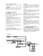
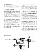
(2) REACTANCE COMPONENTS DETECTOR
Reactance components are picked up by comparing the
phase of the RF current and RF voltage. The RF current is
detected by L3 and R4 (DET board), and then amplified at
IC1a and IC2d. The amplified RF current is applied to the
phase comparator (DET board; IC4, pin 13). The RF volt-
ages are detected at C1–C3 on the DET board, and ampli-
fied at IC1c and IC2a, then applied to the phase comparator
(IC4, pin 1). The output signal from the phase comparator
(IC4, pin 6 for RF voltage, pin 9 for RF current) is rectified at
D13 and D14 for conversion into DC voltage. The rectified
voltage signals are combined, then applied to the antenna
CPU (MAIN unit; IC12, pin 64) after being amplified at IC9a
on the MAIN unit.
ECL-IC is used for IC1 and IC2 on the DET board to ensure
quick and stable signal detection even at low RF signal level
input.
(3) RESISTANCE COMPONENTS DETECTOR
Resistance components are picked up by L5, R14 and R21,
and detected by Q1, D11 and D12 on the DET board. The
detected resistance components are amplified at IC9a on
the MAIN unit, and then applied to the antenna CPU (IC12,
pin 1).
3-2-3 MOTOR CONTROL CIRCUIT
(MAIN UNIT AND C-NET, L-NET, H-NET
BOARDS)
The control circuit of the internal antenna tuner consists of
the CPU, EEPROM, tuning motors and tuning relays.
(1) CPU AND EEPROM (MAIN UNIT)
The antenna tuner CPU (IC12) controls the tuning motors
via the motor driver (IC15) and tuning relays via the relay dri-
ver (IC14, Q9–Q14). The CPU memorizes the best preset
position and the contents are stored in the EEPROM (IC7)
without the need for a backup battery.
• DETECTOR CIRCUIT
COUPLER
COUPLER
L3, R4
L5, R14, R21
Impedance
detector
Phase
detector
Q1, D11,
D12
D3, D4,
D5, D6,
D13, D14,
IC2, IC4
IC9
Tuner CPU
IC12
64
1
From FILTER unit
To C-NET board
DET board
MAIN unit
6
7
1
2
Amplifier
Summary of Contents for IC-PW1
Page 1: ...SERVICE MANUAL ADDENDUM CONTENTS PARTS LIST 1 BOARD LAYOUTS 16 VOLTAGE DIAGRAM 18 Mar 2011 ...
Page 24: ...SERVICE MANUAL ADDENDUM CONTENTS PARTS LIST 1 BOARD LAYOUTS 16 Jun 2010 ...
Page 42: ...SERVICE MANUAL ADDENDUM CONTENTS PARTS LIST 1 BOARD LAYOUTS 16 VOLTAGE DIAGRAM 18 Apr 2010 ...
Page 96: ...HF 50 MHz ALL BAND LINEAR AMPLIFIER iC PW1 ...
Page 175: ...MNF F1 EP2 TO REGRELAY BOARD MLF EP1 F2 TO REGRELAY BOARD EP35 I N FG 8 19 FIL AC BOARD 8 20 ...
Page 201: ...A 5449MZ S 3 1999 Icom Inc 1 1 32 Kamiminami Hirano ku Osaka 547 0003 Japan Count on us ...


