Icom IC-GM1600, Service Manual
The Icom IC-GM1600 is a reliable and efficient communication device designed for marine use. This compact and durable handheld radio ensures reliable communication at sea. For an in-depth understanding of its features and operation, you can easily download the free Instruction Manual from our website, manualshive.com.
Share
Download


Reviews:
No comments
Related manuals for IC-GM1600
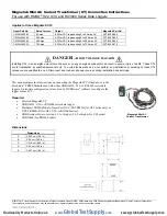
CT
Brand: MAGNELAB Pages: 2

Beolab transmitter 1
Brand: Bang & Olufsen Pages: 30

LC2
Brand: M-system Pages: 3

SCX 2,4 GHz
Brand: Jamara Pages: 8

DMR 61
Brand: JAMO Pages: 18

DVR 50
Brand: JAMO Pages: 17

DMR 45
Brand: JAMO Pages: 1

VOS-8040FDMR
Brand: Voscom Pages: 15

ROP-03
Brand: Zamel Pages: 4

gAirHawk
Brand: GEOSUN Pages: 9

GDL 52
Brand: Garmin Pages: 41

RC.8
Brand: Radio Corporation Pty Pages: 75

Efector 600 TADx91 Series
Brand: IFM Electronic Pages: 25

WP3W-RK
Brand: IDT Pages: 25

D58-4
Brand: HobbyKing Pages: 2

B.RO 44 Series
Brand: Allmatic Pages: 10

EX-1441
Brand: Exsys Pages: 2

L88
Brand: Dynascan Pages: 10


