background image

4 - 2

(3) 76.0 MHz–229.995 MHz RF CIRCUIT
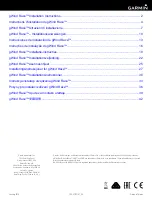
The signals from the antenna switching circuit pass through
the attenuator (D351), and then applied to the bandpass fil-
ter (D352, D353, L351, L352) to suppress unwanted signals.
The signals pass through the bandpass filter (D354–D356,
D359, L354, L355, L357, L358, C357–C364) after being
amplified at the RF amplifier (Q351).

(4) 230.0 MHz–629.995 MHz RF CIRCUIT
The signals from the antenna switching circuit are applied to
the band switch (D457), and then pass through the attenua-
tor (D401). The signals pass through the bandpass filter
(D402, D403, L401, L402, C402, C404–C406) to suppress
unwanted signals, then applied to the RF amplifier (Q401).
The amplified signals pass through the bandpass filter
(D405, D407, L409, C414, C415), and are then amplified at
the RF amplifier (Q402).

(5) 630.0 MHz–999.990 MHz RF CIRCUIT
The signals from the antenna pass through the high-pass fil-
ter (L3, L4, C6–C8), and then applied to the attenuator
(D451) after being passed through the band switch (D10).
The signals pass through the bandpass filter (D452, L451,
C451–C454), then applied to the RF amplifier (Q451). The
amplified signals pass through the bandpass filter (D453,
D454, L452, L453, C456, C460, C462–C464) and RF ampli-
fier (Q452).

The amplified or filtered signals pass through one of the band
switch (D303, D313, D358, D408, D455), and then applied to
the 1st mixer circuit (IC351, pin 1).

4-1-4 1ST MIXER AND 1ST IF CIRCUITS (RF, AF

AND VCO UNITS)

The 1st mixer circuit converts the received RF signals to a
fixed frequency of the 1st IF signal with a PLL output fre-
quency. By changing the PLL frequency, only the desired fre-
quency will pass through the bandpass filter at the next stage
of the 1st mixer.

The amplified or filtered RF signals are mixed with 1st LO
signals at the 1st mixer (IC351) to produce a 69.45 MHz 1st
IF signal. The 1st IF signal is output from pin 6, and passed
through the bandpass filter (Narrow: AF unit; FI101, Wide: AF
unit; FI102) to suppress unwanted harmonic components via
the mode switch (AF unit; D101, D102). The filtered 1st IF
signal is applied to the IF amplifier (AF unit; Q102). The
amplified signal is applied to the 2nd mixer circuit.

The 1st LO signals (53.350 MHz–99.345 MHz, 99.350
MHz–560.545 MHz or 281.675 MHz–534.720 MHz) are gen-
erated at the 144 MHz VCO (VCO unit; Q3–Q5, D3, D4) or
430 MHz VCO (VCO unit; Q1, Q2, D1) circuits. The oscillat-
ed signal is applied to the 1st mixer via the doubler circuit
(Q354, D357) or directly.

4-1-5 2ND IF AND DEMODULATOR CIRCUITS

(AF UNIT)

The 2nd mixer circuit converts the 1st IF signal to a 2nd IF
signal. A double conversion superheterodyne system (which
converts receive signals twice) improves the image rejection
ratio and obtain stable receiver gain.

The FM IF IC (IC151) contains 2nd local oscillator, 2nd mixer,
limiter amplifier, quadrature detector and S-meter detector
circuits.

The amplified 69.45 MHz 1st IF signal from the IF amplifier
(Q102) is mixed with the 2nd LO signal at the 2nd mixer
(IC151) to produce a 455 kHz 2nd IF signal. The 2nd IF sig-
nal from the IC151, pin 3 passes through (AM and FM mode)
or bypasses (WFM mode) the 2nd IF filter (FI151) where
unwanted heterodyne signals are suppressed via the mode
switch (D151, D152). The filtered signals are applied to the
AM detector circuit or FM detector circuit respectively.

RF

RF

SW

SW

SW

BPF

BPF

BPF

RF

SW

BPF

BPF

RF

RF

SW

BPF

BPF

RF

RF

SW

BPF

BPF

0.495 MHz  75.995 MHz
RF signals

1st LO signal
from the VCO circuit

Q401

Q451

Q402

Q452

Q351

Q302

D303

D313

D358

D408

D455

D301,
D306

Q303

1st mixer

(IC351)

1st IF signal to the AF unit
(AM, FM: 69.45 MHz,
WFM: 13.35 MHz)

76.0 MHz  299.995 MHz
RF signals

230.0 MHz 629.995 MHz
RF signals

630.0 MHz  999.990 MHz
RF signals

"AGC" signal from
the AF unit (Q202, pin 4)

• RF CIRCUIT

Summary of Contents for IC-E90

Page 1: ...S 13903MZ C2 2002 Icom Inc 1 1 32 Kamiminami Hirano ku Osaka 547 0003 Japan MULTIBAND FM TRANSCEIVER ie90 ic e90 IC E90 1 4...

Page 2: ...replacement parts 1 10 digit order numbers 2 Component part number and name 3 Equipment model name and unit name 4 Quantity required SAMPLE ORDER 1130006220 S IC TC4W53FU IC E90 LOGIC UNIT 1 piece 893...

Page 3: ...4 4 POWER SUPPLY CIRCUITS 4 7 4 5 PORT ALLOCATIONS 4 7 SECTION 5 ADJUSTMENT PROCEDURES 5 1 PREPARATION 5 1 5 2 TRIMMER ADJUSTMENT 5 3 5 3 ADJUSTMENT MODE ADJUSTMENTS 5 5 SECTION 6 PARTS LIST SECTION 7...

Page 4: ...ns projections not included 58 W 87 H 29 D mm 217 32 W 37 16 H 15 32 D in Weight with BP 217 Ant 280 g 97 8 oz M TRANSMITTER Output power at 8 0 V DC High 5 0 W typical Low 0 5 W typical Modulation sy...

Page 5: ...D AM is mea sured at 10 dB S N 2 The frequency range is between 222 000 MHz and 229 995 MHz 3 The frequency range is between 320 000 MHz and 330 000 MHz 4 The frequency range is between 40 000 MHz and...

Page 6: ...or Q201 2SB1201 Q202 XP1501 3 regulator Q8 2SB1132 Q9 XP1501 3C regulator Q142 XP1501 Q145 2SB1132 D143 MA2S111 CPU3 regulator IC141 NJM2370U32 440 MHz band modulation switch Q304 2SJ364 Microphone mu...

Page 7: ...Q452 2SK3475 T3 regulator Q56 XP4315 D50 MA6S121 1st mixer IC351 PC2757TB VCO circuit Power amplifier Q51 2SK3476 FM IF IC IC151 TA31136FN 1st AF amplifier Q205 2SD2216 AF mute Q251 2SJ364 IF amplifie...

Page 8: ...unit NOTE When you tighten 6 screws E tighten those in turn of 1 6 q Take off the lock plate w Unsolder 5 points F at the antenna plate vol plate and lead e Unscrew 1 screw G 2 4 mm silver and 2 screw...

Page 9: ...ls are applied to the each antenna switching circuit RF signals 0 495 MHz 75 995 MHz The signals pass through the antenna switching circuit D9 and then applied to the RF circuit RF signals 76 0 MHz 29...

Page 10: ...he 1st mixer IC351 to produce a 69 45 MHz 1st IF signal The 1st IF signal is output from pin 6 and passed through the bandpass filter Narrow AF unit FI101 Wide AF unit FI102 to suppress unwanted harmo...

Page 11: ...for the CTCSS squelch detection via the CTCIN line The electronic volume control circuit controls AF gain there fore the AF output level is according to the VOL setting and also the squelch conditions...

Page 12: ...4 2 3 DRIVE POWER AMPLIFIER CIRCUITS RF UNIT The drive amplifier circuit amplifies the transmit signal to a level needed for the power amplifier circuit The power ampli fier circuit amplifies this to...

Page 13: ...riving current 4 3 PLL CIRCUITS 4 3 1 GENERAL A PLL circuit provides stable oscillation of the transmit fre quency and the receive local frequency The PLL circuit compares the phase of the divided VCO...

Page 14: ...D7 D8 When the signal is applied to the divider circuit IC1 pin 2 the circuit divides the VCO signal into the ratio of 1 2 The divided signal passes through the low pass filter L12 L13 C48 C51 and div...

Page 15: ...ted from the 3 line by the T3 regulator circuit RF unit Q56 and D20 The output voltage is applied to the buffer amplifier RF unit IC51 pin 6 4 4 POWER SUPPLY CIRCUITS VOLTAGE LINE Pin Port Description...

Page 16: ...Outputs the R3C regulator control sig nal Low While receiving Outputs the T5V regulator control sig nal High While transmitting 46 47 48 49 51 52 53 54 55 56 57 58 61 62 65 66 69 70 71 72 73 74 75 77...

Page 17: ...selected Outputs the DTCS decorder filter con trol signal Output segment data to the LCD LOGIC unit DS4 pins 5 7 Outputs segment data to the LCD LOGIC unit DS4 pin 8 Output segment data to the LCD LO...

Page 18: ...el indicator as follow EQUIPMENT DC power supply RF power meter terminated type Frequency counter FM deviation meter GRADE AND RANGE Output voltage 11 V DC Current capacity 3 A or more Measuring range...

Page 19: ...dB or 50 dB FM deviation meter Standard signal generator 0 1 V to 32 mV 127 dBm to 17 dBm Audio generator CAUTION DO NOT transmit while an SSG is connected to the antenna connector Optional SMA BNC ad...

Page 20: ...WFM Receiving Displayed frequency 629 990 MHz Mode FM Receiving Displayed frequency 144 000 MHz Transmitting Displayed frequency 148 000 MHz Transmitting Displayed frequency 440 000 MHz Transmitting D...

Page 21: ...5 4 CP PLL lock voltage check point L456 L16 TX power balance adjustment 435 MHz L19 TX power balance adjustment 145 MHz VCO UNIT RF UNIT...

Page 22: ...PH ch 440 000 MHz Output power High Transmitting Displayed frequency PH ch 450 000 MHz Transmitting Displayed frequency PH ch 50 000 MHz Output power Low Transmitting Displayed frequency PH ch 53 900...

Page 23: ...0 000 MHz Output power High Transmitting Displayed frequency PL ch 53 900 MHz Transmitting Displayed frequency PL ch 144 000 MHz Output power High Transmitting Displayed frequency PL ch 148 000 MHz Tr...

Page 24: ...requency DL ch 440 000 MHz Output power Low Transmitting Set the channel indicator PL Transmitting Set the channel indicator DL Transmitting Displayed frequency DL ch 450 000 MHz Output power Low Tran...

Page 25: ...equency DE ch 440 000 MHz Output power Low Transmitting Set the channel indicator PE transmitting Set the channel indicator DE Transmitting Displayed frequency DE ch 450 000 MHz Output power Low Trans...

Page 26: ...MHz Transmitting Displayed frequency DH ch 440 000 MHz Transmitting Displayed frequency DM ch 52 000 MHz No audio applied to the MIC jack Set an FM deviation meter as HPF OFF LPF 20 kHz De emphasis OF...

Page 27: ...itting Displayed frequency CT ch 145 000 MHz Transmitting Displayed frequency CT ch 445 500 MHz Transmitting Displayed frequency DS ch 51 000 MHz No audio applied to the MIC jack Set an FM deviation m...

Page 28: ...ng Displayed frequency TH ch 75 100 MHz A Set the SSG as Level 1 V 107 dBm Receiving Displayed frequency TL ch 76 100 MHz B Set the SSG as Level 1 V 107 dBm Receiving Displayed frequency TH ch 149 100...

Page 29: ...IC151 pin 12 SD line RF Tracking check point L151 Detector coil adjustment CP0 Detector coil check point NOTE A EUR ITR UK only B except ESP 5 12 AF UNIT...

Page 30: ...H ch 900 100 MHz A Set the SSG as Level 3 2 V 97 dBm Receiving AF Connect a DC volt meter or oscillo scope to the IC151 pin 12 SD line Maximum voltage Maximum voltage Maximum voltage Maximum voltage M...

Page 31: ...odes When adjust the WFM mode set the SSG s deviation as 52 5 kHz Push the BAND key Push the BAND key This output level of the standard signal generator SSG is indicated as SSG s open circuit IC151 pi...

Page 32: ...DIODE MA2S077 TX D405 1720000790 S VARICAP HVC321B1TRF D406 1790001260 S DIODE MA2S077 TX D407 1720000790 S VARICAP HVC321B1TRF D408 1750000800 S DIODE HVC136TRF D451 1790001160 S DIODE 1SS362 TE85R...

Page 33: ...RJ2GEJ 220 X 22 R358 7030005090 S RESISTOR ERJ2GEJ 104 X 100 k R359 7030005090 S RESISTOR ERJ2GEJ 104 X 100 k R360 7030005040 S RESISTOR ERJ2GEJ 472 X 4 7 k REF ORDER DESCRIPTION NO NO RF UNIT R361 70...

Page 34: ...0 S CERAMIC ECJ0EB1E102K C352 4030017380 S CERAMIC ECJ0EC1H050B C353 4030017460 S CERAMIC ECJ0EB1E102K 6 3 REF ORDER DESCRIPTION NO NO RF UNIT C354 4030017460 S CERAMIC ECJ0EB1E102K C355 4030017460 S...

Page 35: ...RESISTOR ERJ2GEJ 104 X 100 k R3 7030005090 S RESISTOR ERJ2GEJ 104 X 100 k R4 7030006610 S RESISTOR ERJ2GEJ 394 X 390 k R5 7030004970 S RESISTOR ERJ2GEJ 470 X 47 R7 7030005120 S RESISTOR ERJ2GEJ 102 X...

Page 36: ...MIC ECJ0EB1C103K C154 4030017670 S CERAMIC ECJ0EC1H390J C155 4030017700 S CERAMIC ECJ0EC1H151J C156 4030017460 S CERAMIC ECJ0EB1E102K 6 5 REF ORDER DESCRIPTION NO NO AF UNIT C157 4030017460 S CERAMIC...

Page 37: ...2 TE85R D301 1790001560 S DIODE 1SS372 TE85R D302 1790001560 S DIODE 1SS372 TE85R X1 6050011080 S XTAL CR 687 6 7584 MHz L24 6200003640 S COIL MLF1608E 100K T L140 6200003640 S COIL MLF1608E 100K T R1...

Page 38: ...7030005170 S RESISTOR ERJ2GEJ 474 X 470 k R368 7030005170 S RESISTOR ERJ2GEJ 474 X 470 k R400 7030005090 S RESISTOR ERJ2GEJ 104 X 100 k R451 7030008300 S RESISTOR ERJ2GEJ 184 X 180 k R452 7030005600...

Page 39: ...R YG DS12 5040002670 S LED CL 165HR YG MC1 7700002310 MICROPHONE EM 140 S401 2230001090 S SWITCH EVQPSH02K S402 2230001090 S SWITCH EVQPSH02K SP1 2510000840 SPEAKER CS028014 12 REF ORDER DESCRIPTION N...

Page 40: ...S CERAMIC ECJ0EC1H1R5B C17 4030017550 S CERAMIC ECJ0EC1H1R5B C19 4030017730 S CERAMIC ECJ0EB1E471K C20 4030017460 S CERAMIC ECJ0EB1E102K C21 4030017560 S CERAMIC ECJ0EC1H2R5B C22 4030017460 S CERAMIC...

Page 41: ...eet AF 1 MP2 8930058610 Isolating plate HD 1 REF ORDER DESCRIPTION NO NO QTY VCO UNIT MP1 8930056310 2507 terminal holder 1 MP2 8510014590 2507 A VCO case 1 MP5 8410002470 2507 heat sink 1 MP6 8510014...

Page 42: ...C MP26 C MP4 C MP10 C MP9 R MP2 R MP6 R MP1 R MP1 V MP2 V MP2 A MP4 A MP14 R MP15 R W1 L MP21 C MP23 C MP12 R MP13 R MP27 C MP17 C J1 C MP14 C MP28 C MP19 C RF UNIT AF UNIT LOGIC UNIT A B B C C Note C...

Page 43: ...E C E C B E 2SK880 Y XY S D G B E C B E C XP1501 AB 5R B1 E B2 C1 C2 B1 E B2 C1 C2 UN9113 6C B E C XP1214 9H E1 B1 B2 C1 C2 XP4214 BR E1 C2 B1 C1 E2 B2 NAME SYMBOL INSIDE VIEW NAME SYMBOL INSIDE VIEW...

Page 44: ...N VFO MHZ 4 DUP 5 SKIP 6 M N 0 RIT MR S MW 7 TSCAN 8 SET 9 TS DTMF M CALL TV LOCK The combination of this page and the next page shows the unit layout in the same configuration as the actual P C Board...

Page 45: ...VMOD CHG GND 10V WXALT PLSTB WFM TXC DASTB DIUD R3C SD V2C VSFT EXTM MUTE VCC DETO 3 XMOD PATMP GND GND SQL PTT to AF unit J251 SP1 W2 L W2 L The combination of this page and the previous page shows...

Page 46: ...a REF PLSTB CK PDA UL 10V GND VMOD VSHFT CK DATA PLSTB DASTB T43 T50 T14 B4C AGC B1C VCC B5C B3C GND REF PDA UL VMOD HV VSHFT 3 PATMP B2C 10V BSFT V2 FSET V3 V1 IF CHG The combination of this page and...

Page 47: ...The combination of this page and the previous page shows the unit layout in the same configuration as the actual P C Board RF unit BOTTOM VIEW 9 4...

Page 48: ...NTSP GND to LOGIC unit J1 EXT MIC J252 EXT SP REMOTO J253 J251 GND GND PATMP XMOD 3 DETO VCC MUTE EXTM VSHFT V2C SD R3C DIUD DASTB TXC WFM PLSTB WXALT 10V 1 8 1 6 1 8 1 6 to RF UNIT J1 J2 to RF UNIT R...

Page 49: ...nit J251 J51 CK DATA PLSTB DASTB T43 T50 T14 B4C AGC B1C VCC B5 B3 GND REF PDA UL VMOD HV VSHFT 3 PATMP B2C 10V BSFT V2 FSET V3 V1 IF CHG The combination of this page and the previous page shows the u...

Page 50: ...2SD2216 D141 MA2S111 3 HV VCC INTSP VMOD XMOD MUTE DETO REMO 3C TXC DIUD DICK 10V EXTM VOLC VSFT AM WFM BEEP R3C V1C V2C V3C 3 Q146 XP1501 Q147 2SB1132 Q8 2SB1132 Q9 XP1501 Q4 2SB1201 Q10 2SD2216 Q11...

Page 51: ...HVC136 D302 MA2S077 Q302 2SC5006 D303 HVC136 D313 HVC136 D307 MA2S077 D308 HVC321B Q303 2SC5006 D309 MA2S077 D310 HVC321B D352 MA2S077 D353 1SV290 Q351 3SK320 D355 D356 1SV290 D354 D359 MA2S077 D358 H...

Page 52: ...SEG37 6 SEG36 7 SEG35 8 SEG34 9 SEG33 10 SEG32 11 SEG31 12 SEG28 13 SEG27 14 SEG26 15 SEG25 16 SEG24 17 SEG23 18 SEG22 19 SEG21 20 SEG20 21 SEG19 22 SEG18 23 SEG17 24 SEG16 25 SEG15 26 SEG14 27 SEG13...

Page 53: ...A1 2 A2 3 VSS 4 SDA 5 SCL 6 WP 7 VCC 8 W3 R458 47k C102 0 001 C25 0 001 R82 56k C315 0 001 C32 0 001 C240 0 0015 1 2 3 4 5 6 R207 1M R241 330k C17 0 0022 C310 47p C150 0 01 1 2 3 5 CTRL 1 GND 2 NB 3...

Page 54: ...C112 0 001 C88 0 001 L409 18nH R419 3 9k C420 0 01 C421 0 01 1 2 3 4 5 6 MP5 C76 0 01 R77 1k R78 56 R79 56 R80 330 D57 1SV308 C89 0 1 R82 3 9 R81 330 L68 1 0nH L24 65nH D10 1SV308 R11 2 2k R10 2 2k D1...

Page 55: ...O 3 G 4 FL SD BEEP IOSTB PLSTB DASTB 10V PDA UL IF CHG MUTE BEEP BEEP MUTE MUTE VOLC VOLC VOLC HV VMOD PATMP CK R3C DATA XMOD DETO AFV AFV AFV WXALT WXALT REMO INTSP VSHFT AM VCC 3C DETO 3C 3C V3C NOI...

Page 56: ...replacement parts 1 10 digit order numbers 2 Component part number and name 3 Equipment model name and unit name 4 Quantity required SAMPLE ORDER 1130006220 S IC TC4W53FU IC E90 LOGIC UNIT 1 piece 893...

Page 57: ...S 13903MZ C2 2002 Icom Inc 1 1 32 Kamiminami Hirano ku Osaka 547 0003 Japan MULTIBAND FM TRANSCEIVER ie90 ic e90 IC E90 1 4...

Reviews: