Chapter 2. Architecture and technical overview
25
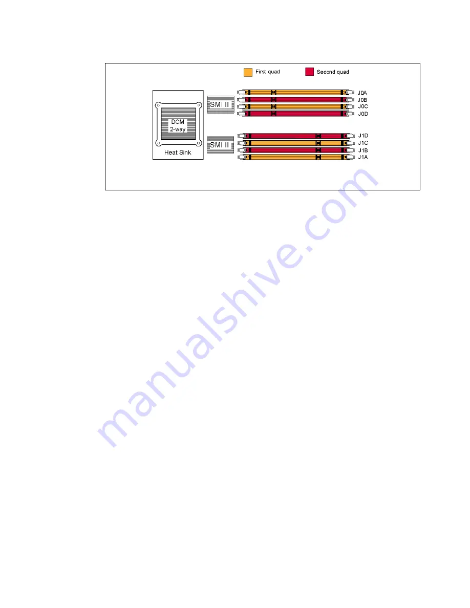
Figure 2-6 Memory placement for the OpenPower 720
2.3.2 Memory throughput
The memory subsystem throughput is based on the speed of the memory, not the speed of
the processor. An elastic interface, contained in the POWER5 chip, buffers reads and writes
to and from memory and the processor. There are two SMIs per processor card, each with a
single 8 byte write and 2 byte read DDR bus to the processor. A DDR bus enables double
read or writes per clock cycle. If 250 MHz memory is installed, the throughput is (16 x 2 x 250)
+ (4 x 2 x 250) or 9.76 GB/second per processor card. If 266 MHz memory is installed the
throughput is (16 x 2 x 266) + (4 x 2 x 266) or 10.41 GB/second. Therefore, a 4-way system
would have a maximum theoretical throughput of 19.53 GB/second using 250 MHz memory
or 20.82 GB/second using 266 MHz memory.
The POWER5 processor’s integrated memory controller further reduces latency over the
previous outboard controller on POWER4 systems to the SMI chips by requiring fewer cycles
in order to set up memory addressing in the hardware.
2.3.3 Memory restrictions
The OpenPower does not officially support OEM memory, and there is no exception to this
rule. OEM memory is never certified for the use in OpenPower servers. If the OpenPower 720
is populated with OEM memory, you could experience unexpected and unpredictable
behavior.
All IBM memory is identified by an IBM logo and a white label printed with a barcode on top
and an alphanumeric string on the bottom, created according to the rule reported in
Figure 2-7.
Summary of Contents for OpenPower 720
Page 2: ......
Page 28: ...18 OpenPower 720 Technical Overview and Introduction...
Page 68: ...58 OpenPower 720 Technical Overview and Introduction...
Page 72: ...62 OpenPower 720 Technical Overview and Introduction...
Page 73: ......


