


FWA6304-D25 Series
User’s
Manual
6
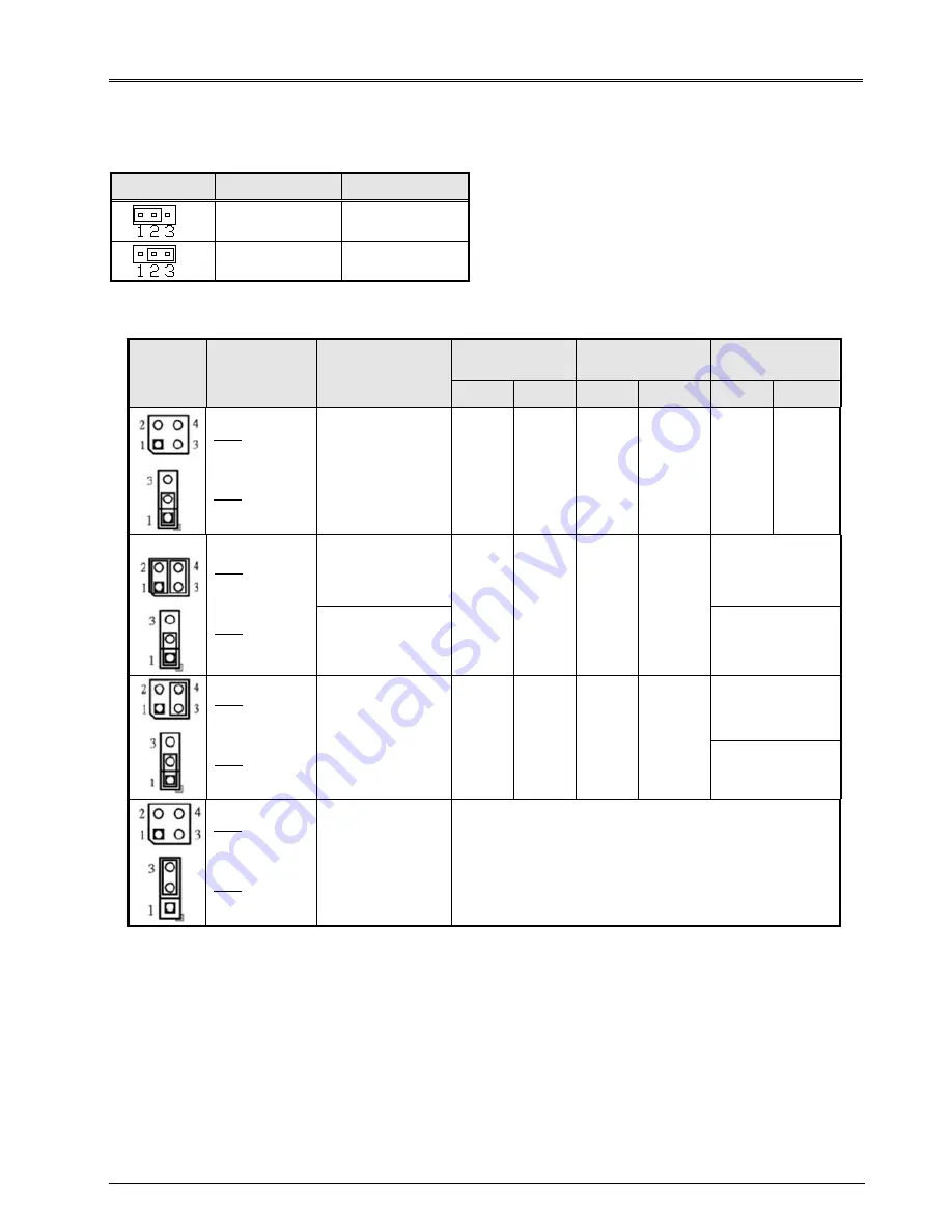
The Jumpers
JP1: Clear CMOS Contents
Use JP1 to clear the CMOS contents.
Note that the power connector or jack should be disconnected from the board before clearing CMOS.
JP1
Setting
Function
Pin 1-2
Short/Closed
Normal
Pin 2-3
Short/Closed
Clear CMOS
JP4, JP5: LAN Bypass & WDT Reboot Setting
JP4
JP5
Setting
Function
Power
OFF
Power
ON
Power ON
OS run software
Normal Bypass Normal Bypass Normal Bypass
JP4
1-2 & 3-4
Open
JP5
1-2 Closed
LAN bypass
upon the time
out of WDT.
JP4
1-2 & 3-4
Closed
JP5
1-2 Closed
System will
reboot upon the
time out of WDT.
LAN Always
Bypass
System will
reboot upon the
time out of WDT.
WDT Reboot
System
JP4
3-4 Closed
1-2 Open
JP5
1-2 Closed
LAN bypass &
system reboot
upon the time
out of WDT.
LAN Always
Normal
WDT Reboot
System
JP4
1-2 & 3-4
Open
JP5
2-3 Closed
LAN bypass
controlled by
Super IO GP54
or setting in
BIOS.
BIOS Setting **
GP54 Active:
Low: Bypass
High: Normal
** Note that the Bypass setting in BIOS is only working when JP4 & JP5 are set as this configuration.
D
efa
ult
S
ett
in
g


