background image

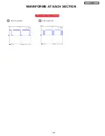
WAVEFORMS AT EACH SECTION

TABLE OF CONTENTS

I

001 

Pin 

4

 Main Sync                                    

I

401

 Pin 

5

4

 Main P

R

 OUT                           I401 Pin 55 Main P

B

 OUT

I401 Pin 56 Main Y OUT

                              I

700


Pin

 12 

R

in1


I

700

 Pin 1

0

 G

in1

I

700

 Pin 

7

 B

in1

1

2

3

4

5

6

7

8

                                                                      9

I

700

 Pin 

24


VD OUT          

                               I

700

 Pin 

25

 H

D

 OUT

11


P7A0/F0/K0

 Pin 

DY

10

   I

700

 Pin 3

1


CLK OUT

1

2   

  P7A0/F0/K0 Pin 5 LCCOM

Click  on  number  to  go  to  schematic

120

LC5

7

Summary of Contents for LC57

Page 1: ... instructions are for use by qualified service personnel only To reduce the risk of electric shock do not perform any servicing other than that contained in the operating instructions unless you are qualified to do so Before servicing this chassis it is important that the service technician read the IMPORTANT SAFETY INSTRUCTIONS in this service manual SAFETY NOTICE USE ISOLATION TRANSFORMER WHEN S...

Page 2: ...as become defective or inadvertently defeated during servicing Therefore the following checks should be performed for the con tinued protection of the customer and service technician Leakage Current Cold Check With the AC plug removed from the 120V AC 60Hz source place a jumper across the two plug prongs Using an insulation tester DC500V connect one lead to the jumpered AC plug and touch the other...

Page 3: ...ns it is not meant for the casual do it yourselfer Qualified technicians have the necessary test equipment and tools and have been trained to properly and safely repair complex prod ucts such as those covered by this manual Improperly per formed repairs can adversely affect the safety and reliability of the product and may void warranty Consumers should not risk trying to do the necessary repairs ...

Page 4: ...tically Sensitive ES Devices Some semiconductor solid state devices can be damaged easily by static electricity Such components commonly are called Electrostatically Sensitive ES Devices Examples of typical ES devices are integrated circuits and some field effect transistors and semiconductor chip components The following techniques should be used to help reduce the incidence of component damage c...

Page 5: ... the standard technique as outlined in paragraphs 5 and 6 above Removal 1 Desolder and straighten each IC lead in one operation by gent ly prying up on the lead with the soldering iron tip as the solder melts 2 Draw away the melted solder with an anti static suction type sol der removal device or with solder braid before removing the IC Replacement 1 Carefully insert the replacement IC in the circ...

Page 6: ...round the IC pin Solder the IC connection 4 Route the jumper wire along the path of the cut away copper pattern and let it overlap the previously scraped end of the good copper pattern Solder the overlapped area and clip off any excess jumper wire At Other Connections Use the following technique to repair defective copper pattern at connections other than IC Pins This technique involves the instal...

Page 7: ...with a miniature alligator clip and apply heat to the pad area with a 30 watt iron until solder flows Do not apply heat for more than 3 seconds How to Replace Flat lC Required Tools Soldering iron iron wire or small awl De solder braids Magnifier 1 Remove the solder from all of the pins of a Flat lC by using a de solder braid 2 Put the iron wire under the pins of the Flat lC and pull it in the dir...

Page 8: ...emove previous solder as much as possible from the soldering point When soldering please perfectly melt the lead free solder to mix well with the previous solder 3 Soldering iron for lead free solder Melting point of lead free solder is higher than solder containing lead Use of a soldering tool with temperature control and with much thermal capacitance is recommended Recommended temperature contro...

Page 9: ...ions However there is no guarantee that interference will not occur in a particular installation If this equipment does cause harmful interference to radio or television reception which can be determined by turning the equipment off and on the user is encouraged to try to correct the interference by one or more of the following measures Reorient or relocate the receiving antenna Increase the separ...

Page 10: ...orporated under license from SRS Labs Inc Technology Manufactured under license from Dolby Laboratories Dolby and the double D symbol are trademarks of Dolby Laboratories Technology HDMI the HDMI logo and High Definition Multimedia Interface are trademarks or registered trademarks of HDMI Licensing LLC INPUTS Power Input AC 120V 60Hz Stand by Power Less than 1 Watt Power Consumption Refer to rear ...

Page 11: ...T In Optical Out MM Card 1 50V720 2 2 2 1 1 1 1 1 2 1 1 2 3 4 5 6 7 8 9 10 REAR FRONT or SIDE No MODEL NAME POD Card IEEE 1394 A V In S video In Photo USB 1 50V720 1 1 1 1 2 3 4 5 6 7 8 9 10 Remark 1 Monitor out and Audio to HiFi share one terminal and switched by user menu See I B Terminals and other function about the electrical specifications ...

Page 12: ...FT Active matrix 3 Pixels 1284 H x 724 V 4 Panel size 0 7 5 Dot pitch 12 µm 6 Life time More than 20 000h Ta 25 C worst UV filter combination LCD panel is UV light sensitive device UV ray which illuminates LCD panel should be cut with three UV filters with 50 cut wavelength of 430nm 430nm 430nm nominal and 427nm 427nm 426nm worst combination 2 Lamp No Item Description 1 Input electricity 120W 2 Ma...

Page 13: ... screen If so drapes or screens can be used to reduce the reflection or the TV can be located in a different section of the room If the TV s audio output will be connected to a Hi Fi system s external speakers the best audio performance will be obtained by placing the speakers equidistant from each side of the receiver cabinet and as close as possible to the height of the picture screen center For...

Page 14: ...orders VCRs and laser disc players with an S Video feature in place of the standard video cable to produce a high quality picture Optical Cable This cable is used to connect to an audio amplifier with an Optical Audio In jack Use this cable for the best sound quality HDMI Cable This cable is used to connect your external devices such as Set Top Boxes or DVD players equipped with an HDMI output con...

Page 15: ...mode settings between DAY and NIGHT mode PIP BUTTON TV Press to show and change the Picture in Picture mode EXIT BUTTON TV CBL SAT Exits out of the OSD or INPUTS menu systems if their menu is displayed FAVORITE CHANNEL FAV CH button TV Press to enter access Favorite Channel FAV mode GUIDE BUTTON SAT STB CBL Accesses the program guide of other devices INFO BUTTON TV CBL SAT Displays various informa...

Page 16: ...ns for your desired sound level The volume level will be displayed on the TV screen These buttons also serve as the cursor left and right buttons when in MENU mode When the TV power is turned OFF at a volume level 31 or greater the volume level will default to 30 when the TV is turned ON However if it is set to a level 30 or less the volume level will be at the level it was set when the TV is turn...

Page 17: ...OKEN LAMP WRONG LAMP UNIT ASSEMBLY LAMP DOOR OPEN Too hot inside the OPTIC unit COOLING FAN STOPPED BEGINNING OF WARM UP AFTER THE POWER ON NORMAL OPERATION BEGINNING OF COOL DOWN FOR 20 SEC TV CANNOT ACCEPT ANY CODE IN THIS PERIOD EXCEPT WITHIN THE BEGINNING 5 SEC COOL DOWN FOR 6 MINUTES TV CAN ACCEPT REMOTE CONTROL AND SIDE BUTTONS LIGHT ON BLINKING LIGHT ON BLINKING INTERMEDIATE BLINKING 0 5 SE...

Page 18: ... examples NOTE 1 Completely insert connection cord plugs when connecting to side panel jacks If you do not the played back picture may be abnormal 2 If you have a S VHS VCR use the S INPUT cable in place of the standard video cable 3 If you have a mono VCR insert the audio cable into the left audio jack of your TV S VIDEO VIDEO AUDIO L MONO R INPUT 5 S VIDEO VIDEO AUDIO L MONO R INPUT 5 ...

Page 19: ...nfringement the MONITOR OUT output will be abnormal when using the Y PBPR jacks 6 INPUT 3 and INPUT 4 Y VIDEO can be used for composite video and component video input HDMI High Definition Multimedia Interface ABOUT HDMI HDMI is the next generation all digital interface for consumer electronics HDMI enables the secure distribution of uncompressed high definition video and multi channel audio in a ...

Page 20: ... CableCARD is installed wait until the second screen below appears The third screen below will appear if a channel is not authorized for viewing Press the EXIT button to exit the second screen Please take note of all information on the screen you will provide this information to your cable operator Call your cable operator and give them the information from the card to start your cable service Not...

Page 21: ...leCARD Information After the CableCARD has been successfully installed a CableCARD Information menu appears in the SETUP menu of the On Screen Display Follow the instructions below to access the CableCARD Information menu Set The Inputs Lamp Power Control Set Closed Captions Menu Preference Set Monitor Out CableCARD Information Setup Upgrades Quick Start Up Move SEL Select Setup Timers Locks Chann...

Page 22: ...input You may use composite and component video signals for INPUT 3 and INPUT 4 It may be necessary to adjust TINT to obtain optimum picture quality when using the Y PBPR inputs To ensure no copyright infringement the MONITOR OUT output may be abnormal when using the Y PBPR jacks When using an HDMI input from a Set Top Box it is recommended that a 1080i or 720p input signal is used NOTE 1 Connect ...

Page 23: ...a fixed digital audio output to your external component such as an A V receiver with optical input capability The audio level can only be controlled through the volume control of the external audio amplifier R L A U D I O V I D E O S I V I D E O MONO MONO MONO MONO PR PB Y VIDEO Y VIDEO PR PB PR PB PR PB MONITOR OUT AUDIO TO HI FI INPUT 1 CABLE AIR INPUT 2 TV AS CENTER INPUT 3 INPUT 4 CableCARD CA...

Page 24: ...ecycling and disposal information go to www lamprecycle org For product recycling and disposal information contact your local government agency or eRecycle org in California the Electronic Industries Alliance at www eiae org in the US or the Electronic Product Stewardship Canada at www epsc ca in Canada For more information call 1 800 HITACHI CAUTION A LAMP indicator will light when lamp becomes h...

Page 25: ...until the quick snap on disengages NOTE This product contains lead and a lamp that contains mercury Dispose of this product and its lamp in accordance with applicable environmental laws For lamp recycling and disposal information go to www lamprecycle org For product recycling and disposal information contact your local government agency or the Electronic Industries Alliance at www eiae org in the...

Page 26: ...your fingers NOTE Do not put your hand in the Lamp Storage area after the Lamp Unit is removed your may get burned 5 Replace with the new lamp Place the removed lamp into the empty box of the replacement lamp Do not touch the front glass of the new lamp or its receptacle This may shorten the life of the lamp and reduce the picture quality Push the lamp unit back to its original position Tighten th...

Page 27: ...he front cover until you hear a snap Push the other snap on gently to make a good fit 8 Plug power cord into AC outlet and turn on the main power switch NOTE This product contains lead and a lamp that contains mercury Dispose of this product and its lamp in accordance with applicable environmental laws For lamp recycling and disposal information go to www lamprecycle org For product recycling and ...

Page 28: ... five video inputs have independent Aspect Style settings 2 Vertical position adjustments are directly available when you choose 4 3 EXPANDED ZOOM1 ZOOM2 or 16 9 ZOOM aspect style 4 3 STANDARD Use this aspect mode to display conventional 4 3 images Side panels gray areas are placed to the left and right of the image to preserve the original aspect ratio of the source Note Use this mode for only 15...

Page 29: ...b Aspect 16 9 4 3 16 9 16 9 4 3 POP ANT Digital 16 9 Yes Yes Yes 480p 480i 16 9 Yes1 Yes1 ANT Analog 4 3 Yes Yes S Video Video PIP ANT Digital 16 9 Yes1 Yes 4 3 1080i 720p 16 9 Yes 480p 480i 16 9 Yes2 S Video Video PIP ANT Digital 16 9 Yes Yes2 16 9 1080i 720p 16 9 Yes 480p 480i 16 9 Yes2 S Video Video SPLIT ANT Digital 16 9 Yes Yes Yes 4 3 Yes Yes Yes 1080i 720p 16 9 Yes Yes 480p 480i 16 9 Yes Ye...

Page 30: ...to freeze three frames of the picture you are currently viewing only the 3 sub pictures will freeze Press the EXIT button to return to normal viewing This feature is useful for viewing a moving picture that has many details for example a close play in a sporting event or a golf swing NOTE 1 The default FREEZE mode is the MAIN freeze followed by the SPLIT freeze and then the STROBE freeze The last ...

Page 31: ...r Protection Operation Check 39 2 13 High Temperature Protection Operation Check 39 2 14 Temperature Sensor Data Setting 40 2 15 Checking of Temperature Sensor 41 2 16 Adjustment I2 C Parameter List 42 2 17 Adjustment OSD Flow Chart 79 2 18 Troubleshooting Flow Charts 88 IMPORTANT For many of the above adjustments it is necessary to have an HDTV 1080i or 720P signal generator SDTV 480P signal gene...

Page 32: ...n use the NUMBER pad on the R C example select SEINE press 69 then SELECT the DATA shown is EB if this DATA needs to be change press the keys to modify when finish press SELECT key to store the new DATA value normal condition C After finishing the necessary adjustment press the R C EXIT key or EXIT key on the side panel Adjustment mode is released and LCD set returns to normal condition 1 2 MEMORY...

Page 33: ... NOTE The execution of this function returns the adjustment made by the customer this will return all the adjustments to the original shipping conditions Procedure 1 Enter Adjustment mode by the method described in sub items 1 1 and 1 2 from item 1 Adjustment procedure start up 2 Get to the second page of Adjust Mode by pressing remote control Menu key once or with either the R C or front panel cu...

Page 34: ...int OFFSET value Adjustment range 2 5 GHOST ADJUSTMENT ADJUSTMENT PROCEDURE 1 ADJ SIGNAL Internal signal from IC Black window pattern with RGB raster signal ADJUSTMENT 2 RED GHOST LCD ADJUST MODE ĺ GHOST LCD ADJUST MODE GHOST R xx GHOST G xx GHOST B xx Press SELECT key test pattern will be displayed 3 Increase the I2 C data by pressing cursor stick Ź of handset until ghost appears at left side of ...

Page 35: ... 50 0 5 1 0 16mm 60 0 5 1 0 20mm H size marker 42 0 5 1 0 14mm 50 0 5 1 0 16mm 60 0 5 1 0 20mm 42 7mm 50 8mm 60 10mm 70 12mm Normal mode Outer edge of the circle Inner edge of the circle 5 3 3 5 Top and bottom of the circle is between outer edge and inner edge BACK TO ADJUSTMENTS 35 LC57 ...

Page 36: ...minance level is divided into 32 No 0_No 32 FOR EXAMPLE If customer require to change the white balance of 12th level of white to reddish increase the red value and adjust the white balance of 12th signal level see below I2C MENU LCDADJ GAMMA No 12 Adjustment STORE THE DATA TO TV SET LCD ADJ G C WRITE_press for several second After this procedure this new data will be write back to E2PROM It takes...

Page 37: ...UNIFORMITY ADJUSTMENT PROCEDURE Adjustable luminance level is divided in 4 MIN 8 MIDL 20 MIDH 55 and HMAX 82 FOR EXAMPLE If a customer complains about the color uniformity at position 5 on the screen luminance level MIDH increase the BLUE or GREEN or RED value and adjust the color uniformity of position 5 I 2 C MENU LCD ADJ C UNIF MIDH POINT No 5 STORE THE DATA TO TV SET LCD ADJ G C WRITE press fo...

Page 38: ... GHOST B xxx Press SELECT key test pattern will be displayed Check that no ghost on right hand side of the window If there is decrease Ghost by pressing cursor stick ŻŹ of handset Press SELECT key of handset return to the LCD ADJUST MODE 3 Sub Ghost G adjustment Press ٕ key to select green Check and adjust sub ghost green with same procedure as Red SUB GHOST 4 Sub Ghost B adjustment Press ٕ key to...

Page 39: ...or flash red 3 Turn the set off and attach Lamp holder again 2 13 HIGH TEMPERATURE PROTECTION OPERATION CHECK Adjustment procedure 1 Remove EPF2 connector while the set is on 2 Check that the lamp is turned off and Temp indicator flash red 3 Turn the set off and attach EPF2 again 4 Remove EPF3 connector while the set is on 5 Check that the lamp is turned off and Temp indicator flash red 6 Turn the...

Page 40: ...nd message OSD cannot be displayed ii IL01 failed or not connected TEMP LED and LAMP LED are blinking alternately Cycle 1sec 2 14 2 Purpose It s important to set the limiting data correctly And it s better to use the automatic adjustment then human mistake is prevented Because each model needs the unique data that is different from another models 2 14 3 Adjustment Spec Adjustment procedure 1 Open ...

Page 41: ... message OSD will be displayed in a minute Simplified method Check that front LEDs are not blinking alternately after power ON Device error blinking 2 15 1 Timing of the sensor operation as Appendix 3 minutes Device Error cannot be checked 1 minute Average the data Start displaying OSD Power Device Error is checked once Starting of monitoring Starting of displaying data 71 Starting of checking the...

Page 42: ...PROM for Drive Micro Initial Data HEX Adjustment Mode OSD Adjustment Item Adjustment Range HEX LC58E LC58 LC57 Drive Up E7070 STRIPE_G0 LCD Adjust STRIPE0 G E7070 C4Bh 00 FF 008 ĸ ĸ ĸ STRIPE_G1 LCD Adjust STRIPE1 G E7070 C4Ch 00 FF 002 ĸ ĸ ĸ STRIPE_G2 LCD Adjust STRIPE2 G E7070 C4Dh 00 FF 000 ĸ ĸ ĸ STRIPE_G3 LCD Adjust STRIPE3 G E7070 C4Eh 00 FF 0FB ĸ ĸ ĸ STRIPE_G4 LCD Adjust STRIPE4 G E7070 C4Fh ...

Page 43: ...D Adjust G UNIF MIN 00 FF 1 ĸ ĸ ĸ B LCD Adjust B UNIF MIN 00 FF 1 ĸ ĸ ĸ No 1 25 LCD Adjust C UNIF NO 01 19 01 ĸ ĸ ĸ R LCD Adjust R UNIF MIN 00 FF 1 ĸ ĸ ĸ G LCD Adjust G UNIF MIN 00 FF 1 ĸ ĸ ĸ B LCD Adjust B UNIF MIN 00 FF 1 ĸ ĸ ĸ No 1 25 LCD Adjust C UNIF NO 01 19 01 ĸ ĸ ĸ R LCD Adjust R UNIF MIN 00 FF 1 ĸ ĸ ĸ G LCD Adjust G UNIF MIN 00 FF 1 ĸ ĸ ĸ B LCD Adjust B UNIF MIN 00 FF 1 ĸ ĸ ĸ G C_WRITE 2n...

Page 44: ...0 ĸ ĸ ĸ ID1_SLiCE_LEVEL ISLICEL ID1 Slice Level 00 03 00 ĸ ĸ ĸ ID1_AMP IRWIDON ID1 Amplitude Detect 00 01 01 ĸ ĸ ĸ ID1_PHASE_SEL IEDGES ID1 Phase Select 00 01 00 ĸ ĸ ĸ ID1_PHASE_WiDTH IRTIMS ID1 Detection Phase Width 00 01 00 ĸ ĸ ĸ 3rd page 2 2 Initial Data HEX Adjustment Mode OSD Adjustment Item Adjustment Range HEX LC58E LC58 LC57 TC90103 G_READ_OUT GGSON Guide Slice Read Output 00 01 01 ĸ ĸ ĸ G...

Page 45: ...12 ISF Mode LCD DRIVE B SUB GAIN B W Color Temperature B W 000 3FF 148 ĸ ĸ ĸ 013 LCD DRIVE VREF 00 FF ĸ ĸ ĸ 014 LCD DRIVE SHPR 00 0F 07 ĸ ĸ ĸ 015 LCD DRIVE SHRG 00 0F 07 ĸ ĸ ĸ 016 LCD DRIVE SHRB 00 0F 07 ĸ ĸ ĸ Drive Micro 2 2 Initial Data HEX Adjustment Mode OSD Adjustment Item Adjustment Range HEX LC58E LC58 LC57 Drive Micro E7070 017 LCD DRIVE NRSH LR 000 3FF 1F0 φ φ φ 018 LCD DRIVE NRSH LG 000 ...

Page 46: ...SD Adjustment Item Adjustment Range HEX LC58E LC58 LC57 SEINE 036 Color Signal Round Coefficient for Noise Reduction NTSC 480i Input only 00 0D 0A φ φ φ 037 Color Signal Frame Difference Limit for Noise Reduction NTSC 480i Input only 00 1F 03 φ φ φ 038 Enhance Movement Mode 00h Enhancer 2nd V filter OFF 01h Enhancer ON 02h 2nd V filter ON 03h Reserved 00 03 00 φ φ φ 039 Enhancer Movement Mode Sele...

Page 47: ...ure Sensor 1 Read Data 00 FF φ φ φ 075 Reserve Alarm 1 Start Temperature Setting 00 FF 4B φ φ φ 076 Reserve Alarm 1 Stop Temperature Setting 00 FF 41 φ φ φ FC6 1 20 Initial Data HEX Adjustment Mode OSD Adjustment Item Adjustment Range HEX LC58E LC58 LC57 FC6 001 ISF Mode Black Stretch 00h OFF 01h DBS 02h HBS 00 02 01 φ φ φ 002 ISF Mode Black Correction 00h OFF 01h DBS 02h HBS 00 02 01 φ φ φ 003 IS...

Page 48: ...0 φ φ φ 033 ISF Mode Blue Line 4 Setting 000 3FF 100 φ φ φ 034 ISF Mode Blue Line 5 Setting 000 3FF 140 φ φ φ 035 ISF Mode Blue Line 6 Setting 000 3FF 180 φ φ φ FC6 3 20 Initial Data HEX Adjustment Mode OSD Adjustment Item Adjustment Range HEX LC58E LC58 LC57 FC6 036 ISF Mode Blue Line 8 Setting 000 3FF 200 φ φ φ 037 ISF Mode Blue Line 10 Setting 000 3FF 280 φ φ φ 038 ISF Mode Blue Line 12 Setting...

Page 49: ...9 ISF Mode Y Vertical Enhancer OFF 00 01 00 φ φ φ FC6 5 20 Initial Data HEX Adjustment Mode OSD Adjustment Item Adjustment Range HEX LC58E LC58 LC57 FC6 080 ANT NTSC DAY 00 1F 0A φ φ φ 081 480i DAY 00 1F 0A φ φ φ 082 480p DAY 00 1F 0A φ φ φ 083 1080i 720p DAY 00 1F 0A φ φ φ 084 ISF Mode Y Vertical Enhancer Gain Adjustment ALL NIGHT 00 1F 0A φ φ φ 085 ANT 00 03 00 φ φ φ 086 NTSC 00 03 00 φ φ φ 087 ...

Page 50: ...1080i 720p 00 01 00 φ φ φ 123 ANT 00 1F 3F φ φ φ 124 NTSC 00 1F 3F φ φ φ 125 480i 00 1F 3F φ φ φ 126 480p 00 1F 3F φ φ φ 127 ISF Mode Y Horizontal Clip Offset Level 1080i 720p 00 1F 3F φ φ φ FC6 7 20 Initial Data HEX Adjustment Mode OSD Adjustment Item Adjustment Range HEX LC58E LC58 LC57 FC6 128 ANT NTSC 480i 00 FF 00 φ φ φ 129 ISF Mode Y Horizontal Non Linear Peaking 480p 1080i 720p 00 FF 00 φ φ...

Page 51: ...φ 170 Histogram Gamma APL Point 0 Gamma Select High 00 02 01 φ φ φ FC6 9 20 Initial Data HEX Adjustment Mode OSD Adjustment Item Adjustment Range HEX LC58E LC58 LC57 FC6 171 Histogram Gamma APL Point 1 Gamma Select High 00 02 00 φ φ φ 172 Histogram Gamma APL Point 2 Gamma Select High 00 02 01 φ φ φ 173 Histogram Gamma APL Point 3 Gamma Select High 00 02 02 φ φ φ 174 Histogram Gamma APL Point 4 Gam...

Page 52: ...icture 000 3FF 8A φ φ φ 215 Gamma Line 9 Setting for Very Bright Picture 000 3FF 7C φ φ φ FC6 11 20 Initial Data HEX Adjustment Mode OSD Adjustment Item Adjustment Range HEX LC58E LC58 LC57 FC6 216 for Dark Picture 000 3FF 8E φ φ φ 217 for Standard 000 3FF 86 φ φ φ 218 for Bright Picture 000 3FF 76 φ φ φ 219 Gamma Line 8 Setting for Very Bright Picture 000 3FF 6C φ φ φ 220 for Dark Picture 000 3FF...

Page 53: ... LC58 LC57 FC6 263 Black Stretch Black Correction Speed 00h Fast 10h Slow 00 10 00 φ φ φ 264 Black Stretch Black Correction Reset ǻAPL 00 FF 0A φ φ φ 265 Black Stretch Black Correction Reset APL 00 FF 32 φ φ φ 266 Black Stretch Black Correction Speed Up ǻAPL 00 FF 0E φ φ φ 267 Black Stretch Black Correction Speed Up Step 00h Direct 01h Slow FFh Fast 00 FF 00 φ φ φ 268 Black Stretch Gain Up Step 0 ...

Page 54: ...t Correction Offset 00 FF 00 φ φ φ 305 Black Correction Contrast Correction Value 00 FF φ φ φ FC6 15 20 Initial Data HEX Adjustment Mode OSD Adjustment Item Adjustment Range HEX LC58E LC58 LC57 FC6 306 Back Light Correction Speed 00h Fast 3Fh Slow 00 10 05 φ φ φ 307 Back Light Correction Up Step 00h Direct 01h FFh Adjustment㬍4 256step 00 FF 40 φ φ φ 308 Back Light Correction Down Step 00h Direct 0...

Page 55: ...nitial Data HEX Adjustment Mode OSD Adjustment Item Adjustment Range HEX LC58E LC58 LC57 FC6 345 Shading OFFψ10 00 FF 33 φ φ φ 346 Shading 10 ψOFF 00 FF 1F φ φ φ 347 Shading 10 ψ20 00 FF 3A φ φ φ 348 Shading 20 ψ10 00 FF 26 φ φ φ 349 Shading 20 ψ30 00 FF 41 φ φ φ 350 Shading 30 ψ20 00 FF 2D φ φ φ 351 Histogram Detection Average Value 00 10 05 φ φ φ 352 Histogram Area Start Position 00 07 04 φ φ φ ...

Page 56: ...htness Level Detection 00 FF φ φ φ 394 Average Brightness Level Detection 00 FF φ φ φ 395 Brightness Histogram Detection 0 0000 FFFF φ φ φ 396 Brightness Histogram Detection 1 0000 FFFF φ φ φ 397 Brightness Histogram Detection 2 0000 FFFF φ φ φ 398 Brightness Histogram Detection 3 0000 FFFF φ φ φ 399 Brightness Histogram Detection 4 0000 FFFF φ φ φ 400 Brightness Histogram Detection 5 0000 FFFF φ ...

Page 57: ...nt Mode OSD Adjustment Item Adjustment Range HEX LC58E LC58 LC57 FC4 001 ISF Mode Dynamic Enhancer 00h APL Motion Adjustment Enhancer OFF 01h APL Synchronize Enhancer OFF 02h Motion Adjustment Enhancer 03h Active 00 03 03 φ φ φ 002 ISF Mode Dynamic Contrast Correction 00h OFF 01h Active 00 01 01 φ φ φ 003 Normal 00 FF 80 φ φ φ 004 HDMI DVI Setup Cancel OFF 00 FF 80 φ φ φ 005 ISF Mode Contrast Cent...

Page 58: ...φ φ 032 720p 00 0F 00 φ φ φ 033 ISF Mode Horizontal Enhance Coring Reserve 00 0F 00 φ φ φ FC4 3 19 Initial Data HEX Adjustment Mode OSD Adjustment Item Adjustment Range HEX LC58E LC58 LC57 FC4 034 ANT_Mode1 00 03 02 φ φ φ 035 ANT_Mode2 5 00 03 02 φ φ φ 036 NTSC 00 03 02 φ φ φ 037 480i 00 03 02 φ φ φ 038 480p 00 03 02 φ φ φ 039 1080i 720p 00 03 01 φ φ φ 040 ALL NIGHT 00 03 00 φ φ φ 041 Reserve 00 0...

Page 59: ...0h CLIP ON 01h CLIP OFF 1080i 720p 00 01 00 φ φ φ FC4 5 19 Initial Data HEX Adjustment Mode OSD Adjustment Item Adjustment Range HEX LC58E LC58 LC57 FC4 074 ANT 00 0F 0B φ φ φ 075 NTSC 00 0F 0B φ φ φ 076 480i 00 0F 0B φ φ φ 077 480p 00 0F 0A φ φ φ 078 1080i 720p 00 0F 0A φ φ φ 079 ISF Mode Y Horizontal Enhancer Gain ALL NIGHT 00 0F 0A φ φ φ 080 ANT 00 0F 07 φ φ φ 081 NTSC 00 0F 07 φ φ φ 082 480i 0...

Page 60: ...0i 00 3F 00 φ φ φ 117 ISF Mode Y Vertical Nonlinear Peaking 480p 1080i 720p 00 3F 00 φ φ φ FC4 7 19 Initial Data HEX Adjustment Mode OSD Adjustment Item Adjustment Range HEX LC58E LC58 LC57 FC4 118 ANT_Mode1 00 07 03 φ φ φ 119 ANT Mode2 00 07 03 φ φ φ 120 ANT Mode3 00 07 03 φ φ φ 121 ANT Mode4 00 07 03 φ φ φ 122 ANT Mode5 00 07 03 φ φ φ 123 NTSC Composite 00 07 04 φ φ φ 124 NTSC Y C 00 07 04 φ φ φ...

Page 61: ... φ φ 161 480i 00 1F 0D φ φ φ 162 APL Enhancer Correction Value 1080i 00 1F 0C φ φ φ 163 Horizontal Vertical Enhancer Setting Value 00 1F φ φ φ 164 Moving Enhancer Speed 00 10 0A φ φ φ FC4 9 19 Initial Data HEX Adjustment Mode OSD Adjustment Item Adjustment Range HEX LC58E LC58 LC57 FC4 165 ANT NTSC 480i 00 FF 12 φ φ φ 166 Moving Enhancer Start Frame Differential 480p 1080i 720p 00 FF 0A φ φ φ 167 ...

Page 62: ... φ φ 203 480p 00 07 00 φ φ φ 204 Main Sub YNR Passage Level Limit 1080i 720p 00 07 00 φ φ φ FC4 11 19 Initial Data HEX Adjustment Mode OSD Adjustment Item Adjustment Range HEX LC58E LC58 LC57 FC4 205 ANT 00 07 04 φ φ φ 206 NTSC 00 07 04 φ φ φ 207 480i 00 07 04 φ φ φ 208 480p 00 07 04 φ φ φ 209 Main Sub YNR Input Level Gain 1080i 720p 00 07 04 φ φ φ 210 Main YNR Reducing Gain 00 07 02 φ φ φ 211 Sub...

Page 63: ...D Yellow 000 3FF 3FF φ φ φ 245 C M OFF Phase2 Hue Slope CCD Yellow 00h 128 80h 0 FFh 127 00 FF 80 φ φ φ FC4 13 19 Initial Data HEX Adjustment Mode OSD Adjustment Item Adjustment Range HEX LC58E LC58 LC57 FC4 246 C M OFF Phase3 Hue Center CCD Green Green Data Tint 360 1024 225 360 1024 640 280h 000 3FF 280 φ φ φ 247 C M OFF Phase3 Hue Width CCD Green 000 3FF 100 φ φ φ 248 C M OFF Phase3 Hue Clip CC...

Page 64: ...HEX Adjustment Mode OSD Adjustment Item Adjustment Range HEX LC58E LC58 LC57 FC4 278 C M OFF Gain3 Hue Center CCD Green Green Data Tint 360 1024 225 360 1024 640 280h 000 3FF 280 φ φ φ 279 C M OFF Gain3 Hue Width CCD Green 000 3FF 100 φ φ φ 280 C M OFF Gain3 Hue Clip CCD Green 000 3FF 3FF φ φ φ 281 C M OFF Gain3 Hue Slope CCD Green 00h 128 80h 0 FFh 127 00 FF 80 φ φ φ 282 C M OFF Gain4 Hue Center ...

Page 65: ...n 000 3FF 3FF φ φ φ 313 C M OFF Phase3 Hue Slope Paper Green 00h 128 80h 0 FFh 127 00 FF 80 φ φ φ FC4 17 19 Initial Data HEX Adjustment Mode OSD Adjustment Item Adjustment Range HEX LC58E LC58 LC57 FC4 314 C M OFF Phase4 Hue Center Paper Cyan Cyan Data Tint 360 1024 293 2 360 1024 834 342h 000 3FF 342 φ φ φ 315 C M OFF Phase4 Hue Width Paper Cyan 000 3FF 100 φ φ φ 316 C M OFF Phase4 Hue Clip Paper...

Page 66: ...ue 00h 128 80h 0 FFh 127 00 FF 80 φ φ φ FC4 19 19 Initial Data HEX Adjustment Mode OSD Adjustment Item Adjustment Range HEX LC58E LC58 LC57 FC4 346 C M OFF Gain6 Hue Center Paper Other_1 Data Tint 360 1024 000 3FF 000 φ φ φ 347 C M OFF Gain6 Hue Width Paper Other_1 000 3FF 100 φ φ φ 348 C M OFF Gain6 Hue Clip Paper Other_1 00 3FF 3FF φ φ φ 349 C M OFF Gain6 Hue Slope Paper Other_1 00h 128 80h 0 FF...

Page 67: ...00 φ φ φ TC90103 2 12 Initial Data HEX Adjustment Mode OSD Adjustment Item Adjustment Range HEX LC58E LC58 LC57 TC90103 ANT NTSC 480i 016 ANT NTSC 00 03 01 φ φ φ 017 Sharpness Noise Cancel Coring 00h䋺0 8 IRE 01h䋺1 6 IRE 02h䋺3 2 IER 03h䋺6 4 IRE Y C 480i 00 03 01 φ φ φ 018 Noise Cancel Gain 00h䋺OFF 01h䋺㬍1 4 0h2䋺 1 2 03h䋺 1 00 03 00 φ φ φ 019 LTI Gain LTI Luminance Transient Improvement 00h䋺OFF 01h䋺 ...

Page 68: ...01 01 φ φ φ 056 Vertical Y Noise Cancel Limiter 00h䋺8lsb 01h䋺16lsb 00 01 00 φ φ φ 057 Vertical Y Noise Cancel Gain 00h䋺㬍1 01h䋺㬍2 00 01 00 φ φ φ TC90103 4 12 Initial Data HEX Adjustment Mode OSD Adjustment Item Adjustment Range HEX LC58E LC58 LC57 TC90103 ANT NTSC 480i 058 Vertical Y ON 00h䋺OFF 01h䋺ON 00 01 01 φ φ φ 059 C NY Limiter 00h䋺16lsb 01h䋺24lsb 00 01 00 φ φ φ 060 C NC Gain 00 01 00 φ φ φ 06...

Page 69: ...h䋺8 01h䋺16 02h䋺24 03h䋺32 00 03 01 φ φ φ 094 1 Field Y Detection Slope Color Still Picture Edge 00h䋺1 2 03h䋺㺙 02 00 03 01 φ φ φ 095 1 Field Y Detection Offset Color Still Picture Edge 00h䋺Still Picture 0Fh䋺Motion Picture 0C Center 00 0F 00 φ φ φ TC90103 6 12 Initial Data HEX Adjustment Mode OSD Adjustment Item Adjustment Range HEX LC58E LC58 LC57 TC90103 ANT NTSC 480i 096 Y Motion Picture Distincti...

Page 70: ...icture 0Ch Center 00 0F 08 φ φ φ 125 2 Field Detection 2nd Slope Threshold Y Still Picture Smooth 00h䋺0 01h䋺1 02h䋺2 03h䋺3 00 03 00 φ φ φ TC90103 8 12 Initial Data HEX Adjustment Mode OSD Adjustment Item Adjustment Range HEX LC58E LC58 LC57 TC90103 ANT NTSC 480i 126 2 Field Detection Slope Y Motion Picture Edge 00h䋺1 2 03h䋺㺙 02h Default 00 03 03 φ φ φ 127 2 Field Detection Offset Y Motion Picture E...

Page 71: ...t 00 0F 08 φ φ φ 153 AGC Manual Setting AGC Auto Gain Control 00h䋺OFF 01h䋺ON 00 01 00 φ φ φ 154 AGC Manual Gain Setting AGC Auto Gain Control 00 7F 28 φ φ φ 155 AGC Sync Level Detection ON OFF AGC Auto Gain Control 00h䋺OFF 01h䋺ON 00 01 01 φ φ φ TC90103 10 12 Initial Data HEX Adjustment Mode OSD Adjustment Item Adjustment Range HEX LC58E LC58 LC57 TC90103 ANT NTSC 480i 156 AGC Peak Level Detection ...

Page 72: ... φ φ φ 187 Memory Write Vertical Start Phase Adjustment 08h䋺 8H 00h䋺0us 07h䋺 7H 00 0F 08 φ φ φ 188 Burst Gate Pulse Start Phase Adjustment 00h䋺0us 0Fh䋺 4 44us 02h Default 3 58MHz unit 00 0F 02 φ φ φ TC90103 12 12 Initial Data HEX Adjustment Mode OSD Adjustment Item Adjustment Range HEX LC58E LC58 LC57 TC90103 ANT NTSC 480i 189 Clamp Pulse Horizontal Adjustment for Ghost Canceller Tuner 08h䋺 1 185u...

Page 73: ...00 3FF φ φ φ 002 Vertical Number High Bit 000 7FF φ φ φ 003 480i 00 03 02 φ φ φ 004 480p 00 03 02 φ φ φ 005 1080i 00 03 02 φ φ φ 006 AFC loop gain control 00h H free running mode 01h gain low 02h gain middle 03h gain high 720p 00 03 02 φ φ φ 007 480i 00 07 07 φ φ φ 008 480p 00 07 07 φ φ φ 009 1080i 00 07 07 φ φ φ 010 Phase control Control for rough tune for HOUT 00h H sync center 01h center 3 125 ...

Page 74: ...I_1 2 001 VSYNC Clock detect Sync detect 1 00 07 φ φ φ 002 HDCP Status 00 FF φ φ φ 003 Pixel clock 00 FF φ φ φ 004 N hardware value 1 Low 7 bit 00 FF φ φ φ 005 N hardware value 1 Middle 7 bit 00 FF φ φ φ 006 N hardware value 1 High 4 bit 00 FF φ φ φ 007 CTS hardware value 1 Low 7 bit 00 FF φ φ φ 008 CTS hardware value 1 Middle 7 bit 00 FF φ φ φ 009 CTS hardware value 1 High 4 bit 00 FF φ φ φ 010 A...

Page 75: ...ON Vertical Position Adjustment 001 LCD DRIVE R SUB GAIN High 002 LCD DRIVE G SUB GAIN High 003 LCD DRIVE B SUB GAIN High 004 LCD DRIVE R SUB GAIN Medium 005 LCD DRIVE G SUB GAIN Medium 006 LCD DRIVE B SUB GAIN Medium 007 LCD DRIVE R SUB GAIN STD 008 LCD DRIVE G SUB GAIN STD 009 LCD DRIVE B SUB GAIN STD 010 LCD DRIVE R SUB GAIN B W 011 LCD DRIVE G SUB GAIN B W Drive Micro 012 LCD DRIVE B SUB GAIN ...

Page 76: ...cal Dynamic Shoot Balance Coring Adjustment 480p 1080i 720p 093 ANT NTSC 480i 094 480p FC6 095 Y Vertical Enhancer Clip OFF 1080i 720p ISF Adjustment Mode Device OSD Item 096 ANT 097 NTSC 098 480i 099 480p 100 1080i 720p 101 ANT NTSC 480i NIGHT 102 480p NIGHT 103 Y Vertical Clip Offset Level 1080i 720p NIGHT 104 ANT NTSC 480i 105 Y Vertical Non Linear Peaking 480p 1080i 720p 106 Y Horizontal Enhan...

Page 77: ...54 ANT Mode4 055 ANT Mode5 056 NTSC 057 480i 058 480p 059 1080i 060 720p 061 HDMI DVI 480i 062 HDMI DVI 480p VGA 063 HDMI DVI 1080i 064 HDMI DVI 720p 065 Reserve 066 Y Vertical and Horizontal Enhance Gain Reserve 067 ANT NTSC 068 480i 069 480p 070 Horizontal High Pass Filter Switch 1080i 720p 071 ANT NTSC 480i 072 480p 073 Y Horizontal Enhancer Clip Off 1080i 720p 074 ANT 075 NTSC 076 480i 077 480...

Page 78: ... 480i 117 Y Vertical Nonlinear Peaking 480p 1080i 720p 118 ANT_Mode1 119 ANT Mode2 120 ANT Mode3 121 ANT Mode4 122 ANT Mode5 123 NTSC Composite 124 NTSC Y C 125 480i 126 480p 127 1080i 128 720p 129 HDMI DVI 480i 130 HDMI DVI 480㨜 VGA 131 HDMI DVI 1080i 132 HDMI DVI 720p FC4 133 Y Coring Amplitude Reserve BACK TO ADJUSTMENTS 78 LC57 ...

Page 79: ...D ADJUST MODE RGB H POSITION ᇬV POSITION ENBW GHOST VCOM NRSH STRIPE S GHOST STREAK Ÿź CH U D INPUT LCD ADJUST MODE RGB H POSITION V POSITION ᇬENBW GHOST VCOM NRSH STRIPE S GHOST STREAK Ÿź CH U D INPUT LCD ADJUST MODE RGB H POSITION V POSITION ENBW ᇬGHOST VCOM NRSH STRIPE S GHOST STREAK Ÿź CH U D INPUT ᇪᇬ DATA Change ᇪᇬ DATA Change Same as left EXIT Select or ᇬ OSD OFF ENBW Test Pattern Select Sel...

Page 80: ... INPUT CH U D INPUT LCD ADJUST MODE RGB H POSITION V POSITION ENBW GHOST VCOM NRSH ᇬSTRIPE S GHOST STREAK Ÿź EXIT Select or ᇬ ᇪᇬ DATA Change LCD ADJUST MODE ᇬSTRIPE R0 STRIPE R1 STRIPE R2 STRIPE R3 STRIPE R4 OSD OFF STRIPE R0 Test Pattern Select Select ᇪᇬ DATA Change LCD ADJUST MODE STRIPE R0 STRIPE R1 STRIPE R2 STRIPE R3 ᇬSTRIPE R4 OSD OFF STRIPE R4 Test Pattern Select Select Ÿź x4 Ÿź x4 LCD ADJU...

Page 81: ...LEVEL B SLOPE OSD OFF STRAK R Test Pattern Select Select ᇪᇬ DATA Change LCD ADJUST MODE R LEVEL ᇬR SLOPE G LEVLE G SLOPE B LEVEL B SLOPE OSD OFF STRAEK R Test Pattern Select Select Ÿź Ÿź LCD ADJUST MODE R LEVEL R SLOPE G LEVLE G SLOPE B LEVEL ᇬB SLOPE OSD OFF STRAEK B Test Pattern Select Select Ÿź x4 Ÿź x4 CH U D INPUT LCD ADJUST MODE ᇬGAMMA C UNIF MIN C UNIF MIDL C UNIF MIDH C UNIF MAX G C WRITE ...

Page 82: ...ct Ÿź LCD ADJUST MODE POUNT No 0 R G ᇬB OSD OFF C UNIF MIN Test Pattern Select Select Ÿź CH U D INPUT LCD ADJUST MODE GAMMA C UNIF MIN C UNIF MIDL C UNIF MIDH ᇬC UNIF MAX G C WRITE LCD DRIVE TEST PATTERN LPT FACT RESET Ÿź EXIT Select or ᇬ ᇪᇬ DATA Change LCD ADJUST MODE ᇬPOINT No 1 R G B LCD ADJUST MODE ᇬGAM No 25 R G B ᇪᇬ x24 ᇪᇬ DATA Change LCD ADJUST MODE POINT No 1 ᇬR G B OSD OFF C UNIF MAX Test...

Page 83: ...o Software Version CH U D INPUT LCD ADJUST MODE GAMMA C UNIF MIN C UNIF MIDL C UNIF MIDH C UNIF MAX G C WRITE LCD DRIVE ᇬTEST PATTERN LPT FACT RESET Ÿź EXIT Select or ᇬ OSD OFF EXIT Select or ᇬ OSD OFF Test Pattern CH U D INPUT LCD ADJUST MODE GAMMA C UNIF MIN C UNIF MIDL C UNIF MIDH C UNIF MAX G C WRITE LCD DRIVE TEST PATTERN LPT ᇬFACT RESET Ÿź ᇬ LCD ADJUST MODE GAMMA C UNIF MIN C UNIF MIDL C UNI...

Page 84: ...ICER M VBI SLICER S V CHIP CLOCK TEST MAINTENANCE MEMORY INIT OSD SELECT A Ÿź Ÿź CH U D INPUT LCD ADJUST MODE H TIMING V PHASE CCD READ OUT CCD SLICE CONT CCD SLICE LEVEL CCD SB DET CCD FIELD SEL ᇪᇬ DATA Change LCD ADJUST MODE ID1READ OUT ID1SLICE CONT ID1SLICE LEVEL ID1AMP ID1PHASE SEL ID1PHASE WIDTH LCD ADJUST MODE G READ OUT G DETECT G SLICE LEVEL CLOCK LINE READ DATA DATA ADD LINE 10 LINE 11 L...

Page 85: ...ODE TV GUIDE IR BLAST VBI SLICER M VBI SLICER S V CHIP ᇬCLOCK TEST 11 43 50 MAINTENANCE MEMORY INIT OSD SELECT A Ÿź CH U D INPUT LCD ADJUST MODE TV GUIDE IR BLAST VBI SLICER M VBI SLICER S V CHIP CLOCK TEST ᇬMAINTENANCE MEMORY INIT OSD SELECT A Ÿź A EXIT Select or ᇬ EXIT Select or ᇬ EXIT Select or ᇬ CH U D INPUT LCD ADJUST MODE TV GUIDE IR BLAST VBI SLICER M VBI SLICER S V CHIP CLOCK TEST MAINTENA...

Page 86: ...TA A A A A A A A A A A A A A A A A A A A A A A A A Select AD9880 and PressψSELECT Press EXIT key CH U D INPUT LCD ADJUST MODE SEINE FC6 FC4 ᇬTC90103 AD9880 CXA2211 SiI9021 HDMI Ÿź CH U D INPUT LCD ADJUST MODE AD9880 N0 DATA A A A A A A A A A A A A A A A A A A A A A A A A Select CXA2211 and PressψSELECT Press EXIT key CH U D INPUT LCD ADJUST MODE SEINE FC6 FC4 TC90103 ᇬAD9880 CXA2211 SiI9021 HDMI Ÿ...

Page 87: ...2 LFE Timing Adjust 2 1 0 1 2 Back to Main EXIT Select or ᇬ Ÿź EXIT Select or ᇬ Ÿź EXIT Select or ᇬ Ÿź Maintenance Front End Display Video Format Display Audio Format Display ᇬSystem Check Display Out of Band Display CableCARD Display MMC Sniffer MMC Sniffer ᇪᇬ DATA Change System Check Software Version Main 01350001 1394 000003 1394NUID Contents Vender ID 000087 Chip ID 00001348CC Model ID 0000020...

Page 88: ...0 1 Start ż ż ż ż Ɣ 2 ż ż ż Ɣ Ɣ 3 ż ż Ɣ Ɣ Ɣ 4 ż Ɣ Ɣ Ɣ Ɣ 5 End ż ż ż ż ż ż LED OFF Ɣ LIT After Program is loaded without error all LED will be turned off Any LED should not light If some errors occur LED will show the error pattern 1 Check that LED is not lit 2 If LED is lit refer to the following table and check the involved devices Location of LEDs front Signal Board LED1 D306 LED2 D305 LED3 D304...

Page 89: ... ż Ɣ Graphics All OSD 6 ż ż Ɣ Ɣ ż Flash Memory Loading Program 7 ż ż Ɣ Ɣ Ɣ IEEE1394 Vivid Logic LC5X only IEEE1394 8 9 10 11 12 ż Ɣ Ɣ ż ż Video Decoder TC9010 CCD etc 13 14 ż Ɣ Ɣ Ɣ ż Audio DSP AD9980 Audio cont SRS BBE 15 16 Ɣ ż ż ż ż HDMI HDMI 17 Ɣ ż ż ż Ɣ A D Converter AD9980 Video 18 Ɣ ż ż Ɣ ż Sync Separator CXA2211 Sync 19 Ɣ ż ż Ɣ Ɣ FC4 LC5X only Picture Cont 20 Ɣ ż Ɣ ż ż FC6 LC5X only Picture...

Page 90: ... Ɣ ż Ɣ RGB Processor TA1360 DP5X only Picture Cont VM 22 23 Ɣ ż Ɣ Ɣ Ɣ Drive u COM LC5X only LCD panel 24 Ɣ Ɣ ż ż ż Video SW Video 25 Ɣ Ɣ ż ż Ɣ Audio SW Audio 26 Ɣ Ɣ ż Ɣ ż Temp Sensor LC5X only Temperature sensor 27 28 29 30 31 32 BACK TO ADJUSTMENTS 90 2 18 TROUBLESHOOTING FLOW CHARTS LC57 ...

Page 91: ...01 Ensure Y signal at pin 9 of PHS2 OK NG Signal PWB defect RJ93 defect HJ01 defect Ensure Y signal at base of QJ10 QJ10 defect OK OK NG Ensure Y signal at pin 12 of IJ03 NG OK IJ03 defect RJ89 defect Ensure power at pin 20 and 19 of PHS2 OK NG Signal power PWB or Signal PWB defect Start HDMI 1 YES NO 1 91 2 18 TROUBLESHOOTING FLOW CHARTS LC57 ...

Page 92: ...t of HJ04 Ensure Y signal at pin 4 of PHS2 OK NG Signal PWB defect RJP5 defect HJ04 defect Ensure Y signal at base of QJ22 QJ22 defect OK OK NG Ensure Y signal at pin 12 of IJ09 NG OK IJ09 defect RJP1 defect 1 BACK TO ADJUSTMENTS 92 2 18 TROUBLESHOOTING FLOW CHARTS LC57 ...

Page 93: ...owing components defect CJ55 RJ82 CJ60 RJ88 IJ05 defect Ensure audio signal at CJ50 and CJ57 Some of the following components defect RJ76 RJ78 RJ84 RJ85 IJ06 OK OK NG Ensure that digital signal at pin 1 2 3 and 16 of IJ05 OK NG Either RJ75 or RJ83 defect IJ03 defect Ensure power at pin 19 and 20 of PHS2 and pin 1 of PHS1 OK NG SIgnal PWB defect Start HDMI 1 YES NO 2 BACK TO ADJUSTMENTS 2 18 TROUBL...

Page 94: ...e following components defect CJE4 RJN3 CJE9 RJN9 IJ10 defect Ensure audio signal at CJC8 and CJE6 Some of the following components defect RJM6 RJM8 RJN5 RJN6 IJ11 OK OK NG Ensure that digital signal at pin 1 2 3 and 16 of IJ10 OK NG Either RJM5 or RJN4 defect IJ09 defect SIgnal PWB defect 2 BACK TO ADJUSTMENTS 94 2 18 TROUBLESHOOTING FLOW CHARTS LC57 ...

Page 95: ...ct RJ51 defect Ensure that SPDIF at pin 5 of IJ04 RJ56 defect OK OK NG Ensure that SPDIF at pin 29 of IJ03 OK NG IJ04 defect SIgnal PWB or Signal Power PWB defect Start IJ03 defect HDMI 1 YES NO Ensure that SPDIF at pin 1 and 2 RJK3 defect OK NG Ensure that SPDIF at pin 29 of IJ09 OK NG IJ04 defect IJ09 defect BACK TO ADJUSTMENTS 95 2 18 TROUBLESHOOTING FLOW CHARTS LC57 ...

Page 96: ...LC57 CIRCUIT BLOCK DIAGRAM TABLE OF CONTENTS 96 ...

Page 97: ...POWER SUPPLY BLOCK DIAGRAM TABLE OF CONTENTS 97 LC57 ...

Page 98: ...CONNECTION DIAGRAM TABLE OF CONTENTS 98 LC57 ...

Page 99: ...ar view PTW PFT3 Analog Tuner U301 PFT2 POWER PWB 0 0 0 0 240 325 240 IA02 PFH1 PPL PPDE FP01 I401 I501 PAN2 IA01 PSP1 Digital Main PWB Digital Sub PWB PINT IF03 IF02 IA04 PFA4 PFA3 PFA1 IF02 PSP2 CP01 ASSEMBLY DRAWINGS TABLE OF CONTENTS 99 LC57 ...

Page 100: ...1 I106 I104 I103 IK02 PK01 IE02 I102 IF04 I101 IA10 JJ02 JJ03 IF01 PK02 PMV I202 I205 E104 E105 IE02 I501 IH03 I204 IH02 Rear view Digital Main PWB Side H I803 IG06 IJ02 I801 JUSB I105 I604 IC06 JJ01 PMS I206 IC04 I703 IG10 IK01 IC03 IC02 I203 I701 IK04 I606 IG05 IA05 I305 100 LC57 ...

Page 101: ...SEMBLY Rear view Digital Sub PWB Component Side XT01 PTS PSPI IV04 IT07 UT01 JT01 XT03 JIROUT HM01 JGLINK PSA IW02 IW03 IW11 IW12 IW05 Rear view Digital Sub PWB Pattern Side IW02 JS01 IT08 IW06 IW08 PMS IW09 IW10 101 LC57 ...

Page 102: ...954 I902 D902 D952 T902 SW Transformer E942 SiG 5 6V PPT2 PPT3 D955 T901 SW Transformer D953 PPT1 I901 S903 Relay S902 Relay S901 Relay S904 Relay PPDE PA I905 OVP PROT I904 FB I906 FB D901 X901 Varistor LC5X POWER P W B I903 ACK F904 Temperature Limited Resistor 102 LC57 ...

Page 103: ...4 9 5 DRIVE P W B I7K0 Drive PWB Side A I7A0 I7F0 I750 I700 PDD P7A2 PDJ PSL PDE PDT PDP P7A0 P7K0 P7K0 Drive PWB Side B I601 103 LC57 ...

Page 104: ...4 9 6 CONTROL P W B LC57 104 LC57 PFF2B POWER INPUT EXIT VOL CH CH VOL MENU SELECT IR RECEIVER POWER LED LAMP LED TEMP LED PFF2A PFT1 S V L R PFT2 LED PWB CONTROL PWB AV JACK PWB ...

Page 105: ...105 CONTROL PANEL and JACKS LC57 chassis Model 50V720 1 FRONT PANEL 2 REAR PANEL 5 6 4 2 75 4 1 3 6 2 5 5 7 21 5 6 2 75 6 2 2 1 27 23 1 LC57 ...

Page 106: ...TABLE OF CONTENTS FINAL WIRING DIAGRAM TABLE OF CONTENTS TABLE OF CONTENTS 106 LC57 ...

Page 107: ...TABLE OF CONTENTS FINAL WIRING DIAGRAM TABLE OF CONTENTS TABLE OF CONTENTS 107 LC57 ...

Page 108: ...TABLE OF CONTENTS TABLE OF CONTENTS TABLE OF CONTENTS FINAL WIRING DIAGRAM TABLE OF CONTENTS TABLE OF CONTENTS 108 LC57 ...

Page 109: ...TABLE OF CONTENTS FINAL WIRING DIAGRAM TABLE OF CONTENTS TABLE OF CONTENTS 109 LC57 ...

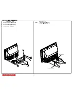
Page 110: ... 4 18 P MJ03587 17 Pcs Ԙ Screws T2B 4 20 P MJ03638 2 Pcs T1T 4 18 P MJ03587 13 Pcs ԙ Screws T2B 4 25 P MJ03639 2 Pcs Ԛ Lower Rear Cover P QD36558 110 CABINET BRACKET BACK FIX METAL QUICK DISASSEMBLE GUIDE QUICK DISASSEMBLE GUIDE TABLE OF CONTENTS ...

Page 111: ... T2B 4 16 P MJ03635 2 Pcs ԙ Lamp Power Unit Ballast P HA01631 Pow Unit Holder P NT03193 Ԛ Side AV Jack Assy P UE35341 Ԛ Ballast FCC Sheet P ME04511 ԛ Screw T2B 4 16 P MJ03635 Ԝ Fan Duct Assy P UX24691 ԝ Screw M3M 3 10 P MJ03601 111 LAMP CONN COVER Put Aluminum Face Down QUICK DISASSEMBLE GUIDE QUICK DISASSEMBLE GUIDE ...

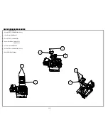
Page 112: ...OPTICAL BLOCK 2 OPTICAL BLOCK 3 Ԙ Front Cover P QD50991 Ԙ Optical Block Assy P UE25321 ԙ Screws T2B 4 16 P MJ03635 2 Pcs 112 QUICK DISASSEMBLE GUIDE QUICK DISASSEMBLE GUIDE ...

Page 113: ...03651 2 Pcs ԙ Lens Barrier P ME04421 Ԛ Screw T3E 3 12 P MJ03651 ԛ Panel Out Ducts P NJ22371 P NJ22361 Ԝ Drive Shield P MD09382 ԝ Screw T3E 3 12 P MJ03651 3 Pcs Ԟ DRIVE PWB P JP08483 113 QUICK DISASSEMBLE GUIDE QUICK DISASSEMBLE GUIDE ...

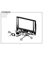
Page 114: ...IRROR COVER ASSY SCREEN FRAME ASSY MIRROR COVER ASSY Ԙ Screws T2B 4 20 P MJ03638 4 Pcs Ԙ Screws T1T 4 18 P MJ03557 14 Pcs ԙ Screws T2B 4 16 P MJ03638 7 Pcs 114 MIRROR COVER ASSY QUICK DISASSEMBLE GUIDE QUICK DISASSEMBLE GUIDE ...

Page 115: ...458 4 Pcs ԙ Screws T1T 4 18 P MJ03587 6 Pcs ԙ Tweeters P GK01401 Ԛ Screws T1T 4 18 P MJ03587 3 Pcs Ԛ Speakers P GK01391 ԛ Mirror P KS09384 ԛ Screws T2B 3 12 P MJ03551 3 Pcs Ԝ Mirror Cover P QD36144 Ԝ LED PWB Assy P JT25003 115 MIRROR RETAINER MIRROR RETAINER MIRROR RETAINER QUICK DISASSEMBLE GUIDE QUICK DISASSEMBLE GUIDE ...

Page 116: ...N FRAME ASSY 2 SCREEN FRAME ASSY 3 Ԙ Screws T1T 4 14 P MJ03588 16 Pcs Ԙ Screen Assy P KR03238 ԙ Screen Frame P QD50981 116 SCREEN FIX METALS SCREEN FIX METALS QUICK DISASSEMBLE GUIDE QUICK DISASSEMBLE GUIDE ...

Page 117: ...CONTROL BLOCK Ԙ Screws T2B 4 16 P MJ03635 2 Pcs ԙ Control Block Assy P UE25331 Ԛ Lamp Cover P PH33036 ԛ Lamp Assy P DP00731 117 LOOSE THIS SCREW LOOSE THESE SCREWS QUICK DISASSEMBLE GUIDE QUICK DISASSEMBLE GUIDE ...

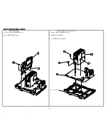
Page 118: ...2503 ԙ Screws T2B 3 12 P MJ03551 4 Pcs Ԛ Control Button P PC06621 Ԛ Nut Washer P MK01431 2 Pcs ԛ Control Panel Frame P PH36821 ԛ Antenna Switch Box P HP00774 Ԝ Screws T2V 4 16 P MJ03442 2 Pcs ԝ Side AV Jack PWB Assy P JT25003 Ԟ AV Jack Frame P PH36452 Plate P PH36801 118 TERMINAL HOLDER QUICK DISASSEMBLE GUIDE QUICK DISASSEMBLE GUIDE ...

Page 119: ...Y DIGITAL CORE Ԙ Screws T2B 3 16 P MJ03459 2 Pcs Ԙ Screws T2B 3 16 P MJ03459 3 Pcs ԙ Powe PWB Assy P JT24993 ԙ Digital Core P UE24613 Ԛ Signal PWB Assy P JT24983 SIGNAL PWB FRAME 119 QUICK DISASSEMBLE GUIDE QUICK DISASSEMBLE GUIDE ...

Page 120: ...ain PR OUT I401 Pin 55 Main PB OUT I401 Pin 56 Main Y OUT I700 Pin 12 Rin1 I700 Pin 10 Gin1 I700 Pin 7 Bin1 1 2 3 4 5 6 7 8 9 I700 Pin 24 VD OUT I700 Pin 25 HD OUT 11 P7A0 F0 K0 Pin 2 DY 10 I700 Pin 31 CLK OUT 12 P7A0 F0 K0 Pin 5 LCCOM Click on number to go to schematic 120 LC57 ...

Page 121: ...0 K0 Pin 22 CLX P7A0 F0 K0 Pin 25 28 ENBX1 4 P7A0 F0 K0 Pin 29 NRG 13 14 15 16 17 18 19 20 21 P7A0 F0 K0 Pin 34 CLY I001 Pin 46 48 ALARM 0 2 23 I902 Pin 3 4 DL OUT 22 I901 Pin 7 8 STBY SWITCHED OUT 24 I902 Pin 1 DL OUT Click on number to go to schematic 121 IMPORTANT NOTE FOR HOT AREA USE AC CORD WITH FLOATING GROUND LC57 ...

Page 122: ...WAVEFORMS AT EACH SECTION PST Pin 63 SDA PST Pin 64 SCL 25 26 Click on number to go to schematic 122 LC57 ...

Page 123: ...e 4 0 Symbol Pin No Voltage Pin No Voltage 24 3 4 54 0 84 0 114 0 PFA3 1 0 5 0 PPT2 1 5 7 11 0 25 0 55 0 85 0 115 0 2 10 1 6 0 2 0 0 12 0 26 0 1 56 4 5 86 0 116 0 3 0 7 0 3 0 0 13 0 27 0 57 4 5 87 0 117 0 4 NC 8 0 4 0 0 14 0 28 0 58 4 5 88 5 6 118 0 5 NC 5 0 15 0 29 0 59 0 89 5 6 119 0 Symbol Pin No Voltage 6 5 7 16 0 30 11 1 60 0 90 5 6 120 0 Symbol Pin No Voltage PTW 1 0 7 5 7 17 5 PFA4 1 0 2 0 ...

Page 124: ... E 0 E 0 Symbol Pin No Voltage Symbol Pin No Voltage Symbol Pin No Voltage Symbol Pin No Voltage Symbol Pin No Voltage Q009 B 0 Q027 B 0 Q501 B 1 5 QA13 B 31 Q943 B 0 8 C 5 C 5 C 0 C 0 C 0 E 0 E 0 E 2 1 E 31 E 0 Symbol Pin No Voltage Symbol Pin No Voltage Symbol Pin No Voltage Symbol Pin No Voltage Symbol Pin No Voltage Q011 B 6 8 Q029 B 5 Q502 B 0 QA14 B 0 Q944 B 0 8 C 0 4 C 0 C 0 C 31 C 0 5 E 7 ...

Page 125: ... 3 3 4 9 2 0 2 0 6 3 3 5 10 Symbol Pin No Voltage Symbol Pin No Voltage Pin No Voltage 3 1 3 3 0 7 0 I903 1 27 3 I7A2 1 5 3 5 10 4 4 3 3 4 0 8 3 3 Symbol Pin No Voltage 2 29 4 2 5 3 6 10 4 5 5 I302 1 2 9 3 0 65 3 5 3 7 0 Symbol Pin No Voltage Pin No Voltage 2 0 4 5 3 4 0 8 15 6 Symbol Pin No Voltage U301 1 0 11 2 7 3 1 3 I591 1 0 2 5 12 3 8 4 5 Symbol Pin No Voltage Symbol Pin No Voltage Pin No Vo...

Page 126: ...gram the value of the parts is subject to be altered for improvement PRODUCT SAFETY NOTE Components marked with a and shaded have special characteristics important to safety Before replacing any of these components read carefully the PRODUCT SAFETY NOTICE of this Service Manual Don t degrade the safety of the receiver through improper servicing BASIC CIRCUIT DIAGRAM TABLE OF CONTENTS 126 ...

Page 127: ...lly the PRODUCT SAFETY NOTICE of this Service Manual Don t degrade the safety of the receiver through improper servicing BASIC CIRCUIT DIAGRAM All DC voltage to be measured with a tester 100k V Voltage taken on a complex color bar signal including a standard color bar signal Since this is a basic circuit diagram the value of the parts is subject to be altered for improvement 127 ...

Page 128: ...gram the value of the parts is subject to be altered for improvement PRODUCT SAFETY NOTE Components marked with a and shaded have special characteristics important to safety Before replacing any of these components read carefully the PRODUCT SAFETY NOTICE of this Service Manual Don t degrade the safety of the receiver through improper servicing BASIC CIRCUIT DIAGRAM TABLE OF CONTENTS 128 ...

Page 129: ...rcuit diagram the value of the parts is subject to be altered for improvement PRODUCT SAFETY NOTE Components marked with a and shaded have special characteristics important to safety Before replacing any of these components read carefully the PRODUCT SAFETY NOTICE of this Service Manual Don t degrade the safety of the receiver through improper servicing BASIC CIRCUIT DIAGRAM 129 ...

Page 130: ...rcuit diagram the value of the parts is subject to be altered for improvement PRODUCT SAFETY NOTE Components marked with a and shaded have special characteristics important to safety Before replacing any of these components read carefully the PRODUCT SAFETY NOTICE of this Service Manual Don t degrade the safety of the receiver through improper servicing BASIC CIRCUIT DIAGRAM 130 ...

Page 131: ...lly the PRODUCT SAFETY NOTICE of this Service Manual Don t degrade the safety of the receiver through improper servicing BASIC CIRCUIT DIAGRAM All DC voltage to be measured with a tester 100k V Voltage taken on a complex color bar signal including a standard color bar signal Since this is a basic circuit diagram the value of the parts is subject to be altered for improvement 131 ...

Page 132: ...rcuit diagram the value of the parts is subject to be altered for improvement PRODUCT SAFETY NOTE Components marked with a and shaded have special characteristics important to safety Before replacing any of these components read carefully the PRODUCT SAFETY NOTICE of this Service Manual Don t degrade the safety of the receiver through improper servicing BASIC CIRCUIT DIAGRAM 132 ...

Page 133: ...m the value of the parts is subject to be altered for improvement PRODUCT SAFETY NOTE Components marked with a and shaded have special characteristics important to safety Before replacing any of these components read carefully the PRODUCT SAFETY NOTICE of this Service Manual Don t degrade the safety of the receiver through improper servicing BASIC CIRCUIT DIAGRAM TABLE OF CONTENTS 1 133 21 ...

Page 134: ...lly the PRODUCT SAFETY NOTICE of this Service Manual Don t degrade the safety of the receiver through improper servicing BASIC CIRCUIT DIAGRAM All DC voltage to be measured with a tester 100k V Voltage taken on a complex color bar signal including a standard color bar signal Since this is a basic circuit diagram the value of the parts is subject to be altered for improvement 134 ...

Page 135: ...m the value of the parts is subject to be altered for improvement PRODUCT SAFETY NOTE Components marked with a and shaded have special characteristics important to safety Before replacing any of these components read carefully the PRODUCT SAFETY NOTICE of this Service Manual Don t degrade the safety of the receiver through improper servicing BASIC CIRCUIT DIAGRAM TABLE OF CONTENTS 135 2 3 4 ...

Page 136: ...it diagram the value of the parts is subject to be altered for improvement PRODUCT SAFETY NOTE Components marked with a and shaded have special characteristics important to safety Before replacing any of these components read carefully the PRODUCT SAFETY NOTICE of this Service Manual Don t degrade the safety of the receiver through improper servicing BASIC CIRCUIT DIAGRAM 136 26 25 ...

Page 137: ...rcuit diagram the value of the parts is subject to be altered for improvement PRODUCT SAFETY NOTE Components marked with a and shaded have special characteristics important to safety Before replacing any of these components read carefully the PRODUCT SAFETY NOTICE of this Service Manual Don t degrade the safety of the receiver through improper servicing BASIC CIRCUIT DIAGRAM 137 ...

Page 138: ...lly the PRODUCT SAFETY NOTICE of this Service Manual Don t degrade the safety of the receiver through improper servicing BASIC CIRCUIT DIAGRAM All DC voltage to be measured with a tester 100k V Voltage taken on a complex color bar signal including a standard color bar signal Since this is a basic circuit diagram the value of the parts is subject to be altered for improvement 138 ...

Page 139: ...c circuit diagram the value of the parts is subject to be altered for improvement PRODUCT SAFETY NOTE Components marked with a and shaded have special characteristics important to safety Before replacing any of these components read carefully the PRODUCT SAFETY NOTICE of this Service Manual Don t degrade the safety of the receiver through improper servicing BASIC CIRCUIT DIAGRAM ...

Page 140: ...e value of the parts is subject to be altered for improvement PRODUCT SAFETY NOTE Components marked with a and shaded have special characteristics important to safety Before replacing any of these components read carefully the PRODUCT SAFETY NOTICE of this Service Manual Don t degrade the safety of the receiver through improper servicing BASIC CIRCUIT DIAGRAM TABLE OF CONTENTS 140 5 6 7 8 9 10 ...

Page 141: ...UCT SAFETY NOTICE of this Service Manual Don t degrade the safety of the receiver through improper servicing BASIC CIRCUIT DIAGRAM All DC voltage to be measured with a tester 100k V Voltage taken on a complex color bar signal including a standard color bar signal Since this is a basic circuit diagram the value of the parts is subject to be altered for improvement 141 11 12 13 16 17 18 19 20 ...

Page 142: ...UCT SAFETY NOTICE of this Service Manual Don t degrade the safety of the receiver through improper servicing BASIC CIRCUIT DIAGRAM All DC voltage to be measured with a tester 100k V Voltage taken on a complex color bar signal including a standard color bar signal Since this is a basic circuit diagram the value of the parts is subject to be altered for improvement 142 11 12 14 16 17 18 19 20 ...

Page 143: ...m the value of the parts is subject to be altered for improvement PRODUCT SAFETY NOTE Components marked with a and shaded have special characteristics important to safety Before replacing any of these components read carefully the PRODUCT SAFETY NOTICE of this Service Manual Don t degrade the safety of the receiver through improper servicing BASIC CIRCUIT DIAGRAM 143 11 12 15 16 17 18 19 20 ...

Page 144: ...lly the PRODUCT SAFETY NOTICE of this Service Manual Don t degrade the safety of the receiver through improper servicing BASIC CIRCUIT DIAGRAM All DC voltage to be measured with a tester 100k V Voltage taken on a complex color bar signal including a standard color bar signal Since this is a basic circuit diagram the value of the parts is subject to be altered for improvement 144 ...

Page 145: ... of the parts is subject to be altered for improvement PRODUCT SAFETY NOTE Components marked with a and shaded have special characteristics important to safety Before replacing any of these components read carefully the PRODUCT SAFETY NOTICE of this Service Manual Don t degrade the safety of the receiver through improper servicing BASIC CIRCUIT DIAGRAM TABLE OF CONTENTS TABLE OF CONTENTS 145 24 23...

Page 146: ...gram the value of the parts is subject to be altered for improvement PRODUCT SAFETY NOTE Components marked with a and shaded have special characteristics important to safety Before replacing any of these components read carefully the PRODUCT SAFETY NOTICE of this Service Manual Don t degrade the safety of the receiver through improper servicing BASIC CIRCUIT DIAGRAM TABLE OF CONTENTS 146 ...

Page 147: ...rcuit diagram the value of the parts is subject to be altered for improvement PRODUCT SAFETY NOTE Components marked with a and shaded have special characteristics important to safety Before replacing any of these components read carefully the PRODUCT SAFETY NOTICE of this Service Manual Don t degrade the safety of the receiver through improper servicing BASIC CIRCUIT DIAGRAM 147 ...

Page 148: ...gram the value of the parts is subject to be altered for improvement PRODUCT SAFETY NOTE Components marked with a and shaded have special characteristics important to safety Before replacing any of these components read carefully the PRODUCT SAFETY NOTICE of this Service Manual Don t degrade the safety of the receiver through improper servicing BASIC CIRCUIT DIAGRAM TABLE OF CONTENTS 148 ...

Page 149: ...4 IR03 C 4 IT04 A 1 DP01 C 2 IT05 A 1 DP02 C 2 IT06 A 1 DP03 C 2 IT07 A 1 DP20 C 2 IT09 A 2 DP21 C 2 IV03 B 4 DPS1 C 3 IV04 C 1 DPS2 C 3 IW01 B 3 DR01 C 4 IW02 A 3 DR02 C 4 IW03 A 3 DR03 C 4 IW05 B 3 DT01 B 1 IW11 A 3 IW12 A 3 IXJ1 C 1 IY01 B 3 XP01 C 3 IY02 B 3 XP05 C 2 IY03 B 3 XPS1 C 3 XT01 B 2 XT02 B 2 XT03 A 1 QP01 C 2 XT06 B 1 QP02 C 2 XT07 B 1 QP08 C 3 XY01 C 3 QR01 C 4 XY02 B 4 CRYSTAL FIL...

Page 150: ...8 A 3 QW02 B 2 IT13 B 4 QX01 C 2 IV01 B 1 QX02 C 2 IV02 B 1 QX03 C 2 IV05 B 2 QY01 C 2 IW04 A 3 QY02 C 2 IW06 A 3 IW07 B 3 IW08 B 2 IW09 B 2 XP04 A 2 IW10 B 2 XP06 C 3 IYJ2 B 2 XT04 A 4 XT05 B 4 XV01 B 1 XX05 C 4 QM01 C 4 XX06 C 4 QM02 C 3 XX07 C 3 CRYSTAL FILTER IC TRANSISTOR PRINTED CIRCUIT BOARDS LC57 SUBDIGITAL PWB Solder side BACK TO TABLE OF CONTENTS LC57 1 2 3 4 A B C 150 ...

Page 151: ...QJ00 A 3 DF06 A 2 Q007 B 2 QJ01 A 3 DF07 A 3 Q008 B 2 QJ02 A 3 DF08 A 3 Q009 A 2 QJ03 A 3 DJ00 A 3 Q010 B 2 QJ04 A 3 DJ01 A 3 Q011 B 2 QJ05 C 3 DJ02 C 3 Q012 B 2 QJ06 A 3 DJ03 C 3 Q013 B 2 DJ04 A 4 Q014 B 2 DJ07 A 4 Q015 B 2 DJ08 A 3 Q016 B 2 D001 A 1 DJ09 A 3 Q017 B 2 D002 A 2 DJ10 A 4 Q018 A 2 D003 A 2 DJ11 A 4 Q021 B 2 D004 A 2 DJ12 A 4 Q022 A 1 D005 B 2 DJ13 C 3 Q023 A 1 D006 B 2 DJ14 A 3 Q024...

Page 152: ...LC57 SIGNAL PWB Solder side PRINTED CIRCUIT BOARDS BACK TO TABLE OF CONTENTS LC57 152 ...

Page 153: ... C I602 B 2 I603 B 1 I606 B 2 I607 B 2 I700 A 4 I750 A 3 I7A0 C 1 I7A2 B 1 I7F0 A 2 I7K0 C 4 I7K1 B 4 I7K3 B 4 I7K4 B 4 I7K5 B 3 I800 A 1 I801 B 4 I802 B 4 I803 B 4 I804 A 1 I808 A 1 Q7F0 A 2 Q7F1 A 2 D610 A 1 X607 A 1 FILTER DIODE IC TRANSISTOR DRIVE PWB SEMICONDUCTOR LOCATION Component Side 153 ...

Page 154: ... 1 Q7K3 B 1 Q7K4 B 2 D613 B 3 D7A0 A 2 D7A1 A 2 D801 B 1 D804 B 1 D805 A 4 D806 A 4 X604 B 4 X605 B 3 X606 A 4 X608 A 3 X609 A 3 X610 A 3 X611 A 3 X612 A 3 X613 A 3 X614 A 3 X615 A 3 X616 A 3 X617 A 3 X700 A 1 X702 A 1 X703 A 2 X704 A 2 X800 A 4 X801 A 4 X802 A 4 X803 A 4 X804 A 4 X805 A 4 IC CRYSTAL FILTER TRANSISTOR DIODE DRIVE PWB SEMICONDUCTOR LOCATION Solder Side 154 ...

Page 155: ...D943 A 4 I942 A 3 D944 A 3 D945 B 4 D946 B 4 D947 B 4 Q901 A 3 D948 B 4 Q942 A 3 D949 A 3 Q943 A 4 D950 C 4 Q944 B 4 D951 C 4 Q980 D 4 D952 A 3 Q981 D 4 D953 B 4 Q982 D 3 D954 C 4 D955 C 4 D958 C 4 D959 A 3 D901 B 2 D962 A 2 D902 B 1 D988 C 4 D903 A 1 D990 C 4 D904 B 3 D991 D 3 D906 B 2 D907 B 2 D909 B 2 D910 D 2 X901 D 1 D911 D 2 X902 D 1 D912 D 1 IC TRANSISTOR DIODE CRYSTAL FILTER POWER PWB SEMI...

Page 156: ...PRINTED CIRCUIT BOARDS LC57 POWER PWB Solder side BACK TO TABLE OF CONTENTS LC57 156 ...

Page 157: ...PRINTED CIRCUIT BOARDS LC57 SENSOR PWB BACK TO TABLE OF CONTENTS LC57 Component side DL02 IC DIODE IL01 DL01 Component side Solder side 157 ...

Page 158: ...PRINTED CIRCUIT BOARDS LC57 AV JACK PWB Component side Solder side BACK TO TABLE OF CONTENTS LC57 Component side QM14 DM10 QM15 QM04 QM13 DIODE TRANSISTOR DM09 QM03 DM07 DM08 158 ...

Page 159: ...PRINTED CIRCUIT BOARDS LC57 DOOR SW A PWB Component side Solder side BACK TO TABLE OF CONTENTS LC57 159 ...

Page 160: ...PRINTED CIRCUIT BOARDS LC57 DOOR SW B PWB BACK TO TABLE OF CONTENTS LC57 Component side Solder side 160 ...

Page 161: ...PRINTED CIRCUIT BOARDS LC57 IR SUB PWB BACK TO TABLE OF CONTENTS LC57 DM13 DM14 DM15 DM16 HM02 QM06 QM07 QM08 IC TRANSISTOR IM01 DIODE Component side Component side Solder side 161 ...

Page 162: ...M01 DM02 DM03 DM04 DM05 DM11 DM12 DM18 DM19 HM01 QM01 QM05 QM10 QM11 QM12 TRANSISTOR DIODE PRINTED CIRCUIT BOARDS LC57 LED PWB BACK TO TABLE OF CONTENTS LC57 Component side Solder side Component side 162 ...

Page 163: ...PRINTED CIRCUIT BOARDS LC57 PJIG B PWB Solder side BACK TO TABLE OF CONTENTS LC57 Component side 163 ...

Page 164: ...PRINTED CIRCUIT BOARDS LC57 TACT SW PWB BACK TO TABLE OF CONTENTS LC57 Component side Solder side 164 ...

Page 165: ...R CAP CHIP CERAMIC 10UF 10V 2012BK 0 CP20 AA00937R CAP CHIP CERAMIC 10UF 10V 2012BK 0 CT22 0893179R CAP CHIP CERAMIC 100000PF 16V TAPE 0 CP21 0893179R CAP CHIP CERAMIC 100000PF 16V TAPE 0 CT23 0893208R CAP 1608CHIP 1000PFKB 50V TAPE 0 CP22 0893179R CAP CHIP CERAMIC 100000PF 16V TAPE 0 CT24 AA01111R CERAMIC CAPACITOR 1 0UF 6 3V 0 CP23 AA00969R CAP CHIP2125 B 22UF6 3V 0 CT25 AA00937R CAP CHIP CERAMI...

Page 166: ...0000PF 16V TAPE 0 CT89 AA01231R 0 1UF 16V 1005 B CERAMIC CAPAC 0 CTK3 0893179R CAP CHIP CERAMIC 100000PF 16V TAPE 0 CT90 AA01231R 0 1UF 16V 1005 B CERAMIC CAPAC 0 CTK4 AA00937R CAP CHIP CERAMIC 10UF 10V 2012BK 0 CT91 AA01231R 0 1UF 16V 1005 B CERAMIC CAPAC 0 CTK6 0893179R CAP CHIP CERAMIC 100000PF 16V TAPE 0 CT92 AA01231R 0 1UF 16V 1005 B CERAMIC CAPAC 0 CTK7 0893179R CAP CHIP CERAMIC 100000PF 16V...

Page 167: ...889R LBC2518 CHIP COIL 22UH 0 LX02 BA00889R LBC2518 CHIP COIL 22UH 0 MODULES HM01 CZ01241 GP1FM514TZ0F 0 TRANSISTORS QM04 CA02091R SRC1204EF_PF 0 INTEGRATED CIRCUITS IC s QP08 CA02091R SRC1204EF_PF 0 IM01 CK37218R MONO IC TK11150CSCL 0 QT01 CA02171R TRS CHIP 2SC4082T106P 0 IM02 CK50961R SN74CB3T3306DCUR 0 QT02 CA02171R TRS CHIP 2SC4082T106P 0 IM03 CK38326R IC SN74LVC1G32DCKR 0 QT03 CA02171R TRS CH...

Page 168: ...23 AQ00244R RES CHIP 1 16W 75K OHM TAPE 0 RW42 0790051R RES CHIP 1 16W 10K OHM 0 RT24 0790046R RES CHIP 1 16W 4 7K OHM 0 RW43 AZ01031R THERMISTOR NANOSMDC050F13 2 0 RT25 0790046R RES CHIP 1 16W 4 7K OHM 0 RW44 0790019R RES CHIP 1 16W 47 OHM 0 RT26 0790001R CHIP RESISTOR RECJUMPER 1 16C16T1608 0 RW45 0790019R RES CHIP 1 16W 47 OHM 0 RT27 0790024R RES CHIP 1 16W 100 OHM 0 RW47 0790001R CHIP RESISTOR...

Page 169: ...CCC105K10 B 16CT 0 CAPACITORS C412 AA01123R CCC105K10 B 16CT 0 C004 AA01123R CCC105K10 B 16CT 0 C413 AA01141R CERAMIC CAPACITOR 0 1UF 16V 0 C006 AA01123R CCC105K10 B 16CT 0 C414 AA01123R CCC105K10 B 16CT 0 C007 0800326R CAP ELECTRO 100UF M 16V 0 C415 AA01123R CCC105K10 B 16CT 0 C008 AA01141R CERAMIC CAPACITOR 0 1UF 16V 0 C416 AA01141R CERAMIC CAPACITOR 0 1UF 16V 0 C010 0893208R CAP 1608CHIP 1000PF...

Page 170: ...4R CAP POLYESTER 0 1UF J 50V 0 DJ23 2348101M ZENER MTZJ 5 1A TA 0 CA57 0880194R CAP POLYESTER 0 1UF J 50V 0 DJ25 2348101M ZENER MTZJ 5 1A TA 0 CA59 AL01152S CAP ELECTROLYTIC 470UF M YXF 3 0 DP01 2342062 DIODE D3SBA60 4103 0 CA60 0284824F CAP ELECTRO 2200UF 35V 0 CA61 0284824F CAP ELECTRO 2200UF 35V 0 PROTECTORS CA64 258616 CAP ELECTRO 2 2UF M 50V 0 FE01 2721351 FUSE HOLDER 0 CA65 258616 CAP ELECTR...

Page 171: ...CA02132R TRS CHIP 2SA1980UFG_PF 0 R070 0790033R RES CHIP 1 16W 470 OHM 0 Q407 CA02132R TRS CHIP 2SA1980UFG_PF 0 R071 0790051R RES CHIP 1 16W 10K OHM 0 Q408 CA02132R TRS CHIP 2SA1980UFG_PF 0 R074 0790001R CHIP RESISTOR RECJUMPER 1 16C16T1608 0 Q409 CA02132R TRS CHIP 2SA1980UFG_PF 0 R075 0790051R RES CHIP 1 16W 10K OHM 0 Q410 CA02132R TRS CHIP 2SA1980UFG_PF 0 R076 0790051R RES CHIP 1 16W 10K OHM 0 Q...

Page 172: ...7 AQ00164R CHIP RESISTOR 1 16W 75OHM TAPE 0 R183 0790037R RES CHIP 1 16W 1 0K OHM 0 R448 0790024R RES CHIP 1 16W 100 OHM 0 R184 0790037R RES CHIP 1 16W 1 0K OHM 0 R449 0790024R RES CHIP 1 16W 100 OHM 0 R185 0790037R RES CHIP 1 16W 1 0K OHM 0 R450 0790024R RES CHIP 1 16W 100 OHM 0 R186 0790037R RES CHIP 1 16W 1 0K OHM 0 R451 0790024R RES CHIP 1 16W 100 OHM 0 R187 0790037R RES CHIP 1 16W 1 0K OHM 0 ...

Page 173: ...001R CHIP RESISTOR RECJUMPER 1 16C16T1608 0 R546 0790028R RES CHIP 1 16W 220 OHM 0 RF16 0790001R CHIP RESISTOR RECJUMPER 1 16C16T1608 0 R547 0790001R CHIP RESISTOR RECJUMPER 1 16C16T1608 0 RF17 0790037R RES CHIP 1 16W 1 0K OHM 0 R548 0790001R CHIP RESISTOR RECJUMPER 1 16C16T1608 0 RF18 AQ00196R RES CHIP 1 16W 1 2K OHM TAPE 0 R550 0790001R CHIP RESISTOR RECJUMPER 1 16C16T1608 0 RF21 0790001R CHIP R...

Page 174: ...S PPDE ED02813 4P VH CONNECTOR PLUG 2 4 NC 0 D901 CH00051 DIODE SD S1WB A 60B 600V 0 PPL 2674281 3P B PLUG PIN 0 D902 2342061 DIODE D3SB A 60 0 PPT1 ED03203 6P 2 5MM PITCH CONNECTOR TAC L06X A3 0 D903 CH02001M DIODE 1SR139 400 0 PPT2 ED04332U 2 54MM PITCH 20P B TO B CONNEC 0 D906 CH02011M DIODE 1SR153 400 0 PPT3 ED04332U 2 54MM PITCH 20P B TO B CONNEC 0 D907 2348113M DIO MTZ J5 6CTA 0 PSP1 ED00387...

Page 175: ...JUMP WIRE 0 R927 0700054M RES CARBON FLM 1 16W 10K JB 0 K023 2784381M 0 60MM TAPED JUMP WIRE 0 R928 AT03665M RES MTL GRAZD FLM 1 2W 1M 0 K024 2784381M 0 60MM TAPED JUMP WIRE 0 R929 AT03665M RES MTL GRAZD FLM 1 2W 1M 0 K025 2784381M 0 60MM TAPED JUMP WIRE 0 R940 0700063M RES CARBON FLM 1 16W 47K JB 0 K026 2784381M 0 60MM TAPED JUMP WIRE 0 R941 0700063M RES CARBON FLM 1 16W 47K JB 0 K027 2784381M 0 ...

Page 176: ... 0893222R CAP 1608CHIP10000PFKB 50V TAPE 0 C621 AD00623R CEC101M06 EWMT 105 0 C7G2 0893222R CAP 1608CHIP10000PFKB 50V TAPE 0 C622 0893232R CAP 1608CHIP 100000PFZF25V TAPE 0 C7G4 AA01347R CERAMIC CAPACITOR 0 1UF 25V B 0 C623 AD00623R CEC101M06 EWMT 105 0 C7G5 AA01347R CERAMIC CAPACITOR 0 1UF 25V B 0 C624 0893232R CAP 1608CHIP 100000PFZF25V TAPE 0 C7G6 AA01347R CERAMIC CAPACITOR 0 1UF 25V B 0 C625 A...

Page 177: ...16C16T1608 0 I7K1 CK18641R IC BA10358F E2 T1 0 R668 0790001R CHIP RESISTOR RECJUMPER 1 16C16T1608 0 I7K3 CK18641R IC BA10358F E2 T1 0 R669 0790001R CHIP RESISTOR RECJUMPER 1 16C16T1608 0 I800 CK38379R ANALOG MONO SI 3010KM TL 0 R670 0790001R CHIP RESISTOR RECJUMPER 1 16C16T1608 0 I801 CK38379R ANALOG MONO SI 3010KM TL 0 R673 0790024R RES CHIP 1 16W 100 OHM 0 I802 CK38372R DIGITAL MONO IC SI 3018KM...

Page 178: ... OHM 0 R7M8 0790051R RES CHIP 1 16W 10K OHM 0 R760 0790024R RES CHIP 1 16W 100 OHM 0 R7M9 0790051R RES CHIP 1 16W 10K OHM 0 R766 0790001R CHIP RESISTOR RECJUMPER 1 16C16T1608 0 R7N0 0790051R RES CHIP 1 16W 10K OHM 0 R767 0790001R CHIP RESISTOR RECJUMPER 1 16C16T1608 0 R7N3 0790052R RES CHIP 1 16W 12K OHM 0 R768 AQ00228R RES CHIP 1 16W 20K OHM TAPE 0 R7N4 0790039R RES CHIP 1 16W 1 5K OHM 0 R770 079...

Page 179: ...04 3631 0 QM04 CF02981R 2SC5343YT_PF 0 PDD EA02421U 30P LVDS IF CONNECTER 0 QM05 CF02981R 2SC5343YT_PF 0 PDE EA02132R 3P SMT PH CONNE POST LF 0 QM10 CF02981R 2SC5343YT_PF 0 PDJ EA02136R 7P SMT PH CONNE POST LF 0 QM11 CF02981R 2SC5343YT_PF 0 PDP EA02139R 10P SMT PH CONNE POST LF 0 QM12 CF02981R 2SC5343YT_PF 0 PDT EA02141R 11P SMT PH CONNE POST LF 0 PSL EA02135R 6P SMT PH CONNE POST LF 0 RESISTORS R...

Page 180: ... CONNECTOR 750MM 0 CAPACITORS ETW EF23315 5P PH PH CONNECTOR 1300 800MM 0 CL01 AA01141R CERAMIC CAPACITOR 0 1UF 16V 0 EUSB EW08451 4J USB CABLE L 1 0 ESPL EF24872 5J SMP FASTON CONNECTOR 2100 1 0 DIODES ESPR EF24881 4J SM FASTON CONNECTOR 750 600 0 DL01 CC00144R CHIP DIODE RD5 6UM B T 0 EFF2 EF03231S 5P CONNECTOR L 180 0 DL02 CC00144R CHIP DIODE RD5 6UM B T 0 EFT EF20973 13P XA CONNECTOR 220MM 0 I...

Page 181: ...OPOUT 5V 3 3 V REGULATOR FOR POD IF SUBDIGITAL 0 31 IW07 CK38326R IC SN74LVC1G32DCKR SINGLE 2 INPUT POSITIVE OR GATE SUBDIGITAL 0 32 IW08 CK38917R DIGITAL MONOLITHIC IC SN74LVC32APWR QUADRUPLE 2 INPUT POSITIVE OR GATES SUBDIGITAL 0 33 IW09 CK36321R SN74LVC125APW QUADRUPLE BUS BUFFER GATE WITH 3 STATE OUT POD IF SUBDIGITAL 0 34 IW10 CK08271R DIGITAL MONOLITHIC IC SN74LVC244PW OCTAL BUFFER DRIVER WI...

Page 182: ...LTAGE REGULATOR DRIVE 0 76 I802 CK38372R DIGITAL MONO IC SI 3018KM LOW DROPOUT 1 8 V VOLTAGE REGULATOR DRIVE 0 77 I803 CK38375R DIGITAL MONO IC SI 3033KM LOW DROPOUT 3 3 V VOLTAGE REGULATOR DRIVE 0 78 I804 CK37193R MONO IC SI 3033LSA TL LOW VOLTAGE HIGH CURRENT 3 3 V LINEAR REGULATOR DRIVE 0 79 I808 CK38375R DIGITAL MONO IC SI 3033KM 1 A LOW DROPOUT 3 3 V VOLTAGE REGULATOR DRIVE 0 80 DM15 CH02721 ...

Page 183: ......
Reviews: