11
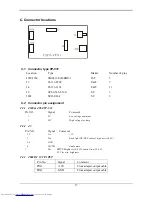
F-3 CN2
Terminal No. Symbol
Function
Terminal No. Symbol
Function
1
VDD2
Analog Power Input (DC+9V)
31
POL
Source Driver Output
Polarity Control
2
VDD2
Analog Power Input (DC+9V)
32
REV
Data Reverse Control Signal
3 GND
Ground
33 GND Ground
4 GND
Ground
34 GND Ground
5
EB5
Even-dot Blue Data bit 5(MSB)
35
STV1
Vertical start Pulse1
6
EB4
Even-dot Blue Data bit 4
36
STV2
Vertical start Pulse2
7
EB3
Even-dot Blue Data bit 3
37
CPV
Vertical Clock Input
8
EB2
Even-dot Blue Data bit 2
38
OE
Gate Driver Output Enable
Signal
9
EB1
Even-dot Blue Data bit 1
39
GND
Ground
10
EB0
Even-dot Blue Data bit 0 (LSB)
40
GND
Ground
11 GND
Ground
12
EG5
Even-dot Green Data bit 5 (MSB)
13
EG4
Even-dot Green Data bit 4
14
EG3
Even-dot Green Data bit 3
15
EG2
Even-dot Green Data bit 2
16
EG1
Even-dot Green Data bit 1
17
EG0
Even-dot Green Data bit 0 (LSB)
18 GND
Ground
19
ER5
Even-dot Red Data bit 5 (MSB)
20
ER4
Even-dot Red Data bit 4
21
ER3
Even-dot Red Data bit 3
22
ER2
Even-dot Red Data bit 2
23
ER1
Even-dot Red Data bit 1
24
ER0
Even-dot Red Data bit 0 (LSB)
25 GND
Ground
26
CPH1
Pixel Clock Input
27 GND
Ground
28 GND
Ground
29
STH
Horizontal start Pulse
30
LOAD
Source Driver Latch Pulse
Summary of Contents for CML153
Page 26: ...22 10 TROUBLESHOOTING A Main Procedure ...
Page 27: ...23 A 1 Power Circuit Troubleshooting ...
Page 28: ...24 A 2 Backlights Troubleshooting ...
Page 29: ...25 A 3 Performance Troubleshooting ...
Page 30: ...26 A 4 Function Troubleshooting ...
Page 31: ...27 APPENDIX A Display Unit Assembly ...
Page 32: ...28 ...
Page 33: ...29 APPENDIX B PCB ASSEMBLY ...
Page 34: ...30 ...
Page 35: ...31 ...
Page 36: ...32 ...
Page 37: ...33 ...
Page 38: ...34 ...
Page 39: ......
Page 40: ...36 ...


