background image

Service manual CL2554AN / CL2854AN

- 28 -

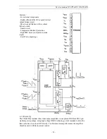
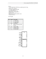
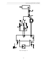
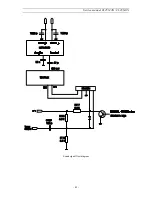
Features :

- Few external components

- Highly efficient fully DC-coupled vertical

output bridge circuit

- Short rise and fall time of the vertical

flyback switch

- Guard circuit

- Temperature (thermal) protection

- High EMC because of common mode

inputs

- East-West output stage

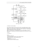
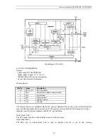
4-5 TDA6107Q

The TDA6107Q includes three video output amplifiers in one plastic DIL-Bent-SIL 9-pin

medium power package, using high voltage DMOS technology, and is intended to drive the

three cathodes of a colour CRT directly. To obtain maximum performance, the amplifier

should be used with black-current control.

Summary of Contents for CL2554AN

Page 1: ... sécurité et les Notices de sécurité du produit présentés dans le présent manuel VORSICHT Vor Öffnen des Gehäuses hat der Service Ingenieur die Sicherheitshinweise und Hinweise zur Produktsicherheit in diesem Wartungshandbuch zu lesen Data contained within this Service manual is subject to alteration for improvement Les données fournies dans le présent manuel d entretien peuvent faire l objet de m...

Page 2: ...text decoder with embedded m Controller 4 2 MSP3415D Multistandard Sound Processor 4 3 TDA894xJ Stereo Audio Amplifier 4 4 TDA835xJ Vertical Amplifier 4 4 1 TDA8357J 4 4 1 TDA8358J 4 5 TDA6107Q 4 6 24C08 8 Kbit EEPROM 4 7 STR F6653 5 Circuit description 5 1 Block diagram 5 2 IF 5 3 Source switching 5 4 m Controller I O pin configuration and function 5 5 Sound processing 5 6 Sound amplification 5 7...

Page 3: ...Screen Display Program Selection 100 programmes Aux terminal EURO SCART 1 Audio Video In and Out R G B In Slow and Fast switching EURO SCART 2 Audio Video In SVHS In Audio Video Jack on front of cabinet in common connection with EURO SCART 2 Headphone jack 3 5 mm on front of cabinet Remote Control Unit R 40A01 21 Pin EURO SCART 1 Pin Signal Description Matching value 1 Audio Output Right 0 5 Vrms ...

Page 4: ...ideo Input 1 Vpp 3dB Impedance 75W 21 Common Earth 21 Pin EURO SCART 2 Pin Signal Description Matching value 1 N C 2 Audio Input Right 0 5 Vrms Impedance 10 kW 3 N C 4 Audio Earth 5 Earth 6 Audio Input Left 0 5 Vrms Impedance 10 kW 7 N C 8 N C 9 N C 10 N C 11 N C 12 N C 13 Earth 14 Earth 15 Chroma Input 3dB for a luminance signal of 1 Vpp 16 N C 17 Earth 18 Video In Earth 19 N C 20 Video Input Y I...

Page 5: ... 201 25 C20 C21 471 25 471 25 471 25 471 25 C22 479 25 479 25 479 25 479 25 C23 487 25 487 25 487 25 487 25 C24 495 25 495 25 495 25 495 25 C25 503 25 503 25 503 25 503 25 C26 511 25 511 25 511 25 511 25 C27 519 25 519 25 519 25 519 25 C28 527 25 527 25 527 25 527 25 C29 535 25 535 25 535 25 535 25 C30 543 25 543 25 543 25 543 25 C31 551 25 551 25 551 25 551 25 C32 559 25 559 25 559 25 559 25 C33 ...

Page 6: ...815 25 815 25 C65 823 25 823 25 823 25 823 25 C66 831 25 831 25 831 25 831 25 C67 839 25 839 25 839 25 839 25 C68 847 25 847 25 847 25 847 25 C69 855 25 855 25 855 25 855 25 C70 863 25 863 25 863 25 863 25 C71 69 25 C72 76 25 C73 83 25 C74 90 25 C75 97 25 C76 59 25 C77 93 25 S01 105 25 104 75 103 25 105 25 S02 112 25 116 75 111 25 112 25 S03 119 25 128 75 119 25 119 25 S04 126 25 140 75 127 25 126...

Page 7: ...351 25 351 25 351 25 351 25 S28 359 25 359 25 359 25 359 25 S29 367 25 367 25 367 25 367 25 S30 375 25 375 25 375 25 375 25 S31 383 25 383 25 383 25 383 25 S32 391 25 391 25 391 25 391 25 S33 399 25 399 25 399 25 399 25 S34 407 25 407 25 407 25 407 25 S35 415 25 415 25 415 25 415 25 S36 423 25 423 25 423 25 423 25 S37 431 25 431 25 431 25 431 25 S38 439 25 439 25 439 25 439 25 S39 447 25 447 25 44...

Page 8: ...IV If two or more programs with the same code are found only the strongest or if they have the same level the one with the lowest frequency is listed in group I II or III The others are listed in group IV Note If two programs with the same name but a different code are found these two programs are listed in group I II or III e g Regional program SW3 in Germany The sorting order within group II III...

Page 9: ...If GB is selected the TV controlling software seeks for programs only in UHF C21 to C70 The sorting order is 1 BBC1 2 BBC2 3 ITV 4 CH4 5 CH5 6 NEWS If two or more identical programs same name but different code e g BBC1 and BBC1 Scotland are found the following programs in the list will be shifted up 1 BBC1 2 BBC1 3 BBC2 4 ITV 5 CH4 6 CH5 7 NEWS If one of the program above is not found the associa...

Page 10: ...en working on high voltage equipment 2 Discharge the high potential of the picture tube before handling the tube The picture tube is highly evacuated and if broken glass fragments will be violently expelled 2 If any Fuse in this TV receiver is blown replace it with the FUSE specified in the Replacement Parts List 3 When replacing a high wattage resistor oxide metal film resistor in circuit board k...

Page 11: ...WOO SAMSUNG 140V 92V 1 DAEWOO SAMSUNG 2 SIEL 140V 92V 3 3 TV set Alignment 3 3 1 G2 alignment TV in AV mode without video signal Þ Black screen TV pre set with WP Red WP Green and WP Blue equal to 32 TV pre set with Black R Black G equal to 8 Set TV in NORMAL I mode Adjust screen volume on FBT such that the highest cathode cut off voltage measured on CRT board is V cut off 5V Screen size V cut off...

Page 12: ...ntring Adjust H Shift to have the picture in the centre of the screen 3 3 6 East West correction Adjust the H Parall H Bow H Width EW Parabo Up Corner Dw Corner EW trapez to compensate for geometrical distortion H Parall H Bow H Width EW Parabo Up Corner Dw Corner ...

Page 13: ...ice manual CL2554AN CL2854AN 12 EW Trapez 3 3 7 AGC Adjust the antenna signal level at 68 dBmV 2 UHF CH25 Set RF AGC to 0 Increase RF AGC level and stop when the level on pin 6 of TDA936x goes below 2 5 Vdc ...

Page 14: ...th fast blanking for external RGB YUV sources The Text OSD signals are internally supplied from the m Controller Teletext decoder l Contrast reduction possibility during mixed mode of OSD and Text signals l Horizontal synchronisation with two control loops and alignment free horizontal oscillator l Vertical count down circuit l Vertical driver optimised for DC coupled vertical output stages l Hori...

Page 15: ...able scan lines per row 9 10 13 16 and character matrix 12x10 12xl3 12x16 VxH l Fringing Shadow selectable from N S E W direction l Fringe colour selectable l Meshing of defined area l Contrast reduction of defined area l Cursor l Special Graphics Characters with two planes allowing four colours per character l 32 software re definable On Screen display characters l 4 WST Character sets GO G2 in s...

Page 16: ...I Real time capture and decoding for WST Teletext in Hardware to enable optimised microprocessor throughput 10 pages stored On Chip Inventory of transmitted Teletext pages stored in the Transmitted Page Table TPT and Subtitle Page Table SPT Automatic detection of FASTEXT transmission Real time packet 26 engine in Hardware for processing accented G2 and G3 characters Signal quality detector for WST...

Page 17: ...Service manual CL2554AN CL2854AN 16 ...

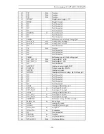
Page 18: ...orwegian Swedish GB France Germany Belgium Spain Italy Switzerland Austria Denmark Finland Netherlands Norway Sweden Ireland Others Pan European West DW9365 N1 3 BDx note x is the software version English Polish Russian Hungarian Czech Slovakian Romanian Greek Poland Hungary Czech rep Others Pan European East Cyrillic Greek PINNING SYMBOL PIN DESCRIPTION n u 1 Port 1 3 Not used SCL 2 I2C bus clock...

Page 19: ... GND2 30 ground 2 for TV processor SIF AGC 31 AGC sound IF REF0 32 n u HOUT 33 horizontal output FBISO 34 flyback input sandcastle output QSS out 35 QSS intercarrier output EHT0 36 EHT Overvoltage protection PLLIF 37 IF PLL loop filter IFVO 38 IF video output VP1 39 main supply voltage TV processor CVBSINT 40 internal CVBS input GND1 41 ground 1 for TV processor CVBS Y 42 external CVBS Y input CHR...

Page 20: ...N 19 XTALOUT 59 crystal oscillator output RESET 60 reset VDDP 61 digital supply to periphery 3 3V Audio Mute 62 Port 1 0 Audio mute output PushPull Power 63 Port 1 1 Power output PushPull IR in 64 Interrupt input 0 R C Infrared input ...

Page 21: ...Service manual CL2554AN CL2854AN 20 ...

Page 22: ...r Section The MSP 3415D is designed to simultaneously perform digital demodulation and decoding of NICAM coded TV stereo sound as well as demodulation of FM or AM mono TV sound Alternatively two carrier FM systems according to the German terrestrial specs can be processed with the MSP 3415D The MSP 3415D facilitates profitable multistandard capability offering the following advantages Automatic Ga...

Page 23: ...h quality digital sound channels to be added to the already existing FM AM channel The sound coding follows the format of the so called Near Instantaneous Companding System NICAM 728 Transmission is performed using Differential Quadrature Phase Shift Keying DQPSK Table below offers an overview of the modulation parameters In the case of NICAM FM AM mode there are three different audio channels ava...

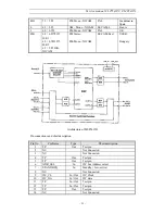
Page 24: ...M SECAM East USSR Hungary Architecture of MSP3415D Pin connections and short description Pin No Pin Name Type Short description 1 TP Out Test pin 2 NC Not Connected 3 NC Not Connected 4 TP Out Test pin 5 TP Out Test pin 6 ADR_SEL In I2C bus Address select 7 STANDBYQ In Standby Low active 8 NC Not Connected 9 I2C_CL In Out I2C Clock 10 I2C_DA In Out I2C data 11 TP In Out Test pin 12 TP In Out Test ...

Page 25: ...SC1_OUT_L Out Scart output 1 left 38 NC Not Connected 39 AHVSUP Analogue power supply 8 0V 40 CAPL_M Volume capacitor MAIN 41 AHVSS Analogue ground 42 AGNDC Analogue reference voltage high voltage part 43 NC Not Connected 44 NC Not Connected 45 NC Not Connected 46 NC Not Connected 47 NC Not Connected 48 ASG2 Analogue Shield Ground 2 49 SC2_IN_L In Scart input 2 in left 50 SC2_IN_R In Scart input 2...

Page 26: ...al components Fixed gain Standby and mute mode No on off switching plops low standby current High supply voltage ripple rejection Outputs short circuit protected to ground supply and across the load Thermally protected Pin description Pin Symbol Description 1 OUT1 negative loudspeaker terminal 1 2 GND1 ground channel 1 3 Vcc1 supply voltage channel 1 4 OUT1 positive loudspeaker terminal 1 5 n c no...

Page 27: ...t class G system Due to the full bridge output circuit the deflection coils can be DC coupled The IC is constructed in a Low Voltage DMOS process that combines Bipolar CMOS and DMOS devices MOS transistors are used in the output stage because of the absence of second breakdown 4 4 1 TDA8357J Features Few external components Highly efficient fully DC coupled vertical output bridge circuit Short ris...

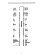
Page 28: ... input voltage negative 3 Vp supply voltage 4 VOB output voltage B 5 GND ground 6 Vflb flyback supply voltage 7 VOA output voltage A 8 VO guard guard output voltage 9 VM input measuring resistor 4 4 1 TDA8358J An East West output stage is provided that is able to sink current from the diode modulator circuit ...

Page 29: ...t Temperature thermal protection High EMC because of common mode inputs East West output stage 4 5 TDA6107Q The TDA6107Q includes three video output amplifiers in one plastic DIL Bent SIL 9 pin medium power package using high voltage DMOS technology and is intended to drive the three cathodes of a colour CRT directly To obtain maximum performance the amplifier should be used with black current con...

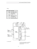
Page 30: ...pply voltage of 200V Internal reference voltage of 2 5 V Fixed gain of 50 Black current stabilisation BCS circuit Thermal protection Pin description Pin Symbol Description 1 Vi 1 inverting input 1 2 Vi 2 inverting input 2 3 Vi 3 inverting input 3 4 GND ground fin 5 Iom black current measurement output 6 VDD supply voltage 7 VOC 3 cathode output 3 8 VOC 2 cathode output 2 9 VOC 1 cathode output 1 ...

Page 31: ... Output 6 SCL Serial clock 7 WC Write control 8 Vcc Supply voltage 4 Vss Ground The memory device is compatible with the I2C memory standard This is a two wire serial interface that uses a bi directional data bus and serial clock The memory carries a built in 4 bit unique device type identifier code 1010 in accordance with the I2C bus definition Serial Clock SCL The SCL input is used to strobe all...

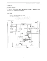
Page 32: ...SFET and control IC designed for flyback converter type switch mode power supply applications 4 7 2 Features Small SIP fully isolated molded 5 pins package Many protection functions Pulse by pulse overcurrent protection OCP Overvoltage protection with latch mode OVP Thermal protection with latch mode TSD 4 7 3 Block diagram ...

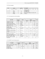
Page 33: ... TOFF max 45 55 msec Minimum time for input of quaxi resonant signals 1 5 TTH 2 1 0 msec Minimum off time TOFF min 1 5 msec O C P F B terminal threshold voltage 1 1 5 VTH 1 0 68 0 73 0 78 V O C P F B terminal threshold voltage 2 1 5 VTH 2 1 3 1 45 1 6 V O C P F B terminal extraction current 1 2 IOCP FB 1 2 1 35 1 5 mA O V P operation voltage 4 5 VIN OVP 20 5 22 5 24 5 V Latch circuit sustaining vo...

Page 34: ...Service manual CL2554AN CL2854AN 33 5 Circuit description 5 1 Block diagram ...

Page 35: ...high performance hi fi stereo sound processing can be achieved Video switches The video switch has one input for an external CVBS or Y C signal The selected CVBS signal can be supplied to pin 38 the IF video output The selection between both signals is realised by the controlling software in subaddress 22H The video ident circuit is connected to the selected signal This ident circuit is independen...

Page 36: ...erence crystals but has an internal clock generator which is stabilised to the required frequency by using the 12 MHz clock signal from the reference oscillator of the m Controller Teletext decoder The Automatic Colour Limiting ACL circuit switchable via the ACL bit in subaddress 2OH prevents oversaturation occurring when signals with a high chroma to burst ratio are received The ACL circuit is de...

Page 37: ...signals and nominal settings of the various controls To obtain an accurate biasing of the picture tube the Continuous Cathode Calibration system has been included in these ICs A black level off set can be made with respect to the level which is generated by the black current stabilisation system In this way different colour temperatures can be obtained for the bright and the dark part of the pictu...

Page 38: ...cation TV IF audio filter with two channels Channel 1 L with one pass band for sound carrier at 40 40 MHz Channel 2 L D K I B G with one pass band for sound carriers between 32 40 MHz and 33 40 MHz For SECAM L and L the TDA936x is switched to positive modulation via I2C bus SECAM L only occur in VHF band I and have their picture and sound carrier interchanged compared to SECAM L and PAL B G channe...

Page 39: ...Service manual CL2554AN CL2854AN 38 Chassis block diagram IF ...

Page 40: ...he MSP3415D I601 by the m Controller via I2C bus Fast R G B insertion The external R G B insertion needs a fast switching and cannot be controlled by the software instruction cycle of 1m sec The fast switching pin 16 of SCART 1 is directly connected to the TV processor pin 45 Fast blanking input The display is synchronised with the selected video source i e to get stable R G B inserted signal they...

Page 41: ...High in stand by mode 5 5 Sound processing Analogue sound IF input section The input pins ANA_IN1 and ANA_IN offer the possibility to connect sound IF sources to the MSP 3415D The analogue to digital conversion of the pre selected sound IF signal is done by an A D converter whose output is used to control an analogue automatic gain circuit AGC providing an optimal level for a wide range of input l...

Page 42: ...controlling software read the transmission mode and the signal quality level from the Stereo Detection Register When the set is in Auto detection mode the controlling software set automatically the sound mode mono Stereo Dual 1 Dual 2 depending on the transmitted mode In Auto detection mode the controlling software evaluate the signal quality and automatically switch to the analogy sound carrier 1...

Page 43: ...Service manual CL2554AN CL2854AN 42 Sound signal flow diagram ...

Page 44: ...ion The vertical driver circuit is a bridge configuration The deflection coil is connected between the output amplifiers which are driven in phase opposition The differential input circuit is voltage driven The input circuit is especially intended for direct connection to driver circuits which deliver symmetrical current signals but is also suitable for asymmetrical currents The output current of ...

Page 45: ...y The East West amplifier is current driven It can only sink currents of the diode modulator circuit A feedback resistor R397 is connected between the input and output of this inverting amplifier in order to convert the East West correction input into an output voltage ...

Page 46: ...8 2 Power supply primary part operations An oscillator generates pulses signals which turn on and off a MOSFET transistor Start up circuit VIN The start up circuit is used to start and stop the operation of the control IC by detecting a voltage appearing at VIN pin pin 4 R819 D802 D801 D803 D804 C804 C803 R802 C806 C805 Main AC voltage 2 7 6 4 D805 R805 L801 4 Ground Drain Vin T801 SMPS TRANS 3 I8...

Page 47: ...ediately after the control circuit starts operating VIN starts dropping However as this winding voltage reaches the set value before VIN voltage drops to the shutdown voltage at 11V the control circuit continues operating see below VIN voltage at start up R805 resistor prevents that VIN pin voltage varies according to the secondary side output current VIN must be set higher than the shutdown volta...

Page 48: ...g1 Comp 2 Comp 1 C1 R1 STR F6653 1 35mA V th 1 V th 2 Oscillating operation O N O N O N O F F O F F O F F M O S F E T s w i t c h i n g O N O F F V D S M O S F E T d r a i n s o u r c e v o l t a g e I D M O S F E T d r a i n c u r r e n t P i n 1 O C P F B 0 V 0 7 3 V S T R F 6 6 5 3 i n t e r n a l c a p a c i t o r C 1 3 7 V 6 5 V 1 3 2 4 Waveforms during oscillating operation ...

Page 49: ...e determined by C1 and R1 is the OFF time of the MOSFET When C1 voltage falls to around 3 7V the STR F6653 internal oscillator is reversed again and the MOSFET turns ON C1 is quickly charged to around 6 5V The MOSFET continues to oscillate by repeating the above procedure STR F6653 protection circuits overcurrent protection function OCP Overcurrent protection is performed pulse by pulse detecting ...

Page 50: ...AC voltage is applied to T801 transformer after rectification by D801 D804 diodes Then T801 SMPS transformer starts operating and supplies DC voltage to I823 3 3V regulator This regulator provides 3 3V DC voltage to I501 microcontroller power supply pins pins 54 56 61 and to the reset pulse circuit which provides reset pulse to I501 microcontroller reset pin pin 60 Then the microcontroller starts ...

Page 51: ...de before switching off the microcontroller switches TV set to stand by mode decreasing power pin voltage pin 63 This matter will be explained on paragraph 5 9 2 b Reset pulse circuit 3 3V 3 0V 3 0V 1 2V 1 2V 0V DC supply voltage I823 pin 3 reset pulse I501 pin 60 from I823 pin 3 R591 100W D591 DZ2 4 R593 10KW R592 10kW Q510 R594 10KW Q511 C501 50V 10mF to I501 pin 60 0V Reset pulse circuit and co...

Page 52: ...below 3 V Q510 switches off immediately Q511 starts conducting pulling I501 pin 60 high At the same time it discharges the reset capacitor C501 Discharging this capacitor is necessary to garantee a defined reset pulse duration 5 9 2 TV normal run and stand by mode operations Depending on remote control commands I501 microcontroller part pin 63 power is set to high for normal run mode low for stand...

Page 53: ...gram is the one shown on the next paragraph power supply circuit diagram during TV set normal run I 8 2 0 5 V R E G U L A T O R I 8 2 3 3 3 V R E G U L A T O R 1 4 5 V C P 7 8 5 1 2 5 V C P 3 8 5 5 V 3 3 V 3 3 1 1 1 1 V 8 V 6 V 1 3 1 4 3 V C P 7 8 5 1 2 3 V 1 1 3 V C P 3 8 5 D 8 2 0 D 8 6 0 D 8 3 0 D 8 3 1 C 8 3 2 C 8 2 3 C 8 6 1 9 1 2 1 3 1 6 2 4 C 8 1 3 R 8 2 3 R 8 1 0 1 1 V 2 3 I 8 0 6 I C E R ...

Page 54: ...385 supply voltage line includes an IC error amplifier I806 which corrects unexpected DC voltage variations on this line power supply IC delivery during TV set normal run power supply line IC power supply delivery Remarks 143V CP785 123V 113V CP385 FBT FBT supplies 45V to I301 vertical IC FBT supplies 45V to T401 H drive for CP785 FBT supplies 14V to I301 vertical IC FBT supplies 33V to the tuner ...

Page 55: ...CHING CIRCUIT T801 SM PS TRANS I501 MAIN IC OCP FB D801 D804 GRAETZ BRIDGE 16 D821 I810 controlled rectifier HIGH C841 C840 R713 1 3 1 2 61 64 56 54 7 63 CONDUCTING IR IN mcom supply voltage KEY IN POWER R888 C888 Q809 Q810 Q811 D811 D825 R810 L801 D806 C808 SW801 POWER SWITCH C850 R806 8 4 3 1 2 R870 HIGH LOW LOW CONDUCTING CONDUCTING AROUND 6Vdc AROUND 3 3Vdc Power supply operation in stand by m...

Page 56: ...Service manual CL2554AN CL2854AN 55 ...

Page 57: ...rectifier gate pin is set to high and I810 is conducting So current flows from pin 16 SMPS transformer to the ground via I804 optocoupler and Q810 and Q811 transistors which are conducting In these conditions I801 delivers pulses on light mode and T801 produces voltages with reduced power As I810 is conducting current flows also from pin 16 SMPS transformer to I823 3 3V regulator for I501 mcom IR ...

Page 58: ...M201A DE4857818701 CLOTH BLACK FELT T0 7 L 250 W 15 M201B DE4857818702 CLOTH BLACK FELT T0 7 L 350 W 15 M211A DE7122401612 SCREW TAPPING T2S TRS 4X16 MFZN BK M211B DE7128301412 SCREW TAPPING T2S WAS 3X14 BK M281 DE4852821701 DOOR PC SMOG M352 DE97P4602700 CLAMP CORD NYLON 66 BLK 5280N M391 DE4853951200 BRKT EGI T1 0 CLOTH BLACK M391A DE7122401612 SCREW TAPPING T2S TRS 4X16 MFZN BK M481 DE485485410...

Page 59: ...E102V C ELECTRO 25V RSS 1000MF 13X20 TP C801 DECL1SC3474M C LINE ACROSS 275V 0 47MF C803 DECCXB3A472K C CERA 1KV B 4700PF K TAPPING C804 DECCXB3A472K C CERA 1KV B 4700PF K TAPPING C805 DECEYN2G181P C ELECTRO 400V LHS 180MF 25X35 C810 DECBXB3D102K C CERA SEMI 2KV BL N 1000PF K T C812 DECH1AFE472M C CERA AC 4KV 4700PF M KX DE1610 C813 DECEYF2E470V C ELECTRO 250V RSS 47MF 16X25 C814 DECEYF2E470V C EL...

Page 60: ...301011 SCREW TAPPTITE TT2 RND 3X10 MFZN JPA1 DE4859200401 SOCKET RGB SR 21A1 ANGLE TYPE JPA2 DE4859200401 SOCKET RGB SR 21A1 ANGLE TYPE JPA3 DE4859108450 JACK PIN BOARD YSC03P 4120 14A L401 DE58H0000025 COIL H LINEARITY TRL 330 L402 DE58C7070085 COIL CHOKE TLN 3062A L802 DE58C9430599 COIL CHOKE AZ 9004Y 94MH LF801 DE5PLF24A1 FILTER LINE LF 24A1 M351 DE4853533600 HOLDER LED P P BK P401 DE4850705N14...

Page 61: ...S 10MF 5X11 TP C305 DECEXF1E221V C ELECTRO 25V RSS 220MF 8X11 5 TP C313 DECBXF1H104Z C CERA SEMI 50V F 0 1MF Z TAPPING C320 DECBXF1H104Z C CERA SEMI 50V F 0 1MF Z TAPPING C350 DECCXF1H473Z C CERA 50V F 0 047MF Z TAPPING C351 DECCXF1H473Z C CERA 50V F 0 047MF Z TAPPING C401 DECEXF1E101V C ELECTRO 25V RSS 100MF 6 3X11 TP C412 DECEXF2C339V C ELECTRO 160V RSS 3 3MF 8X16 TP C414 DECMXM2A104J C MYLAR 10...

Page 62: ...C ELECTRO 50V RSS 10MF 5X11 TP C610 DECEXF1H100V C ELECTRO 50V RSS 10MF 5X11 TP C611 DECEXF1H339V C ELECTRO 50V RSS 3 3MF 5X11 TP C612 DECEXF1H109V C ELECTRO 50V RSS 1MF 5X11 TP C613 DECEXF1H109V C ELECTRO 50V RSS 1MF 5X11 TP C614 DECEXF1H109V C ELECTRO 50V RSS 1MF 5X11 TP C615 DECEXF1H109V C ELECTRO 50V RSS 1MF 5X11 TP C616 DECEXF1H100V C ELECTRO 50V RSS 10MF 5X11 TP C617 DECBXF1H104Z C CERA SEMI...

Page 63: ...702 F801B DE4857415001 CLIP FUSE PFC5000 0702 I805 DE1UPC574J IC UPC574J Q101 DETSTC1740Y TR STC1740 Y Q103 DETKTC3202Y TR KTC3202Y Q402 DET2SD1207T TR 2SD1207 T TAPPING Q501 DETSTA933Y TR STA933 Y Q502 DETSTC1740Y TR STC1740 Y Q503 DETSTC1740Y TR STC1740 Y Q504 DETSTC1740Y TR STC1740 Y Q505 DETSTC1740Y TR STC1740 Y Q507 DETSTA933Y TR STA933 Y Q508 DETSTC1740Y TR STC1740 Y Q509 DETSTA933Y TR STA93...

Page 64: ...ERA SEMI 50V F 0 1MF Z AXIAL C533 DECCZB1H102K C CERA 50V B 1000PF K AXIAL C534 DECCZF1H223Z C CERA 50V F 0 022MF Z C535 DECCZF1H223Z C CERA 50V F 0 022MF Z C536 DECCZF1H223Z C CERA 50V F 0 022MF Z C577 DECCZB1H561K C CERA 50V B 560PF K AXIAL C587 DECCZB1H101K C CERA 50V B 100PF K AXIAL C588 DECCZB1H101K C CERA 50V B 100PF K AXIAL C589 DECCZB1H101K C CERA 50V B 100PF K AXIAL C695 DECZCH1H470J C CE...

Page 65: ...ED1N4148 DIODE 1N4148 TAPPING D953 DED1N4148 DIODE 1N4148 TAPPING D954 DED1N4148 DIODE 1N4148 TAPPING DA01 DED1N4148 DIODE 1N4148 TAPPING DA02 DEDTZX5V6B DIODE ZENER TZX5V6B TAPPING DA03 DEDTZX5V1B DIODE ZENER TZX5V1B TAPPING DA04 DEDTZX5V6B DIODE ZENER TZX5V6B TAPPING DA06 DEDTZX5V6B DIODE ZENER TZX5V6B TAPPING DA08 DEDTZX5V6B DIODE ZENER TZX5V6B TAPPING DA09 DEDTZX5V6B DIODE ZENER TZX5V6B TAPPIN...

Page 66: ...ATING J027 DE85801065GY WIRE COPPER AWG22 1 0 65 TIN COATING J028 DE85801065GY WIRE COPPER AWG22 1 0 65 TIN COATING J029 DE85801065GY WIRE COPPER AWG22 1 0 65 TIN COATING J030 DE85801065GY WIRE COPPER AWG22 1 0 65 TIN COATING J031 DE85801065GY WIRE COPPER AWG22 1 0 65 TIN COATING J032 DE85801065GY WIRE COPPER AWG22 1 0 65 TIN COATING J034 DE85801065GY WIRE COPPER AWG22 1 0 65 TIN COATING J035 DE85...

Page 67: ...IRE COPPER AWG22 1 0 65 TIN COATING J098 DE85801065GY WIRE COPPER AWG22 1 0 65 TIN COATING J099 DE85801065GY WIRE COPPER AWG22 1 0 65 TIN COATING J100 DE85801065GY WIRE COPPER AWG22 1 0 65 TIN COATING J816 DE85801065GY WIRE COPPER AWG22 1 0 65 TIN COATING J826 DE85801065GY WIRE COPPER AWG22 1 0 65 TIN COATING L101 DE5CPZ100K02 COIL PEAKING 10UH 3 5MM K LAL02TB L500 DE5CPZ120K02 COIL PEAKING 12UH 3...

Page 68: ...Z101J R CARBON FILM 1 6 100 OHM J R503 DERDAZ332J R CARBON FILM 1 6 3 3K OHM J R504 DERDAZ101J R CARBON FILM 1 6 100 OHM J R505 DERDAZ101J R CARBON FILM 1 6 100 OHM J R506 DERDAZ332J R CARBON FILM 1 6 3 3K OHM J R507 DERDAZ101J R CARBON FILM 1 6 100 OHM J R508 DERDAZ332J R CARBON FILM 1 6 3 3K OHM J R509 DERDAZ681J R CARBON FILM 1 6 680 OHM J R512 DERDAZ101J R CARBON FILM 1 6 100 OHM J R513 DERDAZ...

Page 69: ...24J R CARBON FILM 1 6 220K OHM J R586 DERDAZ221J R CARBON FILM 1 6 220 OHM J R587 DERDAZ101J R CARBON FILM 1 6 100 OHM J R588 DERDAZ101J R CARBON FILM 1 6 100 OHM J R589 DERDAZ101J R CARBON FILM 1 6 100 OHM J R591 DERDAZ101J R CARBON FILM 1 6 100 OHM J R592 DERDAZ103J R CARBON FILM 1 6 10K OHM J R593 DERDAZ103J R CARBON FILM 1 6 10K OHM J R594 DERDAZ103J R CARBON FILM 1 6 10K OHM J R595 DERDAZ473J...

Page 70: ...Z222J R CARBON FILM 1 2 2 2K OHM J R888 DERDAZ103J R CARBON FILM 1 6 10K OHM J R910 DERDAZ101J R CARBON FILM 1 6 100 OHM J R911 DERDAZ101J R CARBON FILM 1 6 100 OHM J R912 DERDAZ101J R CARBON FILM 1 6 100 OHM J R913 DERC2Z102K R CARBON COMP 1 2 1K OHM K R914 DERC2Z102K R CARBON COMP 1 2 1K OHM K R915 DERC2Z102K R CARBON COMP 1 2 1K OHM K R921 DERDAZ472J R CARBON FILM 1 6 4 7K OHM J R922 DERDAZ472J...

Page 71: ...68 OHM J RA19 DERDAZ750J R CARBON FILM 1 6 75 OHM J RA20 DERDAZ473J R CARBON FILM 1 6 47K OHM J RA21 DERDAZ473J R CARBON FILM 1 6 47K OHM J RA40 DERDAZ101J R CARBON FILM 1 6 100 OHM J RA41 DERDAZ101J R CARBON FILM 1 6 100 OHM J RA44 DERDAZ682J R CARBON FILM 1 6 6 8K OHM J ...

Page 72: ...0 Tel 093 409 2550 Fax 02 11 5 29 15 190 Fax 093 491 3513 Email HSE DUS Service Hitachi eu com Email rplan hitachi eu com HITACHI SALES ITALIANA SPA HITACHI HOME ELECTRONICS Via Gulli n 39 NORDIC AB 20147 MILAN Box 77 ITALY S 164 94 KISTA Tel 02 38073415 SWEDEN Fax 02 48786381 2 Tel 08 562 711 00 Email customerservice italy hitachi eu com Fax 08 562 711 11 Email csgswe hitachi eu com HITACHI FRANC...

Reviews: