background image

2

PT3-E/G  AVC3-U

NOTICE:

Comply with all cautions and safety-related notes

located on or inside the cover case and on the chassis or plasma
module.

WARNING:

Since the chassis of the AVC unit and Plasma Panel

unit is connected to both sides of the AC power supply during
operation, whenever the receiver is plugged in, service should
not be attempted by anyone unfamiliar with the precautions
necessary when working on this type of receiver.

1. When service is required, an isolation transformer should be

inserted between power line and the receiver before any
service is performed on a “HOT” chassis receiver.

2. When replacing a chassis in the receiver, all the protective

devices must be put back in place, such as barriers, non-
metallic knobs, insulating cover-shields, and isolation
resistors, capacitors, etc.

3. When service is required, observe the original lead dress.

4. Always use manufacturer’s replacement components.  Critical

components as indicated on the circuit diagram should not be
replaced by another manufacturer’s.  Furthermore, where a
short circuit has occurred, replace those components that
indicate evidence of over heating.

5. Before returning a serviced receiver to the customer, the

service technician must thoroughly test the unit to be certain
that it is completely safe to operate without danger of electrical
shock, and be sure that no protective device built into the
receiver by the manufacturer has become defective, or
inadvertently defeated during servicing.

Therefore, the following checks should be performed for the
continued protection of the customer and service technician.

Leakage Current Cold Check

With the AC plug removed from the 120V AC 60Hz source,
place a jumper across Line 1 and Line 2 of the three plug
prongs, do not connect with the third prong, which is physical
ground.
Using an insulation tester (DC500V), connect one of its leads
to the AC plug jumper and touch with the other lead each
exposed metal part (antennas, screwheads, metal overlays,
control shafts, etc.), particularly any exposed metal part
having a return path to the chassis should have a resistor
reading over 4M

.  Any resistance value below this range

indicates an abnormality which requires corrective action.  An
exposed metal part not having a return path to the chassis will
indicate an open circuit.

SAFETY PRECAUTIONS

Leakage Current Hot Check

This check must be done considering the AVC or the PDP
monitor as one instrument each.
With any of the instruments completely reassembled (being
the instrument either the AVC center or the PDP monitor), plug
the AC line cord directly into a 120V AC outlet.  (Do not use an
isolation transformer during this test.)  Use a leakage current
tester or a metering system that complies with the American
National Standards Institute (ANSI) C101.0 Leakage Current
for Appliances.  In the case of the PDP monitor set the AC
switch first in the ON position and then in the OFF position,
measure from across Line 1 and Line 2 of the three plug
prongs, do not connect with the third prong, which is physical
ground, to all exposed metal parts of the instrument
(antennas, handle bracket, metal cabinet, screw heads,
metallic overlays, control shafts, etc.), especially any exposed
metal parts that offer an electrical return path to the chassis.
Any current measured must not exceed 0.5 MIU.  Reverse the
instrument power cord plug in the outlet and repeat test.

AC LEAKAGE TEST

ANY MEASUREMENTS NOT WITHIN THE LIMITS OUTLINED
ABOVE ARE INDICATIVE OF A POTENTIAL SHOCK HAZARD
AND MUST BE CORRECTED BEFORE RETURNING THE
RECEIVER TO THE CUSTOMER.

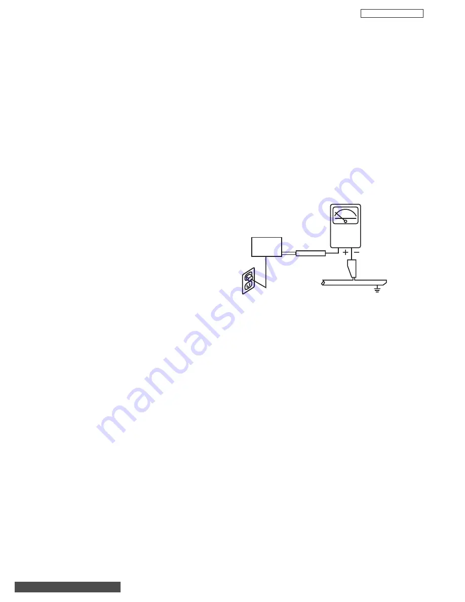
LEAKAGE
CURRENT
TESTER

(READING
SHOULD NOT
BE ABOVE 0.5MIU)

EARTH
GROUND

TEST ALL
EXPOSED
METAL SURFACES

DEVICE
UNDER
TEST

3-WIRE CORD

ALSO TEST WITH PLUG
REVERSED
(USING AC ADAPTER
PLUS AS REQUIRED)

TABLE OF CONTENTS

Summary of Contents for 32HDT50

Page 1: ... PARTS LIST 130 DVI CABLE PIN CONFIGURATION 131 CAUTION These servicing instructions are for use by qualified service personnel only To reduce the risk of electric shock do not perform any servicing other than that contained in the operating instructions unless you are qualified to do so Before servicing this chassis it is important that the service technician read the IMPORTANT SAFETY INSTRUCTION...

Page 2: ...ch is physical ground Using an insulation tester DC500V connect one of its leads to the AC plug jumper and touch with the other lead each exposed metal part antennas screwheads metal overlays control shafts etc particularly any exposed metal part having a return path to the chassis should have a resistor reading over 4MΩ Any resistance value below this range indicates an abnormality which requires...

Page 3: ... panel module will be needed 8 Signal power supply P W B s and PDP driving circuits P W B s are assembled on the rear side of the PDP module take special care with this fragile circuitry particularly Flexible Printed Circuits bonded to surrounding edges of the glass panel They are not strong enough to withstand harsh outer mechanical forces Avoid touching the flexible printed circuits by not only ...

Page 4: ...ment Electrostatically Sensitive ES Devices Some semiconductor solid state devices can be damaged easily by static electricity Such components commonly are called Electrostatically Sensitive ES Devices Examples of typical ES devices are integrated circuits and some field effect transistors and semiconductor chip components The following techniques should be used to help reduce the incidence of com...

Page 5: ...ement IC in the circuit board 2 Carefully bend each IC lead against the circuit foil pad and solder it 3 Clean the soldered areas with a small wire bristle brush It is not necessary to reapply acrylic coating to areas Small signal Discrete Transistor Removal Replacement 1 Remove the defective transistor by clipping its leads as close as possible to the component body 2 Bend into a U shape the end ...

Page 6: ...this technique only on IC connections 1 Carefully remove the damaged copper pattern with a sharp knife Remove only as much copper as absolutely necessary 2 Carefully scratch away the solder resist and acrylic coating if used from the end of the remaining copper pattern 3 Bend a small U in one end of a small gauge jumper wire and carefully crimp it around the IC pin Solder the IC connection 4 Route...

Page 7: ... against the soldering pads with tweezers or with a miniature alligator clip and apply heat to the pad area with a 30 watt iron until solder flows Do not apply heat for more than 3 seconds How to Replace Flat lC Required Tools Soldering iron iron wire or small awl De solder braids Magnifier 1 Remove the solder from all of the pins of a Flat lC by using a de solder braid 2 Put the iron wire under t...

Page 8: ...o an outlet on a circuit different from that to which the receiver is connected Consult the dealer or an experienced radio television technician for help Modifications The FCC requires the user to be notified that any changes or modifications made to this device that are not expressly approved by Hitachi Home Electronics America Inc may void the user s warranty Cables Connections to this device mu...

Page 9: ...of International Business Machines Corporation of the U S A Apple and Macintosh are registered trademarks of Apple Computer Inc VESA is a trademark of a nonprofit organization Video Electronics Standard Association This Class B digital apparatus meets all requirements of the Canadian Interference Causing Equipment Regulations This Class B digital apparatus complies with Canadian ICES 003 Cet appar...

Page 10: ...he monitors The 32 and 42 monitors contain the displaying device which is the plasma display panel module and the driving circuitry which receives the signal from the AVC center and after processing delivers the image to the display module This HITACHI Service Manual is intended for the qualified service personnel and it contains the necessary information for troubleshooting the Plasma television ...

Page 11: ... set set Over 230 cd m2 When RGB is Over 245 cd m2 When RGB is set set All White Pattern Over 50 cd m2 Over 55 cd m2 Contrast Contrast ratio 550 1 typ 600 1 typ Color Color Reproduction Over 16 7 million colors Reproduction Audio Output Audio Output 7w 7w 6Ω 10w 10w 6Ω Panel Main Power Switch PUSH LOCK 1 Switch Operation Sub Power Switch PUSH NON LOCK 1 Switch Input Terminal Video Audio Input 24 p...

Page 12: ... Picture Contrast Brightness Color Tint Sharpness W B Temp Black Enhancement Contrast Mode Color Management Decoding Auto Color Noise Reduction Auto Movie Mode Black Side Panel Settings for Video Signal 23 Contrast Brightness W B Temp Enhancer Input Level Black Side Panel Settings for PC Raster 24 Hor Vert Raster Position Horizontal Clock Clock Phase Adjustment Settings for Sound 25 Vol Balance Ba...

Page 13: ...anel Component Signal Input VIDEO1 VIDEO2 50 2 Input RCA pin 6 Y of VIDEO2 is common input for Composite In Digital Input DVI HDCP 51 1 Input DVI D 24P X1 Selected by component Video1 Digital input priority Audio In L R L ch mono 52 6 Input RCA pin 12 RGB 1 Input Video 5 Input CATVIn 53 1 Input VIDEO2 LINK Video Control Terminal BS 54 No U V Ant Input 55 ANT A IN ANT B IN TO CONV BS IF Input 56 No...

Page 14: ...lass panel has the possibility of being broken or increasing the picture defects At the time of transportation horizontal style is prohibited More over please treat the plasma panel with great care because of a precision apparatus Please instruct transporters so that it should be put into the packing box at the time of shipment There is a possibility that breakage of the panel or defects will incr...

Page 15: ... for professional installer Do not install by yourself ANTENNA Unless your Plasma Television is connected to a cable TV system or to a centralized antenna system a good outdoor color TV antenna is recommended for best performance However if you are located in an exceptionally good signal area that is free from interference and multiple image ghosts an indoor antenna may be sufficient LOCATION Sele...

Page 16: ...so serve as the cursor down and up buttons when in MENU mode VOLUME level Press these buttons to adjust the sound level The volume level will be displayed on the TV screen These buttons also serve as the cursor left and right buttons when in MENU mode 32 DISPLAY MONITOR AUDIO VIDEO CONTROL CENTER 42 DISPLAY MONITOR STANDBY RED ON GREEN MAIN POWER STANDBY RED ON GREEN MAIN POWER PULL POWER MENU SEL...

Page 17: ...5 appears in the top right corner of the TV screen If you have mono sound insert the audio cable into the left audio jack PHONES JACK Use this jack for your head phones The TV s internal speakers can also be heard Turn off the internal speakers see page 46 if you wish to listen to the head phones only LEARNING AV NET Sensor Point your equipment s remote control at this area while using the AV NET ...

Page 18: ...tly to a different source such as a cable box only when ANT B is displayed as a main picture Audio Video Inputs 1 2 3 and 4 The VID1 VID4 buttons will select each video source each time they are pressed Use the audio and video inputs to connect external devices such as VCRs camcorders laserdisc players DVD players etc If you have mono sound insert the audio cable into the left audio jack MONITOR O...

Page 19: ...are as follows DVI Component S Video then composite When using a Set Top Box it is recommended to use a 1080i or 720p input signal To Monitor Connect the Monitor Connection Cable to the AVC center s TO MONITOR connector and to the display monitors FROM AVC connector IR Blaster This jack provides IR output to your external components VCR Cable box DVD player etc With this connection your external c...

Page 20: ...he AV NET button on the remote control Use THUMB STICK or to highlight the component you wish to set up Use THUMB STICK to enter component s SOFT KEY control button The AV Network Setup Wizard will automatically start upon the very first use You can access the Setup Menu Wizard again in the future by pressing the AV net button and then pressing the INFO button NOTES 1 The AVC Center has two IR BLA...

Page 21: ...l Video Input Input 1 Audio Input Using TV Transmission Test POWER PLAY CH UP BACK OK EXIT Move SEL Select Set Input AV Receiver PV Recorder VCR DVD POWER MENU MORE Move INFO Device Setting HITACHI AV NET SET UP DVD Device Code 0 6 7 2 Enter code 9999 to uninstall Video Input Input 1 Audio Input No Connection Transmission Test POWER PLAY CH UP BACK OK EXIT Move SEL Select Set Input HITACHI AV NET ...

Page 22: ...ncepts 0503 Yamaha 0490 0545 0539 Zenith 0591 0503 CABLE BRAND CODE ABC 0003 0008 0014 0017 Americast 0899 Bell Howel 0014 Bell South 0899 Director 0476 General Instrument 0003 0476 0276 0810 GoldStar 0144 Hamlin 0009 0273 Jerrold 0476 0003 0276 0012 0014 0810 Memorex 0000 Motorola 0476 1106 0276 0810 Pace 0237 Panasonic 0107 0000 Philips 0305 0317 Pioneer 0144 0533 0877 1877 Pulsar 0000 Quasar 00...

Page 23: ... R L MONO AUDIO L R S VIDEO VIDEO AUDIO R S VIDEO VIDEO AUDIO R S VIDEO VIDEO MONITOR OUT INPUT 4 INPUT 3 IR BLASTER L MONO L MONO AUDIO Y R L MONO AUDIO INPUT 2 INPUT 1 ANT B TO CONVERTER ANT A DVI HDTV INPUT 1 L AUDIO R AUDIO OUT ANALOG INPUT L MONO R AUDIO RGB TruBass SRS and symbol are trademarks of SRS Labs Inc AC IN TO MONITOR Please use HITACHI specified cable OUTPUT Y PB CB PR CR L R VCR 2...

Page 24: ...oxes Use these connections in place of the standard video connection if your device has this feature Your component outputs may be labeled Y B Y and R Y In this case connect the components B Y output to the TV s PB input and the components R Y output to the TV s PR input Your component outputs may be labeled Y CBCR In this case connect the components CB output to the TV s PB input and the componen...

Page 25: ...rent menu item 3 Press EXIT on the remote control to quickly exit from a menu 4 Press AV NET on the remote control to access the AV Network menu to control external components A V Net EXIT MENU SELECT Locks Chan Manager Aspect Audio Video Move SEL Sel Setup This part of the screen shows which selections are available This part of the screen shows which Remote Control buttons to use ...

Page 26: ...dio Source Select between three Audio Sources Internal Speakers Select internal or external speakers Auto Noise Cancel Eliminates the noise between stations Perfect Volume Adjust volume in fixed setting Mode Choose the picture format aspect ratio Ant A View edit Channel ID Scan and Lock settings in antenna A Ant B View edit Channel ID Scan and Lock settings in antenna B Change Access Code Change L...

Page 27: ...Press MENU on the remote control to display the different features in RGB MODE 3 Press the THUMB STICK buttons to highlight a different feature 4 Press EXIT on the remote control to quickly exit from a menu TV RGB EXIT MENU SELECT Setup Aspect Video Move SEL Sel This part of the screen shows which Remote Control buttons to use ...

Page 28: ...al Aspect in 4 3 standard Full Aspect in 16 9 standard Auto Adjust Automatically adjust the geometry to fit the screen Horizontal Position Adjust horizontal position Vertical Position Adjust vertical position Horizontal Clock Adjusts the dot clock frequency to reduce the vertical stripe Clock Phase Adjusts the phase to correct blurred or unstable images Reset Recall the factory preset data of the ...

Page 29: ... Adjustment 31 3 3 Brightness Check 31 4 Vs Va Voltage Adjustment 32 5 White balance adjustment 33 5 1 Video Color Temperature Adjustment High 33 5 2 Video Color Temperature Adjustment Medium 33 5 3 Video Color Temperature Adjustment Standard 34 5 4 Video Color Temperature Adjustment Black and White 34 5 5 PC Color Temperature Adjustment High 34 5 6 Color Temperature Setting Correction 34 5 7 Whit...

Page 30: ...ed for changing data values MENU key is used to advance through the adjustment mode menus and pages ADJUST MODE XXXX RGB 480P FACT RESET V POSITION FIRMWARE VERSION BACK TO ADJUSTMENTS EXIT MENU SELECT B To make a selection use the CURSOR keys on the AVC front control panel or the Remote Control C After finishing the necessary adjustment press the R C EXIT key or EXIT key on the front panel Adjust...

Page 31: ...t unplug from AC outlet until this operation is completed and do not perform any key operation either After this operation each factory setting and adjust mode data should reset to delivery setting automatically 3 3 BRIGHTNESS CHECK Preparation 1 Start checking 20 minutes or more after the power is turned ON 2 Receive the color bar signal 3 The vertical incident illumination on the screen should b...

Page 32: ... 1V of the value specified in the label on the panel 1 2 Turn VaADJ VR51 to adjust Vs voltage to be within 0 2V of the value specified in the label on the panel 1 3 Reconfirm that Vs voltage remains within 0 1V of the value Readjust if Itís outside the margin Label example 2 Label position Reference Remarks 1 Permissive level of voltage in case sufficient time of heat run performed Vs within 0 45V...

Page 33: ...p down the two or one among Adjustment R G B DRIVE HIGH and adjust the value shown in the following At least one of the data should be FF Specification Video Color temperature HIGH x 0 285 0 005 y 0 298 0 005 Color temp 9200K Remarks 1 Color temperature should be adjusted under the condition in which the screen is the brightest thus the initial value for adjustment is set to its maximum 2 Adjustme...

Page 34: ...t should be done after video color temperature adjustment 2 Confirm that it s set as factory adjustment mode 3 Input WINDOW signal window ratio 6 25 into RGB terminals at VGA 60 0 7V No set up 4 Set AVC to shipment 5 Confirm that the screen size is FULL Adjustment 1 Perform the following adjustment with the remote control 2 Set the CRT color analyzer CA 100 at the center of the panel 3 Ensure that...

Page 35: ...35 PT3 E G AVC3 U 5 7 WHITE BALANCE ADJUSTMENT OSD FLOW DIAGRAM BACK TO ADJUSTMENTS ...

Page 36: ...he symmetry of the pattern top bottom 4 Check the vertical position and the balance top bottom Remarks 1 RGB XGA 60Hz 3 SCREEN 0 1 2 2 1 0 A B 7 FACTORY RESET After all of the adjustments of main chassis are finished perform FACTORY RESET 1 Enter Adjustment Mode by the method described in sub items 1 1 and 1 2 from page 30 Adjustment Procedure Start up 2 From the first menu in Adjustment Mode sele...

Page 37: ...c Picture Mode Day Color Management Off Magenta 71 Red 70 Yellow 50 Green 50 Cyan 40 Blue 76 Color Decoding RGB Red 50 Green 50 Color 50 Picture Mode Day Tint 50 Picture Mode Day Auto Color Off Picture Mode Day Noise Reduction Low Picture Mode Day Auto Movie Mode Off Picture Mode Day Audio Treble 50 Bass 65 Balance 50 SRS Trubass Medium Matrix Surround Off Audio Source Stereo Mono SAP Stereo Inter...

Page 38: ...red Set The Inputs Input 1 Rename Not Registered Input 2 Rename Not Registered Auto Link Auto Remote Off Off Input 3 Rename Not Registered Input 4 Rename Not Registered Input 5 Rename Not Registered Video Power Save On Color System YPBPR1 Auto On Input Signal YPBPR2 Auto On Input Signal Black Side Panel Off Set Event Timer Event1 2 3 4 Not Registered Set Closed Caption Caption Display Auto Mode Ca...

Page 39: ...M STD B DRIVE Blue Drive Gain Control B W FF HIGH MEDIUM R CUTOFF Red Cutoff Control STD 3E HIGH MEDIUM G CUTOFF Green Cutoff Control STD 3E B W HIGH B CUTOFF Blue Cutoff Control MEDIUM 3E UPD64083 3D Y C B9H Read Mode SYNCDET Sync Detection 0 Sync 1 No Sync 01 F STD Frame Sync Nonstandard Detection 0 Standard 1 Non standard 01 V STD Vertical Sync Nonstandard Detection 0 Standard 1 Non standard 01...

Page 40: ...HC1 NR TV NR High 03 02 YHC3 NTSC NR High 03 00 YHC3 NR 32 37 42 Y Output High Frequency Coring NTSC NR High 03 02 HC1 TV NR High 03 00 HC1 NR TV NR High 03 02 HC3 NTSC NR High 03 00 HC3 NR 50 Y Output High Frequency Coring NTSC NR High 03 02 TA1383F Main Read Mode D9H HSYNC M Main H Sync Signal FF VSYNC M Main V Sync Signal 7F CSYNC M Main C Sync Signal 01 TA1383F SUB Read Mode HSYNC S Sub H Sync...

Page 41: ...0i FE 00 STOFF00 Main NTSC TOF Center Frequency Switch 0 OFF 1 MIN 0 8 fsc 7 MAX 1 5 fsc TV NTSC 07 00 STOFQ 0 Main NTSC TOF Q Characteristic Switch 0 MIN 0 6 7 MAX 1 2 TV NTSC 07 00 TA1383F MAIN SUB D8H DAH Y DL1 4 TV NTSC 03 01 Y DL1 D Y Delay Time Adjust 1 Base Band Section 0 10 ns 1 0 ns 2 10 ns 3 20 ns 480i 480p 720p 1080i By pass YPBPR DVI 03 00 Y DL2 0 Y Delay Time Adjust 2 NTSC Section 0 O...

Page 42: ...ync Mode Switch 0 Normal PLL Mode 1 Sync Output Mode 480i 01 00 48ISEP4 480i Separator Mode Switch 0 ON 1 OFF TV NTSC 01 00 B WM TV NTSC 480i 03 02 B WM NR TV NTSC 480i NR 03 01 B WN 480p 720p 1080i 03 00 B WN NR 32 37 42 Band Width Filter Switch 0 OFF 1 11 3MHz 3dB 2 16MHz 3dB 3 Mute 480p 720p 1080i NR 03 02 BWM TV NTSC 480i 03 02 BWM NR TV NTSC 480i NR 03 01 BWN 480p 720p 1080i 03 00 BWN NR 50 B...

Page 43: ...PC Control 32 01 00 APC3742 APC Control 37 42 01 00 PDP VER PDP Microcomputer Version Display 03E7 PDP TM PDP Panel Drive Time FFFF CCFMD D TV VID 01 00 CCFMD H Brightness Gradation Priority Switch PC 01 00 CCFORMF NTSC EBU Switch SDTV 01 00 CCFORMG HDTV 01 00 CCFORMH PC 01 00 DCBONH TV VID Col Temp High 01 00 DCBONML TV VID Col Temp Med Std BW 01 01 DCBON H Tracking Adjustment Switch PC 01 01 WBC...

Page 44: ...HP L TV 1F 1F HPL NR TV NR 1F 0D HP 3 NTSC 1F 14 HP 5 480i 1F 14 HP3 NR NTSC NR 1F 0B HP5 NR 480i NR 1F 0B HP 6 480p 1F 0E HP 7 720p 1F 0B HP 8 1080i 1F 0B HPN NR 50 Sharpness 480p 720p 1080i NR 1F 06 H EL TV 03 00 H EL NR TV 03 00 H E3 NTSC 03 01 H E5 480i 03 00 H E3 NR NTSC NR 03 00 H E5 NR 480i NR 03 00 H EB 720p 1080i 03 03 H E6 480P 03 03 H EN NR 32 37 42 Horizontal Enhance Gain 0_3 Gain 480p...

Page 45: ...R LV3 NTSC 07 04 CNR LV5 480i 07 01 CNR LV6 480p 07 01 CNR LVB CNR Input Level 0 OFF 1_7 Input Gain 720p 1080i 07 01 V POSI7 720p 7E 3F V POSI8 TV Vertical Position 0 63_63 0_126 63 1080i 7E 3F BLK LV4 TV NTSC FE 7F BLK LVD 480i 480p 720p 1080i Bypass FE 7F BLK LVH Brightness Amp 0 127_127 0_254 127 PC FE 7F RGBAMPD TV Video FE 7F RGBAMPH Contrast Amp 0 127_127 0_254 127 PC FE 7F BRTCEN4 TV NTSC M...

Page 46: ...C4 ORG FC4 Adjustment MENU _ _ ETC POWSAVE PC Power Save 0 OFF 1 ON 01 01 POWS TM PC Power Save Timer second FE 0F INPUT1 Main YPbPr freq detection fixed mode 04 00 INPUT2 Sub YPbPr freq detection fixed mode 04 00 S CSTEP Sub Contrast adjustment step FE 06 S C UP Sub Contrast adjustment maximum limit FE E6 S C LOW Sub Contrast adjustment minimum limit FE E0 M MAX Main maximum luminosity display FE...

Page 47: ...1080i FE 00 BBLACKQ DVI 480i 480p FE 00 BBLACKS 32 37 42 CB PB Black Level Control 00 OFF 01 MIN_FE MAX DVI 720p 1080i FE 00 RBLACKQ DVI 480i 480p FE 00 RBLACKS 32 37 42 CR PR Black Level Control 00 OFF 01 MIN_FE MAX DVI 720p 1080i FE 00 BBLCKQ DVI 480i 480p FE 00 BBLCKS 50 CB PB Black Level Control 00 OFF 01 MIN_FE MAX DVI 720p 1080i FE 00 RBLCKQ DVI 480i 480p FE 00 RBLCKS 50 CR PR Black Level Co...

Page 48: ...shock and second damage Check D901 D902 C901 C907 etc Is R915 open Trouble of Main Switching regulator Page 49 Check I901 D911 T901 C913 C918 etc Check H901 C909 etc Protection circuit Operation Page 50 Is Q933 G voltage over 1 0V Yes Yes Yes No Yes No No No A B Has F902 blown Has F901 blown Check AVC AV PWB I001 Q227 Q228 etc Note 1 Disconnect the MONITOR connection cables DVI DIN and press Sub P...

Page 49: ...n voltage at the moment of power ON below 16V Check Q930 Q931 etc Yes Check Q934 D936 D938 I902 D909 etc No A Is Q930 C voltage over 3 5V Check C910 D938 T901 I901 I902 etc Yes No Check D903 D906 etc Yes No Check D905 C912 etc Yes No Is I901 4 regular voltage below 10V TROUBLESHOOTING FLOWCHARTS 2 OF 4 ...

Page 50: ...tage below 3 8V Check D934 I930 I931 I933 etc Yes No Is D939 A voltage below 3 8V Check D935 etc Or check AV PWB Yes No Is D947 K voltage above 5 7V Check I931 D950 etc Yes No Is D948 K voltage above 6 6V Check I933 D949 etc Yes No Is D955 K voltage above 9 5V Check I930 D959 etc Yes No Check Q933 etc TROUBLESHOOTING FLOWCHARTS 3 OF 4 ...

Page 51: ...ower Supply Unit Yes No C Check SIGNAL AUDIO PWB I001 Q005 Q006 etc Yes Is the power indicator LED color red even though it s powered ON by remote controller or AVC front switch with cable connection to AVC No Presume the wrong PWB by Self Diagnostic function TROUBLESHOOTING FLOWCHARTS 4 OF 4 ...

Page 52: ...n 5 seconds 2 Make sure Power Cord of AC line is connected to the PDP Monitor 3 If PDP Monitor has no failure it enters Burn in mode 4 Turning off the Main Power switch would cancel the Self Diagnosis mode 5 The next table shows the PDP PWB in which failure most probably would be allocated according to the number of blinks Blinking condition of power indication light ex 2 blinks Number of red blin...

Page 53: ... I001 PIN 31 I001 PIN 23 I001 PIN 25 I001 PIN 62 I001 PIN 64 I001 PIN 56 I001 PIN 53 I001 PIN 52 I001 PIN 55 1 2 3 4 5 6 7 8 9 10 11 12 WAVEFORMS AT EACH SECTION Numbers inside circle correspond to locations shown in the circuit diagram TABLE OF CONTENTS ...

Page 54: ...0FP PIN 20 TP305 P50FP PIN 19 TP306 P50FP PIN 17 TP307 P50FP PIN 16 TP308 P50FP PIN 15 TP309 P50FP PIN 13 TP310 P50FP PIN 12 U102 PIN 18 U101 PIN 18 22 23 24 19 20 21 16 17 18 13 14 15 WAVEFORMS AT EACH SECTION Numbers inside circle correspond to locations shown in the circuit diagram ...

Page 55: ...6 TPX55 IX01 PIN 58 TPW03 IW01 PIN 84 after LPF TPZ23 IW01 PIN 83 after chroma I001 PIN 54 I001 PIN 55 I001 PIN 59 I001 PIN 58 31 32 33 28 29 30 25 26 27 WAVEFORMS AT EACH SECTION Numbers inside circle correspond to locations shown in the circuit diagram ...

Page 56: ... 69 0 00 7 0 00 19 0 00 20 0 00 70 0 00 I004 8 0 00 20 0 00 21 0 00 71 0 00 9 5 11 21 0 00 22 0 00 72 0 00 10 5 11 22 0 00 23 2 83 73 3 18 11 5 11 I202 23 0 00 24 0 00 74 3 18 12 0 00 24 3 29 25 2 84 75 3 24 13 0 00 25 0 00 26 1 58 76 3 79 14 0 00 26 0 00 27 0 00 77 3 72 15 0 00 27 0 00 28 5 11 78 3 28 16 5 11 28 0 00 29 5 11 79 3 26 1 3 68 29 0 00 30 5 11 80 0 00 2 5 24 30 3 29 31 5 11 81 3 27 3 ...

Page 57: ... 6 3 29 E 0 00 Q236 B 0 70 3 5 09 7 0 00 Q211 B 0 70 C 0 00 4 5 09 8 3 29 C 0 00 Symbol pin No DC Voltage 5 5 09 Symbol pin No DC Voltage E 0 00 E 0 00 I204 6 0 00 E 0 00 Q212 B 0 33 Q241 B 0 10 7 0 00 Q001 B 0 00 C 1 57 C 3 44 8 0 00 C 0 46 E 0 00 E 0 00 9 5 09 E 0 00 Q313 B 0 00 Q242 B 0 10 10 5 09 Q002 B 0 00 C 3 28 C 3 43 11 5 09 C 5 11 E 0 00 E 0 00 12 5 11 E 0 00 Q214 B 0 00 Q246 B 0 00 13 5...

Page 58: ...22 E 0 00 13 4 43 8 4 99 C 8 99 Q409A B 0 00 14 0 00 1 5 65 E 3 77 C 0 00 15 4 49 2 4 90 Q406A B 4 22 E 3 97 16 8 99 I906 3 5 65 C 8 99 Q411 B 4 53 1 4 49 4 3 92 E 0 00 C 8 39 2 1 37 5 0 00 Q407 B 0 00 E 3 95 3 4 53 6 0 00 C 0 00 Q411A B 4 53 4 8 99 7 4 97 C 8 38 I402 5 4 50 8 4 97 E 8 99 6 0 00 1 3 93 Q412 B 8 39 7 3 48 I907 2 9 83 C 4 79 8 4 53 3 0 00 E 8 99 9 5 48 4 9 00 Q412A B 8 39 10 4 49 5 ...

Page 59: ... 0 20 13 3 29 5 0 00 QJA4 B 0 00 14 3 29 6 0 00 C 0 00 15 3 29 7 4 99 E 0 20 16 0 00 8 4 99 QJA8 B 0 00 17 3 29 1 4 99 C 0 00 18 0 00 2 4 40 E 0 00 19 0 00 3 4 99 QJC2 B 0 00 20 3 29 IJ06 4 4 99 C 0 20 21 0 00 5 0 00 22 3 29 6 0 00 23 0 00 7 3 30 24 3 29 8 3 30 25 0 00 E 0 65 26 0 00 QJ01 B 0 00 27 3 29 C 0 00 28 0 00 E 0 65 29 0 00 QJ05 B 0 00 30 3 29 C 0 00 31 0 00 E 0 65 32 3 29 QJ09 B 0 00 33 ...

Page 60: ...8 3 89 IX02 2 0 50 60 0 00 C 0 00 9 4 40 3 0 69 61 4 85 E 3 86 10 3 89 4 8 82 62 0 00 QX03 B 4 53 11 4 40 5 4 87 63 4 85 C 8 89 12 4 36 6 0 00 64 4 95 E 2 97 13 0 10 7 4 60 1 2 90 QX04 B 3 63 14 4 85 8 0 00 2 0 00 C 8 89 IX01 15 3 88 9 4 63 3 2 08 E 3 68 16 4 40 10 4 60 4 0 00 QX05 B 4 34 17 3 88 11 0 80 5 2 08 C 8 89 18 4 40 12 0 60 IX03 6 0 97 E 0 00 19 4 36 13 0 79 7 0 00 QX08 B 0 42 20 0 10 14...

Page 61: ... 00 QX22 B 1 70 3 2 08 C 0 00 4 0 00 E 2 32 5 2 08 QX23 B 1 69 IX04 6 1 44 C 0 00 7 0 00 E 2 35 8 2 20 QX24 B 1 72 9 1 80 C 0 00 10 0 00 E 2 35 11 2 84 QX25 B 1 72 12 0 00 C 0 00 13 4 89 E 2 33 14 2 90 QX26 B 1 70 15 0 00 C 0 00 16 2 84 E 3 61 QX30 B 4 22 C 8 82 E 3 66 QX31 B 4 28 C 8 82 E 2 37 QX37 B 1 77 C 0 00 E 4 25 QX38 B 3 67 C 0 00 ...

Page 62: ...2 3 22 20 0 00 78 0 00 1 8 89 13 8 77 21 0 00 79 0 00 2 2 51 14 5 18 22 0 00 80 0 00 3 4 12 15 0 00 23 0 00 81 2 41 4 1 95 16 5 24 24 0 00 82 1 02 5 0 00 25 0 00 83 1 44 6 2 35 26 0 00 84 1 44 7 0 00 27 0 00 85 1 02 8 4 66 28 0 00 86 0 00 9 6 19 29 0 00 87 0 00 10 5 02 30 0 00 88 1 08 11 0 00 31 2 43 89 0 64 12 0 00 32 2 43 90 0 74 13 4 80 33 0 00 91 1 21 14 4 89 34 0 00 92 2 41 15 0 00 35 0 00 93...

Page 63: ...6 2 92 C 8 34 E 0 00 E 3 81 E 8 96 QZ07 B 0 00 QZ38 B 4 44 QW11 B 8 34 C 6 02 C 8 77 C 2 79 E 3 52 1 8 16 E 2 17 QZ11 B 2 90 2 8 16 QW12 B 2 79 C 0 00 QZ39 3 8 78 C 8 96 E 3 51 4 3 92 E 8 97 QZ12 B 2 90 5 3 47 QW13 B 8 35 C 0 00 6 2 92 C 6 33 E 3 61 E 3 81 QZ13 B 4 25 QZ40 B 4 44 C 8 90 C 8 78 E 3 75 E 0 67 QZ14 B 3 93 QZ41 B 0 00 C 8 90 C 0 00 E 5 35 E 0 67 QZ15 B 5 99 QZ42 B 0 00 C 8 90 C 0 00 E...

Page 64: ... QZ39 3 8 78 C 8 96 9 0 00 E 3 51 4 3 92 E 8 97 10 17 34 QZ12 B 2 90 5 3 47 QW13 B 8 35 11 17 34 C 0 00 6 2 92 C 6 33 12 15 28 E 3 61 E 3 81 E 13 0 00 QZ13 B 4 25 QZ40 B 4 44 QW14 B 14 0 88 C 8 90 C 8 78 C 15 1 00 E 3 75 E 0 67 E 8 97 16 0 00 QZ14 B 3 93 QZ41 B 0 00 QW15 B 8 35 1 0 00 C 8 90 C 0 00 C 6 35 2 5 64 E 5 35 E 0 67 I931 3 3 45 QZ15 B 5 99 QZ42 B 0 00 4 1 76 C 8 90 C 0 00 5 17 36 E 0 00 ...

Page 65: ...6 3 3 16 1 5 17 0 0 57 0 0 17 0 17 0 0 18 0 0 58 5 2 18 3 3 18 1 9 19 0 0 59 5 2 19 0 19 1 6 20 0 0 60 5 2 20 3 3 20 0 0 21 0 0 61 5 2 21 0 0 22 0 0 62 5 2 22 1 5 23 0 0 63 0 0 Symbol Pin No DC Voltage 23 1 4 24 3 3 64 5 2 1 0 0 24 1 6 25 0 7 65 3 3 I002 2 0 0 25 1 6 26 3 3 66 5 1 3 0 0 26 3 3 27 0 0 67 5 0 4 0 0 27 3 2 28 0 1 68 5 1 5 5 2 28 3 3 29 5 2 69 5 1 6 5 2 29 0 0 30 5 2 70 0 0 7 0 0 30 2...

Page 66: ... I600 34 1 3 10 1 6 35 1 1 11 1 6 36 1 6 12 1 6 37 1 3 I600 13 1 6 38 3 2 14 1 3 39 0 0 15 1 5 40 0 0 16 1 4 41 3 4 17 1 9 42 0 0 18 3 3 43 3 3 19 0 0 44 1 7 20 1 6 45 0 0 21 1 3 46 2 4 22 1 3 47 3 3 23 1 2 48 3 3 24 1 2 49 0 0 25 1 2 50 0 0 51 0 0 52 0 0 53 0 0 54 0 0 55 0 0 56 0 0 57 3 3 58 0 0 59 0 0 60 0 0 61 0 0 62 0 0 63 0 0 64 0 0 65 0 0 66 0 0 67 3 2 68 0 0 69 0 0 70 0 0 71 0 0 72 0 0 73 0...

Page 67: ...3 0 16 12 0 1 6 1 32 6 8 92 0 0 17 0 0 2 6 1 B 0 9 93 3 0 18 4 9 3 6 1 Q001 C 0 1 94 3 0 19 5 3 IC403 4 6 1 E 0 0 95 3 2 20 5 5 5 6 1 B 4 4 96 3 1 21 1 8 6 0 0 Q005 C 5 0 97 3 3 22 6 0 7 0 0 E 5 1 98 0 0 23 6 0 8 0 0 B 5 1 99 0 0 24 6 0 9 4 9 Q006 C 0 1 100 3 3 25 6 0 10 0 0 E 5 1 1 7 2 26 6 0 11 0 1 S 0 7 2 9 9 27 6 0 12 0 1 Q201 D 0 0 3 2 6 28 0 0 13 4 2 G 0 0 I602 4 5 0 29 0 0 14 0 1 S 0 0 5 4 ...

Page 68: ...E 0 0 B 1 3 Q402 C 0 7 E 0 7 B 0 0 Q403 C 0 0 E 0 0 B 0 0 Q404 C 0 0 E 0 0 B 0 0 Q405 C 0 0 E 0 0 B 5 0 Q406 C 0 0 E 0 0 B 0 1 Q407 C 0 0 E 0 0 B 0 0 Q408 C 1 3 E 0 0 B 0 7 Q501 C 0 1 E 0 0 B 9 9 Q504 C 0 0 E 0 0 S 3 3 Q600 D 5 0 G 3 4 S 3 3 Q601 D 5 0 G 3 4 1 0 0 2 0 1 Q602 3 0 1 4 0 0 5 0 7 6 3 9 ...

Page 69: ...arts is subject to be altered for improvement AVC3 U Control PRODUCT SAFETY NOTE Components marked with a and shaded have special characteristics important to safety Before replacing any of these components read carefully the PRODUCT SAFETY NOTICE of this Service Manual Don t degrade the safety of the receiver through improper servicing BASIC CIRCUIT DIAGRAM PT3 E G AVC3 U Control 69 BACK TO TABLE...

Page 70: ...s is a basic circuit diagram the value of the parts is subject to be altered for improvement AVC3 U MPU PRODUCT SAFETY NOTE Components marked with a and shaded have special characteristics important to safety Before replacing any of these components read carefully the PRODUCT SAFETY NOTICE of this Service Manual Don t degrade the safety of the receiver through improper servicing BASIC CIRCUIT DIAG...

Page 71: ...lue of the parts is subject to be altered for improvement AVC3 U Tuner Audio PRODUCT SAFETY NOTE Components marked with a and shaded have special characteristics important to safety Before replacing any of these components read carefully the PRODUCT SAFETY NOTICE of this Service Manual Don t degrade the safety of the receiver through improper servicing BASIC CIRCUIT DIAGRAM PT3 E G AVC3 U Tuner Au...

Page 72: ...m the value of the parts is subject to be altered for improvement AVC3 U Input PRODUCT SAFETY NOTE Components marked with a and shaded have special characteristics important to safety Before replacing any of these components read carefully the PRODUCT SAFETY NOTICE of this Service Manual Don t degrade the safety of the receiver through improper servicing BASIC CIRCUIT DIAGRAM PT3 E G AVC3 U Input ...

Page 73: ...the value of the parts is subject to be altered for improvement AVC3 U Video PRODUCT SAFETY NOTE Components marked with a and shaded have special characteristics important to safety Before replacing any of these components read carefully the PRODUCT SAFETY NOTICE of this Service Manual Don t degrade the safety of the receiver through improper servicing BASIC CIRCUIT DIAGRAM PT3 E G AVC3 U Video 73...

Page 74: ...ith a and shaded have special characteristics important to safety Before replacing any of these components read carefully the PRODUCT SAFETY NOTICE of this Service Manual Don t degrade the safety of the receiver through improper servicing BASIC CIRCUIT DIAGRAM PT3 E G AVC3 U Power 74 1 2 3 4 5 6 A B C D E For MPU For TUNER AUDIO For TUNER AUDIO For INPUT For VIDEO For TUNER AUDIO A For TUNER AUDIO...

Page 75: ...he value of the parts is subject to be altered for improvement AVC3 U DVI PRODUCT SAFETY NOTE Components marked with a and shaded have special characteristics important to safety Before replacing any of these components read carefully the PRODUCT SAFETY NOTICE of this Service Manual Don t degrade the safety of the receiver through improper servicing BASIC CIRCUIT DIAGRAM PT3 E G AVC3 U DVI 75 ...

Page 76: ...alue of the parts is subject to be altered for improvement AVC3 U Power 1 2 PRODUCT SAFETY NOTE Components marked with a and shaded have special characteristics important to safety Before replacing any of these components read carefully the PRODUCT SAFETY NOTICE of this Service Manual Don t degrade the safety of the receiver through improper servicing BASIC CIRCUIT DIAGRAM PT3 E G AVC3 U Power 76 ...

Page 77: ...alue of the parts is subject to be altered for improvement AVC3 U Power 2 2 PRODUCT SAFETY NOTE Components marked with a and shaded have special characteristics important to safety Before replacing any of these components read carefully the PRODUCT SAFETY NOTICE of this Service Manual Don t degrade the safety of the receiver through improper servicing BASIC CIRCUIT DIAGRAM PT3 E G AVC3 U Power 77 ...

Page 78: ...value of the parts is subject to be altered for improvement AVC3 U AV Jig PRODUCT SAFETY NOTE Components marked with a and shaded have special characteristics important to safety Before replacing any of these components read carefully the PRODUCT SAFETY NOTICE of this Service Manual Don t degrade the safety of the receiver through improper servicing BASIC CIRCUIT DIAGRAM PT3 E G AVC3 U AV Jig 78 ...

Page 79: ...value of the parts is subject to be altered for improvement PT3 E G Filter PRODUCT SAFETY NOTE Components marked with a and shaded have special characteristics important to safety Before replacing any of these components read carefully the PRODUCT SAFETY NOTICE of this Service Manual Don t degrade the safety of the receiver through improper servicing BASIC CIRCUIT DIAGRAM PT3 E G AVC3 U Filter 79 ...

Page 80: ...red for improvement PT3 E G Signal Audio 1 PRODUCT SAFETY NOTE Components marked with a and shaded have special characteristics important to safety Before replacing any of these components read carefully the PRODUCT SAFETY NOTICE of this Service Manual Don t degrade the safety of the receiver through improper servicing BASIC CIRCUIT DIAGRAM PT3 E G AVC3 U Signal Audio 1 80 For SIGNAL AUDIO 2 For S...

Page 81: ...r improvement PT3 E G Signal Audio 2 PRODUCT SAFETY NOTE Components marked with a and shaded have special characteristics important to safety Before replacing any of these components read carefully the PRODUCT SAFETY NOTICE of this Service Manual Don t degrade the safety of the receiver through improper servicing BASIC CIRCUIT DIAGRAM PT3 E G AVC3 U Signal Audio 2 81 For SIGNAL AUDIO 1 For SIGNAL ...

Page 82: ...r improvement PT3 E G Signal Audio 3 PRODUCT SAFETY NOTE Components marked with a and shaded have special characteristics important to safety Before replacing any of these components read carefully the PRODUCT SAFETY NOTICE of this Service Manual Don t degrade the safety of the receiver through improper servicing BASIC CIRCUIT DIAGRAM PT3 E G AVC3 U Signal Audio 3 82 For SIGNAL AUDIO 1 For SIGNAL ...

Page 83: ... G Signal Audio 4 PRODUCT SAFETY NOTE Components marked with a and shaded have special characteristics important to safety Before replacing any of these components read carefully the PRODUCT SAFETY NOTICE of this Service Manual Don t degrade the safety of the receiver through improper servicing BASIC CIRCUIT DIAGRAM PT3 E G AVC3 U Signal Audio 4 83 For SIGNAL AUDIO 1 For SIGNAL AUDIO 2 For SIGNAL ...

Page 84: ...PRINTED CIRCUIT BOARD AVC3 U Audio Video PWB 84 PT3 E G AVC3 U BACK TO TABLE OF CONTENTS ...

Page 85: ...PRINTED CIRCUIT BOARD AVC3 U Audio Video PWB 85 PT3 E G AVC3 U ...

Page 86: ...PRINTED CIRCUIT BOARD AVC3 U Power PWB 86 PT3 E G AVC3 U ...

Page 87: ...PRINTED CIRCUIT BOARD AVC3 U Power PWB 87 PT3 E G AVC3 U ...

Page 88: ...PRINTED CIRCUIT BOARD AVC3 U SW Jig Control Filter PWB 88 PT3 E G AVC3 U PT3 E G FILTER PWB ...

Page 89: ...PT3 E G AVC3 U PRINTED CIRCUIT BOARD PT3 E G Signal Audio PWB 89 ...

Page 90: ...PRINTED CIRCUIT BOARD PT3 E G Signal Audio PWB 90 PT3 E G AVC3 U ...

Page 91: ...D IN IR DET SUB CCD SEL MAIN CCD SEL AC IN OSD VSYNC IN OSD HSYNC IN AUDIO SEL2 HPVOL A AGC A MUTE1 A MUTE2 POWER1 POWER2 _POWER1 FSTB 5V FA 5 5V D 1 8V D 3 3V AVDET 5 5 V STB 3 3V STB 5V 120V POWER2 POWER1 AV_PWB IR IN2 QX13 Y V QX14 _C Q223 224 S VIDEO Q218 219 M VIDEO PS PS IR TXD PDP IR RXD PDP IR TXD RXD P I204 BU4053BCF 5V I203 3 3V 5V Buffer I908 SI 3090KM I907 SI 3090KM 3 3V _POWER1 I906 S...

Page 92: ...PT3 E G AVC3 U BLOCK DIAGRAM FC4 Unit 92 ...

Page 93: ...3 D947 5 7V POWER1 AVC3 U POWER P W B Detect Voltage down D948 6 6V Detect Voltage over D955 9 5V D944 2 8V D942 3 8V D941 3 8V SW Q932 DC DC converter Photo coupler I905 AC Clock T901 Switching regulator I901 Photo coupler I902 Error Amp Q934 D938 FC4 IJ05 Reg SI 3033LSA IJ06 Reg SI 3050LSA I906 Reg SI 3050LSA I905 Reg SI 3050LSA STB 3 3V Reg SI 3033LSA I910 FE 30V FE 5V V 5V DVI 5V DVI 3 3V I908...

Page 94: ... AUDIO OUT TRUBASS RXD0 TXD0 AVDET PDP GO CPU GO IRQ MUT E SPRL Y SDA1 SCL1 FVPP MD1 RES RLED GLED REM L R PDP Microcomputer From AVC LVDS TRANSMITTER PDLVD S STB 5V SUBSW LEVEL CONVERT PROGRAM Writing 16MHz MPU CONTROL BLOCK DIAGRAM Plasma Monitor ...

Page 95: ... CONT MUTE CONT SCL1 SDA1 Lch IN Rch IN NJW1133A MASTER VOL BALANCE TONE CONT SURR ON OFF NJM2192AM TRUBASS MUTE RELAY TA2020 020 DIGITAL POWER AMP 12V BU4052 TRUBASS POWER OFF DET MUTE DRIVE RELAY DRIVE SUB WOOFER OUT PM ON RELAY MUTE MUTE AUDIIO CIRCUIT BLOCK DIAGRAM Plasma Monitor ...

Page 96: ...sing unit Y PWB X PWB X Sustain Circuit Y Sustain Circuit PDP Panel Unit Address Driver Scan Driver Driver Controller LVDS Receiver Signal Controller Data Controller Logic Control unit TMDS Receiver RGBHV Audio Signal Scan Driver LED PWB Sensor Window Digital Audio Amplifier Filter unit Sub Woofer Output LVDS Transmitter Power Unit AVC I F Signal Power Audio Power Connector 2 Systems PDP Panel Mod...

Page 97: ...o PDP 4 6 Vcc 5 1V Vcc 6 6 NC HALFTONE YM NC HALFTONE YM 45 5 Audio L Audio L 5 5 GND GND 46 6 Audio R Audio R 6 PPA CNPPA 4 L L 47 7 PDDET PDDET 7 1 A 12V 13V 1 3 GND GND 48 8 AVDET2 AVDET2 8 2 A 12V 13V 2 CN64 CN23 2 R R 49 3 A GND GND 3 1 Va 60V Va 1 1 GND GND 50 4 A GND GND 4 2 NC NC 2 3 Vcc Vcc 3 4 GND GND 4 5 GND GND 5 Xsus PFSH 6 GND GND 6 1 GND 7 NC NC 7 2 RXD 8 Vs 80V Vs 8 3 BUSY 9 Vs 80V...

Page 98: ... 5 1V Vcc 6 6 NC HALFTONE YM NC HALFTONE YM 45 5 Audio L Audio L 5 5 GND GND 46 6 Audio R Audio R 6 PPA CNPPA 4 L L 47 7 PDDET PDDET 7 1 A 12V 13V 1 3 GND GND 48 8 AVDET2 AVDET2 8 2 A 12V 13V 2 CN64 CN23 2 R R 49 3 A GND GND 3 1 Va 60V Va 1 1 GND GND 50 4 A GND GND 4 2 NC NC 2 3 Vcc Vcc 3 4 GND GND 4 5 GND GND 5 Xsus PFSH 6 GND GND 6 1 GND 7 NC NC 7 2 RXD 8 Vs 80V Vs 8 3 BUSY 9 Vs 80V Vs 9 4 VPP 1...

Page 99: ...PT3 E G AVC3 U AVC3 U CHASSIS WIRING DRAWING 99 BACK TO TABLE OF CONTENTS ...

Page 100: ...100 PT3 E G AVC3 U PT3 E G CHASSIS WIRING DRAWING 42 Plasma Monitor Front ...

Page 101: ...101 PT3 E G AVC3 U PT3 E G CHASSIS WIRING DRAWING 42 Plasma Monitor Back ...

Page 102: ...102 PT3 E G AVC3 U PT3 E G CHASSIS WIRING DRAWING 32 Plasma Monitor Front ...

Page 103: ...103 PT3 E G AVC3 U PT3 E G CHASSIS WIRING DRAWING 32 Plasma Monitor Back ...

Page 104: ...092 AVC30 TERMINAL METAL PM25801 3 PIECES M3 10 T NE 4525404 6 HCP131 ASSEMBLY CS00721 AV PWB ASSEMBLY POWER PWB ASSEMBLY CONTROL PWB ASSEMBLY JP06471 JT23981 HP00771 UL CSA POWER CORD EV01841 UNX ANTENA SWITCH AVC50 51 EXPLODED VIEW PARTS LIST 1 AVC3 STAND ASSEMBLY QJ01081 14 15 16 17 CHASSIS FRAME 1 NQ22142 FRONT BRACKET 1 NA58731 1 POW PWB COVER ME03381 10 1 18 METAL PLATE NA62131 JP06471 B JP0...

Page 105: ...OVER P32 AL QA02252K QA02252K 5B SIGNAL PLATE HDT20 QL20394 QL20394 5C AC LABEL 32HD QL21002 QL21002 5D COPPER FOIL TAPE 2245 ZX02821 ZX02821 5E GASKET 15 4 254 MF00981K MF00891K 6 STAND ASSEMBLY QJO1171K QJ01171K 7 POW UNIT HA01121K HA01121K 8 SIGNAL AUDIO PWB ASSEMBLY JP06521 JP06522 9 FILTER PWB ASSEMBLY JT24071 JT24072 10 LED PWB ASSEMBLY JT24071 JT24072 11 POWER SWITCH SPW02 S01 SDDFC3002A 26...

Page 106: ...552K DD00552K 4 Power Unit HA01133K HA01133K 5 Speaker Terminal JT24072 JT24072 6 Speaker Terminal JT24072 JT24072 7 Signal Audio PWB JP06522 JP06522 8 Filter PWB JT24072 JT04072 9 AC Inlet EP00332 EP00332 10 AC Cord EV01841 EV01841 11 Power Button Inlet PH31141 PH31141 12 Power Button PC05361 PC05361 13 Power Switch 2634733 2634733 14 Speaker Units GM01193 GM01195 15 Stand Assembly QJ01191K QJ011...

Page 107: ...1802R CCC103K50 B 16CT MCH18 C204 0893232R CAP1608CHIP100000PFZF25VTAPE C015 0893208R CAP1608CHIP1000PFKB50VTAPE C205 0893232R CAP1608CHIP100000PFZF25VTAPE C016 0893131R CAP1608CHIP220PFJCH50VTAPE C206 0893232R CAP1608CHIP100000PFZF25VTAPE C017 0800279R CAP ELECTORO 1 0UF M SMG 50V C207 0800294R CAP ELECTRO 10UF M SMG 50V C018 0893204R CAP1608CHIP 470PFKB50VTAPE C208 AA01802R CCC103K50 B 16CT MCH1...

Page 108: ...CC103K50 B 16CT MCH18 CJ14 0893232R CAP1608CHIP100000PFZF25VTAPE C272 0893208R CAP1608CHIP1000PFKB50VTAPE CJ16 0893232R CAP1608CHIP100000PFZF25VTAPE C273 0893208R CAP1608CHIP1000PFKB50VTAPE CJ17 0893232R CAP1608CHIP100000PFZF25VTAPE C274 0800326R CAP ELECTRO 100UF M 16V CJ18 0800294R CAP ELECTRO 10UF M SMG 50V C275 0893232R CAP1608CHIP100000PFZF25VTAPE CJ19 0893232R CAP1608CHIP100000PFZF25VTAPE C4...

Page 109: ...01814R CCC333K50 B 16CT CV15 AA01802R CCC103K50 B 16CT MCH18 CW54 AA01814R CCC333K50 B 16CT CV16 AA01802R CCC103K50 B 16CT MCH18 CW55 AA01814R CCC333K50 B 16CT CV17 AA01814R CCC333K50 B 16CT CW56 0800326R CAP ELECTRO 100UF M 16V CV18 0800352R CAP ELECTRO 470UF10V CW57 AA01814R CCC333K50 B 16CT CV19 0893129R CAP1608CHIP180PFJCH50VTAPE CW58 0800326R CAP ELECTRO 100UF M 16V CV20 AA01802R CCC103K50 B ...

Page 110: ...01814R CCC333K50 B 16CT CX85 0893208R CAP1608CHIP1000PFKB50VTAPE CZ24 AA01814R CCC333K50 B 16CT CX86 0893208R CAP1608CHIP1000PFKB50VTAPE CZ25 AA01814R CCC333K50 B 16CT CX87 0893208R CAP1608CHIP1000PFKB50VTAPE CZ26 AA01814R CCC333K50 B 16CT CX88 0893208R CAP1608CHIP1000PFKB50VTAPE CZ27 0800279R CAP ELECTORO 1 0UF M SMG 50V CX89 AA01111R CERAMIC CAPACITOR 1 0UF 6 3V CZ28 AA01802R CCC103K50 B 16CT MC...

Page 111: ...95 0893126R CAP1608CHIP100PFJCH50VTAPE DJ16 CC10721R DIODE CHIP DA204K TPTX CZ96 0800326R CAP ELECTRO 100UF M 16V DM01 CH02031R DIODE SPR 505MVW CZ97 AA01814R CCC333K50 B 16CT DM02 CH02721 PHOTO DIODE PNZ313B CZ98 0893126R CAP1608CHIP100PFJCH50VTAPE DM14 2344041M DIODE1SS254TA 1SS270TA CZ99 0893213R CAP1608CHIP 2200PFKB50VTAPE DX01 2331771M ZENER HZ 3A1 TAPE CZA1 AA01814R CCC333K50 B 16CT DX02 233...

Page 112: ...114K20VTAPE QX17 2325691R TRS CHIP 2SC2412K Q R TYPE Q407A CA00461R TRS CHIP2SD2114K20VTAPE QX21 CA11271R TRS2SA1037AKT146RS Q408 2325691R TRS CHIP 2SC2412K Q R TYPE QX22 CA11271R TRS2SA1037AKT146RS Q408A 2325691R TRS CHIP 2SC2412K Q R TYPE QX23 CA11271R TRS2SA1037AKT146RS Q409 CA00461R TRS CHIP2SD2114K20VTAPE QX24 CA11271R TRS2SA1037AKT146RS Q409A CA00461R TRS CHIP2SD2114K20VTAPE QX25 CA11271R TR...

Page 113: ... RES CHIP 1 16W 1 0K OHM R004 0790059R RES CHIP 1 16W 47K OHM R076 0790037R RES CHIP 1 16W 1 0K OHM R005 0790024R RES CHIP 1 16W 100 OHM R077 0790024R RES CHIP 1 16W 100 OHM R006 0790024R RES CHIP 1 16W 100 OHM R078 0790037R RES CHIP 1 16W 1 0K OHM R007 0790037R RES CHIP 1 16W 1 0K OHM R079 0790024R RES CHIP 1 16W 100 OHM R008 0790001R CHIP RESISTOR RECJUMPER 1 16C16T1608 R080 0790051R RES CHIP 1 ...

Page 114: ... RES CHIP 1 16W 1 0K OHM R004 0790059R RES CHIP 1 16W 47K OHM R076 0790037R RES CHIP 1 16W 1 0K OHM R005 0790024R RES CHIP 1 16W 100 OHM R077 0790024R RES CHIP 1 16W 100 OHM R006 0790024R RES CHIP 1 16W 100 OHM R078 0790037R RES CHIP 1 16W 1 0K OHM R007 0790037R RES CHIP 1 16W 1 0K OHM R079 0790024R RES CHIP 1 16W 100 OHM R008 0790001R CHIP RESISTOR RECJUMPER 1 16C16T1608 R080 0790051R RES CHIP 1 ...

Page 115: ...9 0790024R RES CHIP 1 16W 100 OHM R0F8 0790001R CHIP RESISTOR RECJUMPER 1 16C16T1608 R230 0790024R RES CHIP 1 16W 100 OHM R101 0790037R RES CHIP 1 16W 1 0K OHM R231 0790024R RES CHIP 1 16W 100 OHM R102 0790037R RES CHIP 1 16W 1 0K OHM R232 0790051R RES CHIP 1 16W 10K OHM R103 0790051R RES CHIP 1 16W 10K OHM R233 0790059R RES CHIP 1 16W 47K OHM R104 0790051R RES CHIP 1 16W 10K OHM R234 0790037R RES...

Page 116: ...790051R RES CHIP 1 16W 10K OHM R298 0790037R RES CHIP 1 16W 1 0K OHM R2L7 0790037R RES CHIP 1 16W 1 0K OHM R299 0790044R RES CHIP 1 16W 3 3K OHM R2L8 0790036R RES CHIP 1 16W 820 OHM R2A1 0790024R RES CHIP 1 16W 100 OHM R2L9 0790059R RES CHIP 1 16W 47K OHM R2A2 0790059R RES CHIP 1 16W 47K OHM R2M1 0790051R RES CHIP 1 16W 10K OHM R2A3 0790059R RES CHIP 1 16W 47K OHM R2M2 0790037R RES CHIP 1 16W 1 0K...

Page 117: ...R321 0790012R RES CHIP 1 16W 12 OHM R440A 0790037R RES CHIP 1 16W 1 0K OHM R322 0790012R RES CHIP 1 16W 12 OHM R441 0790028R RES CHIP 1 16W 220 OHM R323 0790012R RES CHIP 1 16W 12 OHM R441A 0790028R RES CHIP 1 16W 220 OHM R324 0790064R RES CHIP 1 16W 100K OHM R442 0790037R RES CHIP 1 16W 1 0K OHM R325 0790059R RES CHIP 1 16W 47K OHM R442A 0790037R RES CHIP 1 16W 1 0K OHM R326 0790024R RES CHIP 1 1...

Page 118: ... RJ32 0790001R CHIP RESISTOR RECJUMPER 1 16C16T1608 RM60 0790052R RES CHIP 1 16W 12K OHM RJ33 0790023R RES CHIP 1 16W 82 OHM RM61 0790052R RES CHIP 1 16W 12K OHM RJ34 AQ00164R RES CHIP 1 16W 75 OHM TAPE RM62 0790029R RES CHIP 1 16W 270 OHM RJ35 0790024R RES CHIP 1 16W 100 OHM RM63 0790068R RES CHIP 1 16W 220K OHM RJ46 0790001R CHIP RESISTOR RECJUMPER 1 16C16T1608 RM64 0790038R RES CHIP 1 16W 1 2K ...

Page 119: ...0 AQ00164R RES CHIP 1 16W 75 OHM TAPE RW19 0790042R RES CHIP 1 16W 2 2K OHM RX21 0790024R RES CHIP 1 16W 100 OHM RW20 0790033R RES CHIP 1 16W 470 OHM RX22 0790047R RES CHIP 1 16W 5 6K OHM RW21 0790046R RES CHIP 1 16W 4 7K OHM RX23 0790047R RES CHIP 1 16W 5 6K OHM RW22 0790011R RES CHIP 1 16W 10 OHM RX24 0790024R RES CHIP 1 16W 100 OHM RW23 0790042R RES CHIP 1 16W 2 2K OHM RX25 0790024R RES CHIP 1 ...

Page 120: ...6W 75 OHM TAPE RXK5 AQ00164R RES CHIP 1 16W 75 OHM TAPE RX98 0790024R RES CHIP 1 16W 100 OHM RXK6 AQ00164R RES CHIP 1 16W 75 OHM TAPE RXA3 AQ00193R RES CHIP 1 16W 910 OHM TAPE RXK7 AQ00164R RES CHIP 1 16W 75 OHM TAPE RXA6 0790037R RES CHIP 1 16W 1 0K OHM RXL1 0790001R CHIP RESISTOR RECJUMPER 1 16C16T1608 RXA7 0790047R RES CHIP 1 16W 5 6K OHM RXL5 0790001R CHIP RESISTOR RECJUMPER 1 16C16T1608 RXA8 ...

Page 121: ... RES CHIP 1 16W 100 OHM RYA1 0790047R RES CHIP 1 16W 5 6K OHM RZ56 0790032R RES CHIP 1 16W 390 OHM RYA2 0790024R RES CHIP 1 16W 100 OHM RZ57 0790032R RES CHIP 1 16W 390 OHM RYA3 0790042R RES CHIP 1 16W 2 2K OHM RZ58 0790034R RES CHIP 1 16W 560 OHM RZ01 0790051R RES CHIP 1 16W 10K OHM RZ59 0790053R RES CHIP 1 16W 15K OHM RZ02 0790051R RES CHIP 1 16W 10K OHM RZ60 0790024R RES CHIP 1 16W 100 OHM RZ03...

Page 122: ...W 820 OHM RZP9 0790001R CHIP RESISTOR RECJUMPER 1 16C16T1608 RZE2 0790033R RES CHIP 1 16W 470 OHM RZQ1 0790038R RES CHIP 1 16W 1 2K OHM RZE3 0790024R RES CHIP 1 16W 100 OHM RZQ3 0790046R RES CHIP 1 16W 4 7K OHM RZE4 0790036R RES CHIP 1 16W 820 OHM RZQ4 0790046R RES CHIP 1 16W 4 7K OHM RZE5 0790033R RES CHIP 1 16W 470 OHM RZQ5 0790051R RES CHIP 1 16W 10K OHM RZE6 0790028R RES CHIP 1 16W 220 OHM RZQ...

Page 123: ...PUSH SWITCH C920 AJ00182F CAP CERAMIC CD85 E2GA102MYNS SM07 2634621 SWITCH BLOCK VR C930 0800354R CAP ELECTRO 470UF M 25V C931 0800345R CAP ELECTRO 330UF M SMG 25V CRYSTALS C932 0893044R CAP2125CHIP10000PFKB50VTAPE X001 BP01311R CSTLS16M0X C933 0800294R CAP ELECTRO 10UF M SMG 50V X201 BP01313R CSTLS8M00G53 C934 0800291R CAP ELECTRO 10UF M SMG 16V XV01 BE00351 6 0MHZ LOW PASS LC FILTER C935 0800291...

Page 124: ...4 AT02627R METAL OXIDE RESISTOR 683OHM 3W D935 2349851 DIODE FMB G16L R905 AT02623R METAL OXIDE RESISTOR 473OHM 3W D936 2339782R DIODE CHIPDAN202UT106 80V R907 0179536M RES METAL GRAZED FILM 1M J TAPE D938 2339847M ZENER HZS6C1 TA R908 0148016 RES WIRE WOUND 2W 0 22 OHM CEMENTED D939 2337341M DIODE 1SS270A TP R909 0790035R RES CHIP 1 16W 680 OHM D940 2337341M DIODE 1SS270A TP R910 0790044R RES CHI...

Page 125: ...AA01121R CERAMIC CAPACITOR 0 47UF 10V 0 0 C408 AA01121R CERAMIC CAPACITOR 0 47UF 10V 0 0 MISCELLANEOUS C409 AD00478R CEC4R7M50 EWCT 0 0 EP02 EF09604 CONNECTOR CO 01T N0R0 161 C410 AD00478R CEC4R7M50 EWCT 0 0 EPG EF09582 CONNECTOR CO 01T A0R0 700 C411 AA01111R CERAMIC CAPACITOR 1 0UF 6 3V 0 0 H901 CW00352 UPM0518SA C412 AA01814R CCC333K50 B 16CT 0 0 J901 2676371 PLAG ACINLETSK 1019 C413 AD00447R CE...

Page 126: ...DIODE CHIP1SS355 0 0 C602 AA01802R CCC103K50 B 16CT MCH18 0 0 DP01 CC01661R DIODE SFPJ 73 0 0 C603 AA01802R CCC103K50 B 16CT MCH18 0 0 DS01 CC00003R DIODE CHIP1SS355 0 0 C604 AA01802R CCC103K50 B 16CT MCH18 0 0 DS02 CC00003R DIODE CHIP1SS355 0 0 C605 AA01802R CCC103K50 B 16CT MCH18 0 0 DS04 CC00142R CHIP DIODE RD5 1UM B2 T 0 0 C606 0893044R CAP2125CHIP10000PFKB50VTAPE 0 0 C607 AD00436R CEC100M16 E...

Page 127: ...C323TK 0 0 R084 0790037R RES CHIP 1 16W 1 0K OHM 0 0 Q408 CA00981R TRS CHIP DTC114EE TL 0 0 R085 0790024R RES CHIP 1 16W 100 OHM 0 0 Q600 CA01011R TRS CHIP2SK3018 0 0 R087 0790028R RES CHIP 1 16W 220 OHM 0 0 Q601 CA01011R TRS CHIP2SK3018 0 0 R092 0790042R RES CHIP 1 16W 2 2K OHM 0 0 Q602 1323392 TRS CHIP UMX1N 0 0 R093 0790042R RES CHIP 1 16W 2 2K OHM 0 0 QS01 CA00122R TRS CHIP2SA1576A R 50VTAPE 0...

Page 128: ...R RES CHIP 1 16W 1 0K OHM 0 0 R629 0790059R RES CHIP 1 16W 47K OHM 0 0 R420 0790037R RES CHIP 1 16W 1 0K OHM 0 0 R630 0790046R RES CHIP 1 16W 4 7K OHM 0 0 R421 0790048R RES CHIP 1 16W 6 8K OHM 0 0 R631 0790051R RES CHIP 1 16W 10K OHM 0 0 R422 0790048R RES CHIP 1 16W 6 8K OHM 0 0 R636 0790001R CHIP RESISTOR RECJUMPER 1 16C16T1608 0 0 R423 0790037R RES CHIP 1 16W 1 0K OHM 0 0 R637 0790001R CHIP RESI...

Page 129: ...P1R9H DVI D 0 0 J602 EY01491 SOCKETYKF51 5376 0 0 PT3 32 FINAL ASS Y 32HDT50M 32HDT55M PAS1 2902261 PLUG PIN SUB MINI 2P 0 0 015L PH32166 SPNET32PD3000EL 0 PAS2 2902262R PLUG 03P EH TAPE 0 0 015L PH32168 SP NET 32M BLK L 0 PDA1 EA01252R 1 5MM PITCH 12P CONNECTOR BASE SM3 0 0 015R PH32165 SPNET32PD3000ER 0 PDS EA01092R CONNECTOR DF13 20DP 1 25V 59 0 0 015R PH32167 SP NET 32M BLK R 0 PG2 ED01531 PLU...

Page 130: ... I904 CK37212R TK11125CSCL 2 5V REGULATOR AV 27 I905 CK37194R SI 3050LSA TL 5 0V REGULATOR AV 28 I906 CK37194R SI 3050LSA TL 5 0V REGULATOR AV 29 I907 CK38377R SI 3090KM 9 0V REGULATOR AV 30 I908 CK38377R SI 3090KM 9 0V REGULATOR AV 31 I909 CK38377R SI 3090KM 9 0V REGULATOR AV 32 I910 CK37193R SI 3033LSA TL 3 3V REGULATOR AV 33 IJ01 CK35163R SII907BCQ52 DVI TMDS RECEIVER AV 34 IJ02 CK37051R BD4729...

Page 131: ...SMA TV PART NUMBER PART DESCRIPTION FPF16R ABL5010 ADDRESS BUS BOARD LEFT FPF16R ABR5011 ADDRESS BUS BOARD RIGHT FPF16R LGC5007 LOGIC BOARD FPF16R XSS5008 X SUS BOARD FPF16R YSS5009 Y SUS BOARD HA00994 POWER UNIT JP05406 SIGNAL AUDIO PWB ASSEMBLY JT23006 AC FILTER PWB ASSEMBLY 32HDT50 32 PLASMA TV PART NUMBER PART DESCRIPTION FPF17R ABL5014 ADDRESS BUS BOARD LEFT 32HDT50 FPF17R ABR5015 ADDRESS BUS...

Page 132: ...22 Shield ground GND 23 Difference clock AVC PDP 24 1 2 3 4 5 6 7 8 Difference clock AVC PDP GND 2 Sound Control connector pin specification 8 pin DIN No Signal name Function Remarks u con data transp AVC PDP u con data trans PDP AVC Field info AVC PDP PDP I R Signal PDP AVC Audio L AVC PDP Audio R AVC PDP Detector PDP pow PDP AVC Detector AVC pow AVC PDP frame GND FRONT VIEW 1 2 3 4 5 6 7 8 9 10 ...

Reviews: