background image

Host Interface 

39/64 

COM-C | Communication Module  
DOC021001DG12EN | Revision 12 | English | 2011-06 | Released | Public  

© Hilscher, 2002-2011 

3.3.5 

Fieldbus Connector X2 for Ethernet 

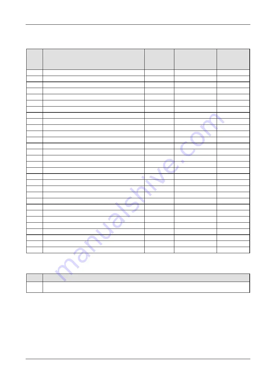
Fieldbus connector X2 for COM-CN-EN 

Pin 

Signal 

Symbol 

Type 

Pin at Fieldbus

connector 

RJ45 

1  


Ethernet, Receive Data N 

EN_IN 

MAC Input neg. 

Note 1 

3  


Ethernet, Receive Data P 

EN_IP 

MAC Input pos. 

Note 1 

5  


Ethernet , Transmit Data N 

EN_ON 

MAC Output neg. 

Note 1 

7  


Ethernet, Transmit Data P  

EN_OP 

MAC Output pos. 

Note 1 

9  


10  


11  


12  


13 

LINK-LED, active low 

LNK# 

4 mA Output 


14 

SYS-LED, RUN, Cathode green LED 

RUN# 

4 mA Output 


15 

ERR-LED, active low 

ERR# 

4 mA Output 


16 

SYS-LED, RDY, Cathode yellow LED 

RDY# 

4 mA Output 


17 Ground 

GND 


18 

Power Supply 

+3.3 V 


19 

Peripheral IO 

PIO 

LVTTL Input / Output   

20 

Don't use - needed for isolation 


21 

Don't use - needed for isolation 


22  


23 

Transmit Data + 

TX+ 


24 

Transmit Data - 

TX- 


25 

Receive Data + 

RX+ 


26  


27  


28 

Receive Data - 

RX- 


29  


30  


Table 20: Fieldbus Connector X2 for Ethernet 


Note 

Information 

Ethernet Signals could be only used without the hardware interface on the COM. Ask for special customer ver-
sion. 

Table 21: Notes for Fieldbus Connector X2 for Ethernet  


Summary of Contents for COM-C Series

Page 1: ...Design Guide COM C Communication Module Hilscher Gesellschaft f r Systemautomation mbH www hilscher com DOC021001DG12EN Revision 12 English 2011 06 Released Public...

Page 2: ...3 3 Fieldbus Connector X2 for DeviceNet Master Slave 37 3 3 4 Fieldbus Connector X2 for PROFIBUS Master Slave 38 3 3 5 Fieldbus Connector X2 for Ethernet 39 3 3 6 Fieldbus Connector X2 for CC Link Sl...

Page 3: ...C Communication Module DOC021001DG12EN Revision 12 English 2011 06 Released Public Hilscher 2002 2011 7 Technical Data 59 7 1 Product Tests 61 8 Appendix 63 8 1 List of Tables 63 8 2 List of Figures...

Page 4: ...ion on various host sys tems Through the set of standard application interfaces and the same board dimensions in each COM family it is easy to switch between the different fieldbus systems e g PROFIBU...

Page 5: ...een COM and COMX Comparison of supported protocols for COM C and COMX C COM C COMX C AS Interface Master supported in preparation CANopen Master supported supported CANopen Slave supported supported C...

Page 6: ...0100084 update M0600121 new M0900102 new M0200402 kept Section Mounting of COM C Modules expanded 4 bolt types Section SYNC Signals added Section Signal Overview and Pinning of the Fieldbus Connector...

Page 7: ...s USB Table 74 Hardware Revision of COMX Modules with new USB Interface updated Table 75 Hardware Revision of COMX Modules with old USB Interface updated German text replaced by English text in the fo...

Page 8: ...memory with 8 bit bus width 3 3 V power supply reduce power consumption Available in extended temperature specification With the COM C we have a much more compact form factor and additional technical...

Page 9: ...e dual port memory which can be easily integrated as a static memory device It has a non multiplexed 8 bit data bus with several control lines to the host system Between the COM C Module and the host...

Page 10: ...the documentation were created for the use of the products by qualified experts however errors cannot be ruled out For this reason no guarantee can be made and neither juristic responsibility for erro...

Page 11: ...ms Use of the software in such an environment occurs at your own risk No liability is assumed for damages or losses due to unauthorized use 1 4 4 Warranty Although the hardware and software was develo...

Page 12: ...eviceNet Slave angled COM CA DNM DeviceNet Master angled COM CA EN Ethernet angled COM CA EIS EtherNet IP Slave angled COM CA IBS INTERBUS Slave angled COM CA DPS PROFIBUS DP Slave angled COM CA DPM P...

Page 13: ...d of the edge of printed circuit board of the COM Module The COM CN Module has to be used if the mechanical dimensions or order of the LEDs switches and fieldbus connector doesn t fit In that case you...

Page 14: ...a should be less than 330 maw For further Module development please reserve additional 10 mm space behind the Module There are a few larger fieldbus interfaces which do not fit on the small board spac...

Page 15: ......

Page 16: ......

Page 17: ......

Page 18: ......

Page 19: ......

Page 20: ...ww samtec com Cheaper version 50 pin Connector TFM 125 02 S D A TFC 125 02 F D A 30 pin Connector TFM 115 02 S D A TFC 115 02 F D A Note Datasheet of SAMTEC TFM connector see next page Please notice t...

Page 21: ......

Page 22: ...al blocks there are a M2 5 thread to mount a front panel directly on the Module This allows to have the same cutting in the device housing for all types of Modules Use fine technology that means six m...

Page 23: ...de COM CA AS CCS CO DN DP EN IBS SCEB COM CA B20X5 COM CA B20X5 COM CN AS CCS CO DN DP EN IBS COM CA B20X5 COM CA B20X5 Table 7 Usage of Bolt for COM Modules The drawings for the bolts are shown on th...

Page 24: ......

Page 25: ......

Page 26: ......

Page 27: ......

Page 28: ...esignation of the COM C Each COM C Module has a matrix code label A matrix label contains 3 items 1 Part number 2 Hardware Revision 3 Serial number The figure shows part number 1521 416 hardware revis...

Page 29: ...figure shows the meaning of the rotary switch for COM CA DPS COM CA COS and COM CA DNS The rotary switches are to set the bus address Figure 4 Meaning of the Rotary Switch The following figure shows...

Page 30: ...002 2011 3 Host Interface Attention All COM modules have an operation voltage of 3 3 V which reduces the power con sumption Therefore the voltage levels of the signals have to be not higher than 3 3 V...

Page 31: ...Input 15 Request to Send Serial line RTS1 LVTTL Output 16 Clear to Send Serial line CTS1 LVTTL Input 17 reserved for future don t connect 18 reserved for future don t connect 19 Receive Data Diagnosti...

Page 32: ...TTL Input Output 42 Data line 6 D6 LVTTL Input Output 43 Data line 5 D5 LVTTL Input Output 44 Data line 4 D4 LVTTL Input Output 45 Data line 3 D3 LVTTL Input Output 46 Data line 2 D2 LVTTL Input Outpu...

Page 33: ...for future don t connect 17 Interrupt active low INT1 LVTTL Output 18 reserved for future don t connect 19 reserved for future don t connect 20 reserved for future don t connect 21 Reset active low R...

Page 34: ...Input Output 42 Data line 6 D6 LVTTL Input Output 43 Data line 5 D5 LVTTL Input Output 44 Data line 4 D4 LVTTL Input Output 45 Data line 3 D3 LVTTL Input Output 46 Data line 2 D2 LVTTL Input Output 47...

Page 35: ...tput Note 1 13 COM LED STA Cathode yellow LED STA 4 mA Output 14 SYS LED RUN Cathode green LED RUN 4 mA Output 15 COM LED ERR Cathode red LED ERR 4 mA Output 16 SYS LED RDY Cathode yellow LED RDY 4 mA...

Page 36: ...Cathode green LED RUN 4 mA Output 15 COM LED ERR Cathode red LED ERR 4 mA Output 16 SYS LED RDY Cathode yellow LED RDY 4 mA Output 17 Ground GND 18 Power Supply 3 3 V 19 Peripheral IO PIO LVTTL Input...

Page 37: ...t 14 RUN LED RUN Cathode green LED RUN 4 mA Output 15 MNS LED active low Cathode red LED MNS_CR 4 mA Output 16 SYS LED RDY Cathode yellow LED RDY 4 mA Output 17 Ground GND 18 Power Supply 3 3 V 19 Per...

Page 38: ...de green LED RUN 4 mA Output 15 COM LED ERR Cathode red LED ERR 4 mA Output 16 SYS LED RDY Cathode yellow LED RDY 4 mA Output 17 Ground GND 18 Power Supply 3 3 V 19 Peripheral IO PIO LVTTL Input Outpu...

Page 39: ...pos Note 1 9 10 11 12 13 LINK LED active low LNK 4 mA Output 14 SYS LED RUN Cathode green LED RUN 4 mA Output 15 ERR LED active low ERR 4 mA Output 16 SYS LED RDY Cathode yellow LED RDY 4 mA Output 17...

Page 40: ...Note 1 9 10 11 12 13 COM LED STA Cathode yellow LED STA 4 mA Output 14 SYS LED RUN Cathode green LED RUN 4 mA Output 15 COM LED ERR Cathode red LED ERR 4 mA Output 16 SYS LED RDY Cathode yellow LED R...

Page 41: ...S to high level Then the COM C Modules begins with the program execution and initialization This power up time is different for each COM C Module Normally the time is about less than two seconds The C...

Page 42: ...terface can support 16 Bit you should connect the WIF signal to ground If not please let this uncommitted that 16 Bit modules will work in a compatible 8 Bit mode In case of a 16 Bit system you have t...

Page 43: ...oblem the external accesses to the EC1 Dual port memory are internally synchro nized to the EC1 memory cycle This technique actually removes the possibility of the EC1 and the external interface acces...

Page 44: ...G12EN Revision 12 English 2011 06 Released Public Hilscher 2002 2011 3 4 9 Timing Diagram of COM C Figure 6 COM Timing Diagram of a Read Cycle at the Dual Port Memory Figure 7 COM Timing Diagram of a...

Page 45: ...0 8 ns with 48 MHz CLK Notes Both CS and RD resp CS and WR must be low to start a Dual port memory cycle If the CS signal is going low or held low the BUSY signal goes also low Then after some clock c...

Page 46: ...Port Memory for COM CA SCEB The connection of the COM CA SCEB can be done like for the other COM C The timing is a little bit different because of the used SERCON 816 protocol interface chip Please as...

Page 47: ...e shows an example for a connection of a COM C Module directly to a micro processor The signal lines of the COM C Module are directly connected to the microprocessor AM80C188ER which runs with 3 3 V F...

Page 48: ...s If there is no definition in the fieldbus standard we use red for error and yellow for status If there is a definition we use these for the functions and colors of that LED For the Modules described...

Page 49: ...used firmware On depends on used firmware red Flashing depends on used firmware red green Flashing depends on used firmware NET Off depends on used firmware Table 26 LED Ethernet COM 3 times fast at 5...

Page 50: ...green Flashing cyclic at 5Hz No error in the configuration found communication is stopped or ready for communication but no connection to any Slave green Flashing irregular Power Up Configuration mis...

Page 51: ...vice sends a telegram red On Device has detected a communication problem to at least one CANopen Node COM Off Device is ready to receive or is receiving telegrams Table 29 LED CANopen Master COM 3 tim...

Page 52: ...ion found communication is stopped or ready for communication but the device has no cyclic data exchange with the CC Link Master green Flashing irregular Power Up Configuration missing or faulty devic...

Page 53: ...rk error duplicate MAC ID or bus off red Flashing Connection timeout red green Flashing Communication faulted state MNS Off Not powered not online Table 32 LED DeviceNet Master COM 3 times fast at 5 H...

Page 54: ...ommunication to the IBS Master is possible RC green Off Communication to the IBS Master is not possible On Master active user data is exchanged Flashing irregular Communication is not possible system...

Page 55: ...ation problem to at least one PROFIBUS DP Slave or has detected a short circuit COM Off Device is not configured or has not received the Token permission on the PROFIBUS network Table 35 LED PROFIBUS...

Page 56: ...eleased Public Hilscher 2002 2011 4 1 12 SERCOS optical LED Color State Meaning On Device is powered and not in reset state RDY yellow Off Device is not powered or in reset state On or Flashing Commun...

Page 57: ...itch to set up the device address on board If the Module COM CN is used for slave the address can be set by software over the dual port memory Note This feature is not available at the CC Link Module...

Page 58: ...e transmit and receive signals to use with an RS232C interface for di agnostic purpose Over this diagnostic line you can download a new firmware configuration files or make only diag nostic during run...

Page 59: ...ting current mA COM Cx ASM U1 U3 280 mA 50 mA 400 mA 70 mA COM Cx COS COM Cx COM U1 240 mA 400 mA COM Cx DNS COM Cx DNM U1 U2 170 mA 20 mA 300 mA 55 mA COM Cx EN U1 310 mA 400 mA COM Cx DPM U1 340 mA...

Page 60: ...6 2 1999 Industrial Environment EN 61000 4 2 EN 61000 4 3 EN 61000 4 4 EN 61000 4 5 EN 61000 4 6 Details are listed in chapter Product tests Emission EN 61000 6 4 EN55011 Table 39 Technical Data EMC...

Page 61: ...GND to PE 1 kV 12 Ohm 9 F B Power Supply lines 24V only Differential mode 24V to GND 0 5 kV 2 Ohm 18 F B EN 51000 4 5 Communication lines shielded 1 kV 2 Ohm 18 F B Conducted Immunity Power supply li...

Page 62: ...24h 85 70 C 24h 85 non condensing A IEC 60068 2 1 Ab Cold withstand Min storage temperature standard extended 25 C 24h 40 C 24h A IEC 60068 2 2 Bb Dry heat withstand Max storage temperature standard e...

Page 63: ...ink Slave 40 Table 24 Function Table of the 16 Bit Decode Logic 42 Table 25 Symbols for COM Timing Diagram of a Read respectively Write Cycle at the Dual Port Memory 45 Table 26 LED Ethernet COM 49 Ta...

Page 64: ...Support Phone 33 0 4 72 37 98 40 E Mail fr support hilscher com India Hilscher India Pvt Ltd New Delhi 110 025 Phone 91 11 40515640 E Mail info hilscher in Italy Hilscher Italia srl 20090 Vimodrone M...

Reviews: