background image


APEX

 Exciter Incorporating FLO

 Technology

Maintenance and Troubleshooting

Exciter Troubleshooting Flow Charts

Page: 5-14

888-2604-001

03/08/07

WARNING: Disconnect primary power prior to servicing.

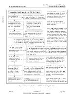
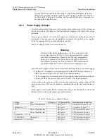
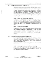
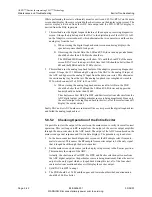
Figure 5-7  Transmitter Fails Mask Test Troubleshooting Flow Chart

Transmitter Fails Mask Test

N

Y

N

Y

This mode must be active for exciter 
to perform non-linear correction, 
which effects mask performance, See 
Note 1.

Note 3: Refer to the technical manuals 
for your transmitter to determine exact 
RF feedback connections. Chapter 2 
shows typical RF feedback connec-
tions for various Harris transmitters. 

Is transmitter PA RF sample connected to exciter? See 
Note 3. Is this sample at the correct level, see Note 4. This 
sample is necessary for exciter to perform non-linear 
correction, which effects mask performance.

Is exciter RTAC Non-Lin 
correction in Adapt 
mode? See exciter Main 
Screen.

Are the status screen 
diagnostics function all 
set to normal? SeeTable 
5-1, on page 5-10

If one or more diagnostic functions are 
active, normal operation of exciter may 
be impaired. 

At this point, obvious causes of problem 
have been eliminated. Call Technical 
Support.

Section 5.7.3, Checking 
Transmitter Spectrum, on 
page 5-18 can be used to 
determine stage where 
shoulder response has failed. 
See Note 6.

Note 1: See RTAC in Section 3.2, 
Starting Point: The Main LCD Touch 
Screen, on page 3-2

Is transmitter operating at or 
below its rated output 
power, and is it correctly 
calibrated?

N

Y

Check RF output power calibration of 
transmitter. If RF system is overdriven, 
its resultant non-linearity may be outside 
of RTAC correction range

Is the Status > Adaptive 
Processing screen normal? 
See Figure 3-7, on page 3-9

N

Y

This screen shows the PA feedback 
sample level, see Notes 2. Is this 
feedback sample out of range or 
Faulted?

Note 2: In Adaptive Processing status 
screen, PA Feedback and ADT 
Overrange functions should show OK. 
The Yellow and Blue horizontal Bars 
represent RF sample level. They 
should fall within middle 2/3rds of box 
if their levels are correct. Yellow = 
average level and blue = peak level. 
Refer to Section 3.4.3, Adaptive 
Processing Board Status Screen, on 
page 3-9 for 
additional information.

Note 4: The correct sample input 
power range, measured at the at the 
exciter rear panel sample input cable, 
is -30 to 0 dBm. 

Is transmitter’s RF PA system is faulty? 
If so, resultant non-linearity may be 
outside of RTAC correction range. 

Y

Note 5: This problem could be caused 
by the exciter Chart Source (RF 
spectrum display) selection not being 
set to Tx-Pre HPF or Tx Post HPF. 
This screen is found under Setup > 
Setup Screen > Display Setup. For 
more information, see Section 3.6.4, 
Display Setup Screen, on page 3-41.

If linearity still looks bad at transmitter 
output but looks good on exciter screen, 
see Note 5.

N

N

Y

Filter Type: 

Use FLO BANDPASS 

because of the application of this exciter. 

Use 

Standard

 if the standard D-Mask filter is used. 

Use Asymm

 (asymmet-

rical) if the sharp tuned filter (sometimes called “Cool Fuel”) is used or if the 
group delay for the transmitter is not symmetrical, such as when its output is 
reflected through an adjacent channel sharp tuned filter in order to combine 
the two transmitters. 

Exciter must be restarted

 to make filter change active.

In the Setup > RTAC Setup 
screen, does the Filter Type 
choice match the HPF in the 
transmitter System?

Y

Note 6: Shoulders refers to the 
spectral response just outside the 
channel limits.

Summary of Contents for APEX

Page 1: ...T M No 888 2604 001 Copyright Harris Corporation 2007 All rights reserved Printed January 25 2007 Revision A 03 08 07 TECHNICAL MANUAL APEXTM Exciter Incorporating FLOTM Technology 888 2604 001...

Page 2: ...not damaged Locate and retain all PACKING CHECK LISTs Use the PACKING CHECK LIST to help locate and identify any components or assemblies which are removed for shipping and must be reinstalled Also r...

Page 3: ...logy 2604ti fm March 8 2007 888 2604 001 Page i WARNING Disconnect primary power prior to servicing MANUAL REVISION HISTORY APEX Exciter Incorporating FLO Technology 888 2604 001 Rev Date ECN Pages Af...

Page 4: ...APEX Exciter Incorporating FLO Technology Page ii 888 2604 001 March 8 2007 WARNING Disconnect primary power prior to servicing...

Page 5: ...gnators for the item i e C001 R102 etc that corresponds to the number found in the schematics C001 in a bill of material is equivalent to C1 on the schematic or 2 gives added information or further ex...

Page 6: ...APEX Exciter Incorporating FLO Technology Page iv 888 2604 001 March 8 2007 WARNING Disconnect primary power prior to servicing...

Page 7: ...equipment local building codes and fire protec tion standards must be observed The following National Fire Protection Association NFPA standards are recommended as reference Automatic Fire Detectors N...

Page 8: ...APEX Exciter Incorporating FLO Technology Page vi 888 2604 001 March 8 2007 WARNING Disconnect primary power prior to servicing...

Page 9: ...as required D Arrange transportation to a hospital as quickly as possible E If arms or legs are affected keep them elevated NOTE If medical help will not be available within an hour and the victim is...

Page 10: ...APEX Exciter Incorporating FLO Technology Page viii 888 2604 001 March 8 2007 WARNING Disconnect primary power prior to servicing...

Page 11: ...y Requirements 2 4 2 5 2 Typical Transmitter Systems Block Diagrams 2 4 2 5 3 Atlas Mobile Transmitters 2 5 2 5 3 1 Atlas Mobile Transmitter 1 PA Cabinet 2 Exciters 2 5 2 5 3 2 Atlas Mobile Transmitte...

Page 12: ...tatus Screen 5 5 3 18 3 4 5 IF RF Processing Status Screens 3 19 3 4 5 1 UDC Interface Board Status Screen 1 4 3 19 3 4 5 2 PLL Board Status Screen 3 20 3 4 5 2 1 PLL Diagnostics 3 21 3 4 5 3 Up Conve...

Page 13: ...Configure 1 5 3 48 3 6 7 2 FPGA Configure 2 5 3 49 3 6 7 3 FPGA Configure 3 5 3 50 3 6 7 4 FPGA Configure 4 5 3 51 3 6 7 5 FPGA Configure 5 5 Restore Defaults 3 52 3 6 8 Change Passwords Security Setu...

Page 14: ...5 2 Digital Deck Power 4 14 4 5 2 1 Controller Board Power 4 14 4 5 2 2 FPGA Modulator Board Power 4 15 4 5 2 3 Adaptive Processing Board Power 4 15 4 5 2 4 Power for DAC and ADC Boards 4 15 4 5 2 5...

Page 15: ...4 ASI Transport Stream Faults 5 18 5 8 Exciter Troubleshooting 5 19 5 8 1 Frequency Error 5 19 5 8 2 Dark Screen 5 19 5 8 3 Power Supply Voltages 5 20 5 8 4 Troubleshooting Down to the Board Level 5...

Page 16: ...APEX Exciter Incorporating FLO Technology Table of Contents Page xiv 888 2604 001 03 08 07 WARNING Disconnect primary power prior to servicing...

Page 17: ...us Screen 3 9 Figure 3 8 Adaptive Processing Diagnostics 3 11 Figure 3 9 Modulation Board Status Screen 3 12 Figure 3 10 Modulation Board Status Screen 1 2 3 12 Figure 3 11 ADC and DAC Status Screen 2...

Page 18: ...2 Figure 4 2 APEX Exciter Signal Flow Block Diagram 4 4 Figure 4 3 The 44 4 MHz Phase Lock Loop 4 6 Figure 4 4 Exciter Output Spectral Response RTAC Bypassed 4 7 Figure 4 5 Up Converter Simplified Blo...

Page 19: ...8 07 888 2604 001 Page xvii WARNING Disconnect primary power prior to servicing Figure A 1 Tera Term Pro Screen When Connected to Exciter A 2 Figure A 2 Stop Action Capture of Screen Down Load Scroll...

Page 20: ...APEX Exciter Incorporating FLO Technology List of Figures Page xviii 888 2604 001 03 08 07 WARNING Disconnect primary power prior to servicing...

Page 21: ...3 2 Location of System Setup Sub Screens 3 33 Table 3 3 Settings Resulting From Restore Defaults Activation 3 33 Table 3 4 UHF External I O Parallel Control Interface Connector J1 3 44 Table 4 1 Outpu...

Page 22: ...APEX Exciter Incorporating FLO Technology List of Tables Page xx 888 2604 001 03 08 07 WARNING Disconnect primary power prior to servicing...

Page 23: ...l distortions which occur in the transmitter RF power amplifiers high power filter and transmission line This APEX exciter incorporating FLO Technology is presently installed in the Harris Ranger and...

Page 24: ...es from the rear and forced over the circuits The top and bottom covers may be removed to provide access to the digital and analog circuit boards however there are no adjustments on the circuit boards...

Page 25: ...xciter Incorporating FLO Technology Physical Description Introduction 2604s100 fm 03 08 07 888 2604 001 Page 1 3 WARNING Disconnect primary power prior to servicing Figure 1 2 APEX Exciter Front Panel...

Page 26: ...ncy precision and or accurate super frame timing for use with wide area single frequency network operation The exciter uses RTAC Real Time Adaptive Correction to monitor and manage pre correction for...

Page 27: ...dance is 50 ohms Table 1 2 Harris APEX Exciter Service Conditions Specifications Specification Explanation Ambient temperature 0 to 50 celsius 32 to 122 fahrenheit Ambient humidity 0 to 90 relative no...

Page 28: ...0 8 per 24 hours with no external reference 1 x 10 9 for SFN single frequency network with external reference Response variation 0 2 dB with the exciter in loopback mode Group delay 2 nsec with the ex...

Page 29: ...be carefully studied before attempting to operate the exciter or check the exciter setup against the factory final test data 2 3 Signal Connections Most of the input and output connections are at the...

Page 30: ...LAN 10Base T is a provision for connecting the exciter to a local area network RS232 on front and rear panels of exciter is a 9 Pin D interface connector They are used to communicate with various comp...

Page 31: ...vel of 30 to 0 dBm average RF power The HPF sample monitors the output of the high power mask filter It uses this sample to characterize the amplitude response and group delay response of the filter F...

Page 32: ...o the rear panel The correction algorithms like any feedback loop will drive the error to zero at the measurement point which is at the rear panel Use only a high quality 50 ohm coax such as RG223 Avo...

Page 33: ...binet Atlas Mobile transmitter system is shown in Figure 2 3 It has dual exciters with the RF sample feedback connections shown Samples for each exciter are provided by two way zero phase splitters in...

Page 34: ...upler The PA sample is taken from the cabinet combiner output coupler If the transmitter system has dual exciters feedback samples for each exciter are ob tained by splitting each sample cable as show...

Page 35: ...t the two RTAC functions These refer to the two RF feedback signals which are connected to the rear panel of the exciter These settings determine how the exciter will pre correct for the transmitter s...

Page 36: ...ation Power calibration is covered in Section 3 6 2 1 on page 3 38 Main Screen Setup RTAC Setup Can be used to avoid nuisance overdrive trips Is used to determine RTAC startup mode when the exciter or...

Page 37: ...on the front panel Transport Stream hardware switch it will light green If both are missing the front panel Transport Stream and the Digital Processing hard ware switches will show faults light red Ma...

Page 38: ...n Table 5 1 on page 10 The following is a list of the normal states of the more critical diagnostic functions and the exciter mute Status Adaptive Processing Diagnostics LoopBack None Test Tones Disab...

Page 39: ...ZFSC 4 1 zero phase 50 ohm BNC Harris part number 620 2833 000 Used as needed to split or combine an RF signal Adapters N female to BNC male Harris part number 620 0128 000 Used to connect a BNC coupl...

Page 40: ...APEX Exciter Incorporating FLO Technology Installation Materials Needed Page 2 12 888 2604 001 03 08 07 WARNING Disconnect primary power prior to servicing...

Page 41: ...of the output power display On the main screen output power can also be set by touching the numbers in the power display This brings up a number pad where a new value for output power between 0 and 2...

Page 42: ...o should range from 30 to 45 dB Error vector magnitude EVM does not apply to the Apex Flo exciter Integrated power of the lower sideband LSB and upper sideband USB over the spectrum of the lower and u...

Page 43: ...w RTAC Digital signal taken at output of adaptive precorrector board BIT Sample of the Built In Test FIFO for future use Exciter RF signal is taken from J4 sample output of exciter PA and connected to...

Page 44: ...near distor tions caused by the filters tuned circuits and other amplitude response shaping cir cuits in the transmitter system These distortions are frequency response errors called amplitude on the...

Page 45: ...w Chart Main Screen Power Up Screen Setup Fault Note Selecting Home from any screen Selecting Fault from any screen Expanded Display Screen Status Displays returns to the Main Screen returns to the Ex...

Page 46: ...Board Screen 1 of 5 Controller Board Screen 2 of 5 External I O Board Screen 3 of 5 CAN Status returns to the Main Screen returns to the Exciter Status Screen Selecting Status in any Status Screen re...

Page 47: ...o the Exciter Status Screen System Setup Screen See page 3 32 Screen 1 of 2 Exciter Setup See page 3 35 RTAC Setup See page 3 38 Display Setup See page 3 41 Power Calibration See page 3 38 External I...

Page 48: ...n These boxes represent circuit boards or control areas within the exciter see names in Table 3 1 The general status of each section OK or FAULT is displayed to the right of each box Touching any of t...

Page 49: ...Status Screen The Transport Stream Status screen is shown in Figure 3 6 with screen entries listed below TS 1 Detect This selection indicates OK if the transport stream is present at the trans port st...

Page 50: ...lowable level Each of the feedbacks listed below has a bar graph The yellow upper bar indicates average power level and the blue lower bar indicates peak level The presence of an RF sample which is wi...

Page 51: ...input bit stream back to replace the A D converter output bit stream It tests the modulator and corrector boards Analog loops the 11 1 MHz IF output from the D A board to the IF input of the A D boar...

Page 52: ...atus selection offers two selections which are The Modulator which consists of screen 1 the FPGA Modulator and screen 2 which gives the software revisions of the ADC DAC Boards See Modulator Board Sta...

Page 53: ...the configuration of the FPGA which is a microprocessor FPGA prog OK or FAULT refers to the programing of the FPGA board EEPROM Ok or FAULT The EEPROM is the local board memory It stores board specifi...

Page 54: ...Active or TS2 Active if one or both streams are connected to the two ASI inputs on the exciter rear panel The presence of one or both of the transport streams in indicated in the TS1 and TS2 Detect in...

Page 55: ...th selected as show in the table be low SSF Arrival displayed in milliseconds Ave Frequency Error In Hz GPS 1PPS Loss YES in red indicates loss of GPS 1PPS NO in black indicated signal is present The...

Page 56: ...nsport Stream Status screen are as follows TS1 Detect Yes or No TS2 Detect Yes or No Yes transport stream present No in red transport stream missing TS1 LOF Yes or No TS2 LOF Yes or No Yes in red faul...

Page 57: ...The parameters of the SFN FIFO Status screen are as follows Core Stall YES in red indicates error NO in black indicated OK Overflow YES in red indicates error NO in black indicated OK Underflow YES in...

Page 58: ...een 5 5 The parameters of the SFN FIFO Status screen are as follows Ver Err YES in red indicates error NO in black indicated OK Pkt Miss Count Displayed as an integer decimal Dropped Groups Displayed...

Page 59: ...5 1 UDC Interface Board Status Screen 1 4 UDCInterfaceStatus bmp Figure 3 17 UDC Interface Board Status Screen 1 4 The UDC Interface Board screen is shown in Figure 3 17 with screen entries listed be...

Page 60: ...r from UDC interface board via connector J1 15 Vdc Input power from UDC interface board via connector J1 8 Vdc Input power from UDC interface board via connector J1 IF PLL Lock YES or NO This PLL shou...

Page 61: ...Reference entry is labeled Yes The Xtal Aging crystal oscillator aging control is used to set the frequency of the internal 10 MHz crystal oscillator when no external reference is used The initial se...

Page 62: ...r output power level is set from the ex citer main screen or the extended control This is the normal setting When disabled for test purposes the exciter output power is locked in the previous enabled...

Page 63: ...his soft key will restore the default values to tune A and tune B When tune A and or tune B values are changed they are automatically saved and will not revert to the default values after the exciter...

Page 64: ...Source is set to monitor the exciter During each sample period the first action is to adjust the down converter gain to provide the A D converter with an IF signal of the correct amplitude During the...

Page 65: ...the bottom of the screen The possible range is 0 4096 Sample levels can be viewed on the Adaptive Processing Screen RF Sample tells which down converter RF input sample is currently active RF Level T...

Page 66: ...s of the internal PLL of the MPC823 micro controller on the controller board It indicates the internal 75 MHz clock is locked to the 32 768 KHz crystal oscillator Board Rev Board revision for the Cont...

Page 67: ...egisters are required to handle the 16 status channels These entries are used for factory testing Foldback This in an analog input which tells the percent of exciter output power fold back typically d...

Page 68: ...cal board memory It stores board specific information such as board type board revision CPLD revision and other lo cal data Note Within any of these screens touching Home returns to the main screen an...

Page 69: ...f a volt of 2 Vdc analog inputs 2 and 4 will measure within a few tenths of a volt of 3 Vdc The VSWR foldback percentage will be based on the relative value of the loopback voltage VLB compared to the...

Page 70: ...bmp Figure 3 27 CAN Bus Status Screen Information about the Can Status screen will be provided later 3 4 6 3 1 CAN Diagnostics A CAN Test Message is available on the CAN Diagnostics screen This funct...

Page 71: ...information such as time and position shown on the screen but to do so the receiver must track three satellites The screen shows the number of visible satellites and the number of tracked satellites...

Page 72: ...window appears The message in this window is Starting BIT requires exciter to be muted If the Ok soft key is pressed the exciter RF output is reduced to zero If the cancel soft key is pressed the exci...

Page 73: ...a selection An alpha numeric key pad is displayed when a title is needed 3 6 1 Restore Defaults Operation Main Screen Setup System Setup screen Restore Defaults soft key function effects the followin...

Page 74: ...ommon but customer s choice RF Present Cutoff 10mW 50 of normal exciter output power Serial Setup page 1 RS 232 Front and Rear See Section 3 6 6 1 Serial Setup Screen 1 of 3 RS 232 on page 3 45 Baud R...

Page 75: ...GPS receiver use External is the normal mode If used it requires an external 1PPS input at the rear panel connector Loss of the 1PPS will cause a Digital Status hardware switch fault lights red and t...

Page 76: ...Harris Atlas series UHF digital transmitters Waveguide Type For UHF frequencies enter the type of waveguide used between the HPF and the antenna Selecting a type and length of waveguide allows RTAC to...

Page 77: ...actor by 0 5 dB intervals and stop when the shoulder level rises 5 Raise the Max Mod Crest Factor 0 5 dB above this point This is the correct set ting Mute soft key on right side of screen Mute When E...

Page 78: ...on the right side of the screen in Figure 3 32 activates the exciter RF output power calibration procedure The power calibration is accomplished by connecting an accurate power meter to the RF output...

Page 79: ...nsmitter maintenance and etc They are good for comparative testing Filter Set selections include 1 through 4 Filter Title Brings up an alpha numeric touch keypad to enter the name for the select ed fi...

Page 80: ...roduce a peak stretch up to a 3 dB limit Nuisance overdrive trips can be avoided by programming the maximum peak stretch parameter of the RTAC Setup Screen The maximum peak stretch is adjustable from...

Page 81: ...a list of entries on the System setup screen Date Enter the current date Time Enter the correct time The exciter will keep track of the date and time even during periods of power loss and display the...

Page 82: ...e LCD display numeric key pad 3 6 5 External I O Setup Screen Some functions of the APEX digital exciter must be capable of being controlled operated via a parallel remote control system while other f...

Page 83: ...ter output power from the normal exciter output power level VSWR F B input voltage below the low threshold down to the preset maximum allowable exciter output power reduction when the VSWR F B input v...

Page 84: ...ng and channel to input output connector J1 assignments are fixed A list of channel entries J1 pin assignments corresponding channel numbers and the function input or output and its description is lis...

Page 85: ...Setup Screen 1 of 3 RS 232 The purpose of the Serial Setup screen is to program the serial ports on the front and rear panel of the exciter Since the setup parameters for the front and rear connector...

Page 86: ...er A the IP address is 192 168 217 200 For exciter B the IP address is 192 168 217 201 The IP addresses for eCDi units with software revisions earlier than 2 6 are as follows For exciter A the IP addr...

Page 87: ...as follows Default is 1Hz Rate for PowerCD Diamond and SigmaCD transmitters is 2 Hz Improper Baud or Tx Frame rates will lock up the CAN bus The solution to this problem is to set the rates correctly...

Page 88: ...FPGA when changed through the GUI No FPGA re initialization occurs when any of these registers are changed The parameters of the FPGA Configure 1 5 screen are as follows Transmitter ID Unsigned 16 bi...

Page 89: ...s with a range 0 to 2000 When the GPS 1PPS signal loss shown in the Main Screen Status Digital Pro cessing FLO FPGA Registers GPS and Clock Status screen exceeds the 1PPS Mute Delay time the GPS 1PPS...

Page 90: ...ons NTWK Geog Delay Time in microseconds see below for calculations The value for Transmitter Delay shall be displayed in integer microseconds with a valid range and the value for the FPGA register va...

Page 91: ...s follows Bandwidth 5MHz 6MHz 7MHz 8MHz National Length Unsigned Decimal range dependent on bandwidth 0 245 5MHz 0 295 6MHz 0 345 7MHz 0 395 8MHz Pos Pilot Length 2 6 10 14 not bandwidth dependent WID...

Page 92: ...efaults Initialize FPGA Save as Defaults Restore Factory Defaults loads all FPGA registers with the values defined as default initialization values in the API if defined followed by a re initializatio...

Page 93: ...ure 3 46 on page 3 54 if it is locked The frequency select and frequency offset entries on the exciter setup screen are locked when the diagnostics setup is locked If either password change screen is...

Page 94: ...up functions will remain unlocked If Ok is selected the user setup functions will be locked To gain access to the setup functions the System Setup User Setup Locked screen must be entered This time an...

Page 95: ...being tested 3 6 9 Restore Defaults The restore defaults soft key on the System Setup screen see Figure 3 46 is locked under the Factory Setup password 3 7 RTAC Operating Procedures Main Screen RTAC...

Page 96: ...hich down converter sample is currently active RF Level RF level taken after the AGC circuit for the current sample It typically ranges between 0 5 to 1 0 Vdc for samples of proper input power range I...

Page 97: ...nd etc They are good for comparative testing of the transmitter and RTAC correction Filter Set selections include 1 through 4 Filter Title Brings up an alpha numeric touch keypad to enter the name for...

Page 98: ...APEX Exciter Incorporating FLO Technology Navigating the LCD Display Screens RTAC Operating Procedures Main Screen Page 3 58 888 2604 001 03 08 07 WARNING Disconnect primary power prior to servicing...

Page 99: ...n top performance Control and monitoring of the exciter is provided by a front panel display and remote control connection and in some transmitters exciter control is also extended to the trans mitter...

Page 100: ...e signal following the modulation and spectral filtering processes Two down converted samples from various locations along the transmitter system are compared the output of the modulator board to shap...

Page 101: ...troller board controls all of the other boards except the power supply and the fan It indirectly controls the output amplifier through the APC automatic power control and the mute function A built in...

Page 102: ...verted RF Switch Down Converter Board PLL Board 1st L O 2nd L O 10 MHz Reference Exciter Sample Input PA Sample Input HPF Sample Input Exciter RF Output DAC ADC Adaptive Precorrector Board FPGA Modula...

Page 103: ...PM conversion Non linear distortion causes intermodulation products to appear within the signal pass band and in the adjacent channels making it difficult or impossible for the transmitter to pass th...

Page 104: ...set to 6 MHz The available bandwidth settings are 5 6 7 and 8 MHz For each setting the actual signal bandwidth is approximately 0 5 MHz less than the indicated bandwidth the actual bandwidth for each...

Page 105: ...A2 Output Amplifier board A5 Down Converter board Refer to Figure 4 2 for a block diagram of the APEX exciter The up converter accepts a 11 1 MHz IF from the DAC digital to analog converter board A12...

Page 106: ...ut of the up converter is a low level on channel signal This signal is sent to the output amplifier 4 4 1 1 Up Converter Board UHF VHF Band Pass Filter The type of filter used depends on the operating...

Page 107: ...F high power filter output The RF level for each sample should be within a range of 30 to 0 dBm average power where the RF sample cables enter the rear panel connectors of the exciter The controller b...

Page 108: ...method is via a control voltage form the DAC The DAC number is supplied from the controller board and locks the 10 MHz oscillator to the 1 PPS pulse per second output of a GPS Satellite This is the m...

Page 109: ...DDS direct digital synthesis based oscillator which is clocked at 400 MHz The 400 MHz is generated in a single loop PLL phase locked loop which is locked to the 10 MHz reference oscillator Figure 4 8...

Page 110: ...equency range This chosen frequency is applied to a divide by N circuit where N is chosen so that its output or a harmonic of its output falls on the desired second LO frequency A tunable bandpass fil...

Page 111: ...1 then to relay K1 which routes the output to the RF output jack J2 when the exciter is unmuted and to the RF load output jack J3 when muted Directional coupler DC1 samples the forward power of the am...

Page 112: ...wer for the digital lower deck of the exciter enters the controller board at J6 J6 is mounted on the chassis side of the board and protrudes through the deck to the top side where it receives 5 Vdc fr...

Page 113: ...rter GPS 5 Vdc refers to the 5 volt supply for the GPS receiver 4 5 2 3 Adaptive Processing Board Power The adaptive precorrector board receives 5 VDC from the controller board This is the 5 Vdc entry...

Page 114: ...upplies 15 Vdc to the UDC up down converter Interface board via connector J4 See Table 4 3 on page 14 for a list of pin assignments for J4 15 Vdc is fed to an on board switching dc to dc converter and...

Page 115: ...en 15 Vdc Input power 15 Vdc Input power 8 Vdc Input power 4 5 3 4 PLL Board Power The PLL phase lock loop board receives its dc voltages 15 Vdc and 8 Vdc from the UDC interface board via connector J1...

Page 116: ...in 3 8 Vdc Input power from UDC interface board via connector J1 pin 5 An on board regulator produces 5 Vdc from the 15 Vdc supply 15 Vdc is supplied to the output amplifier from the Up Converter boar...

Page 117: ...er cooling fan The bottom side of chassis houses the FPGA modulator adaptive pre corrector DAC digital to analog converter converter ADC analog to digital converter controller and the UHF external I O...

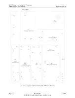
Page 118: ...FLO Technology Maintenance and Troubleshooting Exciter Maintenance Page 5 2 888 2604 001 03 08 07 WARNING Disconnect primary power prior to servicing 8439153013A PLT Figure 5 1 Top View of Exciter Ana...

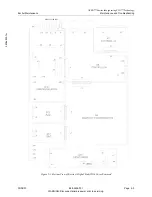
Page 119: ...nology Exciter Maintenance Maintenance and Troubleshooting 2604s500 fm 03 08 07 888 2604 001 Page 5 3 WARNING Disconnect primary power prior to servicing 8439153013B PLT Figure 5 2 Bottom View of Exci...

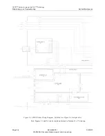
Page 120: ...hooting Exciter Maintenance Page 5 4 888 2604 001 03 08 07 WARNING Disconnect primary power prior to servicing Figure 5 3 APEX Exciter Wiring Diagram Left Side see Figure 5 4 for right side Note Figur...

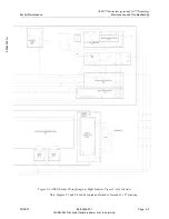
Page 121: ...e and Troubleshooting 2604s500 fm 03 08 07 888 2604 001 Page 5 5 WARNING Disconnect primary power prior to servicing Figure 5 4 APEX Exciter Wiring Diagram Right Side see Figure 5 3 for left side Note...

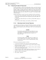
Page 122: ...caused by a faulty PLL board 5 1 2 1 Measuring Center Channel Frequency A special procedure which removes all transmitted data leaves only one center channel carrier This allows the channel center fr...

Page 123: ...rough 6 will contain written information When a successful connection is established use the left or right arrow key to access page 7 the blank page 8 Enter the following commands to turn off modulati...

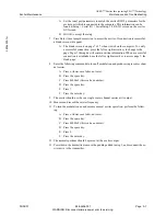
Page 124: ...ll take the exciter off the air A The output level should be 10 dBm 2 The 1st local oscillator frequency is affected by the 10 MHz reference oscillator A If the reference oscillator is off frequency t...

Page 125: ...ions provided with the software The serial port used for the software upgrade must be set up to use the Harris protocol See Section 3 6 6 1 Serial Setup Screen 1 of 3 RS 232 on page 3 45 for serial po...

Page 126: ...ne A UHF up converter tunable notch filter Values depend on UHF channel see Note 1 Tune B UHF up converter tunable B P filter RF IF Processing Screen 4 of 4 Section 3 4 5 4 1 Down Converter Diagnostic...

Page 127: ...tput if exciter is used to control transmitter output power RTAC Setup Section 3 6 3 RTAC Setup Screen on page 3 38 Filter Type Use FLO BANDPASS for this exciter Other Apex exciter application may use...

Page 128: ...xcessive MER Troubleshooting Flow Chart on page 5 15 Figure 5 5 Frequency Error Troubleshooting Flow Chart Is Exciter set to correct frequency Exciter Setup Screen N Y Set to correct frequency Frequen...

Page 129: ...ing Main Screen Power Control Power limit should be set higher than the required exciter output power See Setup Exciter screen 2 2 Y If power level at RF output of exciter is still low call technical...

Page 130: ...the Status Adaptive Processing screen normal See Figure 3 7 on page 3 9 N Y This screen shows the PA feedback sample level see Notes 2 Is this feedback sample out of range or Faulted Note 2 In Adaptiv...

Page 131: ...evels are correct Yellow average level and blue peak level Refer to Section 3 4 3 Adaptive Processing Board Status Screen on page 3 9 for additional information Y N If one or more diagnostic functions...

Page 132: ...it illuminates The screen saver may have been active Troubleshooting a dark screen is covered in Sec tion 5 8 2 on page 5 19 3 Are there any fault indications on the LCD display or front panel LEDs A...

Page 133: ...PA or driver If two successive amplifiers are both fairly non linear and especially if they have dif ferent non linearity curves correction at the output of the PA will be difficult if not impossible...

Page 134: ...O w RTAC Digital signal taken at output of adaptive precorrector board BIT Sample of the Built In Test FIFO for future use Exciter RF signal is taken from J4 sample output of exciter PA and connected...

Page 135: ...he 10 PLL Lock and the 10 kHz reference statuses will read N A since the 10 MHz oscillator is locked to the 1PPS signal via the FPGA modulator board the controller board and the PLL board DAC If a fau...

Page 136: ...power before the plastic shield is re moved from the analog tray The test meter is to be located outside the shield and the plastic shield replaced prior to applying power All of the power supply vol...

Page 137: ...board From there it goes to the DAC board the output of which is the 11 1 MHz first IF signal The first IF signal goes to the input of the up converter board in the analog tray 5 8 4 2 Analog Tray Si...

Page 138: ...viewing the analog loopback main screen On Air Data the SNR should be better then 32 dB and the LSB and USB lower and upper side bands should be better than 38 dB The chart source Post HPF Pre HPF an...

Page 139: ...in at amplifier connector J5 pin 7 unmuted 4 Vdc and muted 0 Vdc 5 8 6 Isolating a Faulty Board in the Digital Tray Isolating a faulty board in the digital tray involves checking the status screens of...

Page 140: ...roubleshooting defective ADC or DAC boards is covered in Section 5 8 5 1 Checking Operation of the Entire Digital Tray on page 5 21 5 8 6 4 Front Panel Board Troubleshooting a defective front panel bo...

Page 141: ...t of input and output signal levels Analog board frequency measurements are covered in Section 5 1 2 on page 5 6 Measure the PM noise of the CW signal outputs of the PLL board see Table 5 5 Phase Nois...

Page 142: ...Offset relative to CW signal Phase Noise PSD dBc Hz Frequency Offset relative to CW signal Phase Noise PSD dBc Hz 10 Hz 50 100 kHz 110 100 Hz 80 1 MHz 120 1 kHz 90 1 MHz 120 10 kHz 95 Table 5 6 Output...

Page 143: ...PF001 556 0170 000 ATTEN FIXED 5DB 2W SMA 3 EA AT001 AT002 AT003 610 1253 000 MALE CONNECTOR 4C 1 EA 628 0014 000 ADAPTOR SMA JACK TO BNC JACK 1 EA 646 0665 000 INSPECTION LABEL 1 EA 646 1487 000 NAME...

Page 144: ...PWA A D CONVERTER 1 EA A11 992 9995 013 PWA ADAPTIVE PRECORRECTOR 1 EA A9 992 9995 015 PWA UDC INTERFACE 1 EA A6 992 9995 030 PWA UPCONVERTER 1 EA A3 992 9995 033 PWA UHF BAND PASS FILTER 1 EA 992 99...

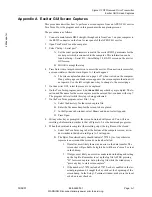
Page 145: ...r d but do not hit any other key as prompted The lo cation and file name for the screen capture must be entered first continue with step 7 The program will wait while this step is being performed 7 On...

Page 146: ...cing C Press the close soft key to close the log file 10 If you want to capture another screen after closing the log file select Control and then Reset terminal Press Enter twice and return to step 5...

Page 147: ...ond Drive Transmitter Exciter GUI Screen Captures 2604sapa fm 03 08 07 888 2482 001 Page A 3 WARNING Disconnect primary power prior to servicing Figure A 3 Tera Term Log Window Selected When Download...

Page 148: ...Sigma CD3 Diamond Drive Transmitter Exciter GUI Screen Captures Page A 4 888 2482 001 03 08 07 WARNING Disconnect primary power prior to servicing...

Reviews: