background image


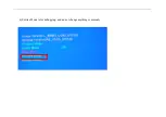
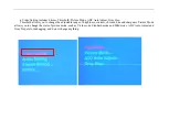
a. Video Setting includes 4 items, Threshold, Picture Mode, ADC Auto Adjust, Gray Step. 
Threshold allows you to change the adjustable range of brightness, contrast, chroma, hue and sharpness. Picture Mode 

allows you to change the state of picture mode, such as Vivid mode, Standard mode and Mild mode. ADC Auto Adjust and 
Gray Step are for debugging, and do not change anything. 


Summary of Contents for HL42B

Page 1: ...HL42B ...

Page 2: ...Safety Precautions 5 3 Images of Module and Circuit Boards 7 4 Key IC Description Trouble Shooting Guide 10 5 Signal Flowing Chart 14 6 Bus Control Adjustment 15 7 Circuit Diagram 30 8 Connection Sketch Interpretat 49 ...

Page 3: ...Scan yes Digital Comb Filter 3D Video Noise Reduction yes Picture Modes standard vivid mild custom of preset channels 181 Screen Mode 4 3 yes Wide Mode 16 9 yes Wide Mode PC yes Auto adjustment PC yes Phase PC Only yes Video Features H V edge correction yes Number Of Speakers 2 Speakers Type Built in bottom Speaker Size 4 1 2 X 2 2 pcs Watts Per Channel 10W Audio Audio Power Output 10W 2 Stereo Su...

Page 4: ...MI Input 2 Component Video Input 2 Composite Video Input 2 S Video Input 1 RF Input 1 PC Input 1 USB Port Analog Audio Input 2 for component 2 for composite and S video PC Audio Input 1 VGA and HDMI to DVI Audio Out Fixed Variable 1 optical Headphone jack 1 Input Output AV Output 1 Compliance Vesa N A Internal power Supply yes Power Consumption in Operation 240W Power Consumption in Standby 1W Pow...

Page 5: ...Safety Precautions ...

Page 6: ... ...

Page 7: ... Images of Module and Circuit Boards a Signal flow chart ...

Page 8: ... b Printed Circuit IC Board 1 head on board ...

Page 9: ... 2 rear board ...

Page 10: ... Key IC Description Trouble Shooting Guide 1 Key IC Description 1 BCM3551 ...

Page 11: ... 2 MSP3460 ...

Page 12: ... 3 AD9880 ...

Page 13: ... 2 Trouble Shooting Guide ...

Page 14: ... Signal Flowing Chart ...

Page 15: ...n And then press 9 4 4 3 OK in turn You will see the screen displaying as following You can check the version of the software adjust some settings But we don t advise you change this settings because of the TV has already hold in the state of optimality If you have to chang this settings please connect with the local service center 1 Factory menu ...

Page 16: ... 2 Image Version Atmega Version Image Version This is the current software version Atmega Version The serial number it is recorded for this board ...

Page 17: ... 3 OK MENU EXIT OK press OK to submenu MENU return to upper menu EXIT Press EXIT of the romote controller to exit from factory menu ...

Page 18: ...y Menu There are 5 items in the root Product Mode Aging Mode Shop End Service Mode Design Mode 1 Product Mode includes 3 items White Balance Setting Back Light Set to Factory Default Value Do not change the value commonly ...

Page 19: ... 2 Aging Mode This is for factory run in testing ...

Page 20: ... 3 Shop End is for debuging and do not change anything commonly ...

Page 21: ... 4 Service Mode is for debugging and do not change anything commonly ...

Page 22: ... 5 Design Mode includes 4 items Video Setting Audio Setting Screen Setting Others ...

Page 23: ...p Threshold allows you to change the adjustable range of brightness contrast chroma hue and sharpness Picture Mode allows you to change the state of picture mode such as Vivid mode Standard mode and Mild mode ADC Auto Adjust and Gray Step are for debugging and do not change anything ...

Page 24: ... b Audio Setting includes 4 items Sound Effect Sound Mode Sound Curve Headphone Sound curve All these items are for debugging and do not change anything commonly ...

Page 25: ... c Screen Setting allows you to change V SIZE V POSITION H SIZE H POSITION of the screen displaying Normally you need not to change anything ...

Page 26: ...Set E2prom to default will Clear all changing you have made to the TV set s software setting such as Channel list you have tuned volume brightness and etc and initialize TV set s software to the state like a new TV set buyed right now Remark The date of the chart only is a example please don t adjust the factory mode base on it ...

Page 27: ... 2 Others ...

Page 28: ... ...

Page 29: ... ...

Page 30: ... Circuit Diagram 1 BCM signal flowing chart 2 Circuit Diagram ...

Page 31: ...eo Audio Video 2 Composite Stereo Audio HD Component2 Stereo Audio Audio L R SD_CVBS EJTAG TestBSC FrontPanel Keypad LED IR HD Component1 Stereo Audio Audio L R Y Pb Pr HDMI1 HD_DVO RGB SD_L SD_C CVBS1 Luma1 ES_CVBS1 Broadband Studio Vision Probe BSC Masters control TPA3004D2 D AMP POWER NCP5422 12V 5V cpu 1 2v 2 6v 3 3v 5v Ethernet DTE Device USB Pb Pr Y Y Pb Pr DTT7608 ATSC NTSC Tuner RF Cable A...

Page 32: ...VI14 E18 HD_DVI 0 VI_656_0 B23 HD_DVI 1 VI_656_1 A23 HD_DVI 2 VI_656_2 D22 HD_DVI 3 VI_656_3 C22 HD_DVI 4 VI_656_4 E23 HD_DVI 5 VI_656_5 A25 HD_DVI 6 VI_656_6 D23 HD_DVI 7 VI_656_7 B24 HD_DVI 8 VI_656_8 F22 HD_DVI 9 VI_656_9 A24 HD_DVI 10 GPIO_62 C23 HD_DVI 11 GPIO_63 E22 HD_DVI_CLK_N D24 HD_DVI_CLK_P VI_656_CLK C24 HD_DVI_DE C25 HD_DVI_HSYNC G22 HD_DVI_VSYNC F23 Digital Video Input Compressed Aud...

Page 33: ...D1 FIDUCIAL MARK R422 2 2K R422 2 2K 1 1 TP30 tp_sq50 TP30 tp_sq50 R130 0_NC R130 0_NC R128 2 2K R128 2 2K C40 1uF C40 1uF R436 0 DNI R436 0 DNI 1 FD4 FIDUCIAL MARK FD4 FIDUCIAL MARK 1 1 TP31 tp_sq50 TP31 tp_sq50 C289 0 01uF DNI C289 0 01uF DNI 2 3 MH7 4 40X3 4in SCREW DNI MH7 4 40X3 4in SCREW DNI 1 FD5 FIDUCIAL MARK FD5 FIDUCIAL MARK L17 680nH 5 L17 680nH 5 L3 MPZ2012S221A L3 MPZ2012S221A USB_RRE...

Page 34: ...616 TDQU4 NC U616 TDQU4 NC FCT70 FCT70 R829 0 NC R829 0 NC R828 0 R828 0 BB 5V NC 1 TU 2 RF AGC 3 SCL 4 SDA 5 NC BTL 30V 6 5V 7 IF OUT 8 IF AGC 9 IF1 10 IF2 11 GND0 12 GND1 13 GND2 14 GND3 15 U614 ENV56M04D8F U614 ENV56M04D8F R417 0 R417 0 C507 0 01uF C507 0 01uF R831 0 NC R831 0 NC R832 0 R832 0 R343 100 R343 100 FCT71 FCT71 C513 2200pF C513 2200pF C505 0 01uF C505 0 01uF R377 0 R377 0 R347 10K_N...

Page 35: ...10 5 R189 10 5 C123 0 1uF C123 0 1uF C274 10uF NC 16V C274 10uF NC 16V L23 2 2uH L23 2 2uH R627 47K R627 47K A K D24 1N4148 D24 1N4148 D32 BAV99LT D32 BAV99LT C148 56pF 5 C148 56pF 5 FCT5 FCT5 C444 100pF C444 100pF R461 1 5M R461 1 5M R194 68 NC R194 68 NC 1 2 3 Q49 MMBT3904L Q49 MMBT3904L C272 0 47uF C272 0 47uF R634 100K R634 100K C413 100pF C413 100pF R224 0 R224 0 R628 47K R628 47K C522 0 47uF...

Page 36: ... B18 HDMI_DATA_1_P A18 HDMI_DATA_2_N C18 HDMI_DATA_2_P D18 HDMII_DDC_SCL A21 HDMII_DDC_SDA C20 HDMII_HTPLG_IN B20 HDMII_HTPLG_OUT A20 HDMI_RESREF F20 HDMI U22G BCM3551KPB5G BGA676_35X35 HDMI U22G BCM3551KPB5G BGA676_35X35 R477 4 7K R477 4 7K R617 100K R617 100K D912 BAV70LT D912 BAV70LT D65 ITC ESD0603 39V 0 8pF D65 ITC ESD0603 39V 0 8pF AUD_LEFT_N A13 AUD_LEFT_P B13 AUD_RIGHT_N B12 AUD_RIGHT_P A1...

Page 37: ...l area on the top layer of the PCB all the way to the connector MAIN_OUT R289 NC R289 NC R250 560 R250 560 R284 NC R284 NC C423 33uF C423 33uF 5 6 7 8 4 V V U35B LM358M SO8 V V U35B LM358M SO8 GPIO_40 HSYNC B16 GPIO_41 VSYNC A16 VDAC0_0 A14 VDAC0_1 C14 VDAC0_2 D14 VDAC0_3 B14 VDAC_RBIAS B15 Analog Video Outputs U22O BCM3551KPB5G BGA676_35X35 Analog Video Outputs U22O BCM3551KPB5G BGA676_35X35 R592...

Page 38: ... D10 DVO_3 E10 DVO_4 B9 DVO_5 C9 DVO_6 D9 DVO_7 A8 DVO_8 E9 DVO_9 F9 DVO_10 B8 DVO_11 C8 DVO_12 A7 DVO_13 D8 DVO_14 B7 DVO_15 E8 VO_656_0 DVO_16 C7 VO_656_1 DVO_17 A6 VO_656_2 DVO_18 G9 VO_656_3 DVO_19 D7 VO_656_4 DVO_20 F8 VO_656_5 DVO_21 A5 VO_656_6 DVO_22 C6 VO_656_7 DVO_23 E7 DVO_CLK_NEG B10 VO_656_CLK DVO_CLK_POS A10 DVO_HSYNC D11 DVO_VSYNC C11 DVO_DE A9 DVO_24 G7 DVO_25 D6 DVO_26 F7 DVO_27 A...

Page 39: ...0 10uF 16V C90 10uF 16V C442 220pF C442 220pF R637 1K R637 1K C156 100pF C156 100pF C779 0 1uF C779 0 1uF R601 100 NC R601 100 NC C770 56PF C770 56PF R598 27K R598 27K C764 0 1uF C764 0 1uF D88 BAV99LT NC D88 BAV99LT NC R591 470 NC R591 470 NC C440 0 1uF C440 0 1uF R577 15K R577 15K C782 NC C782 NC R281 0 R281 0 R587 470 NC R587 470 NC R817 100 R817 100 R273 15K R273 15K SCL 1 SDA 2 I2S_CLK 3 I2S_...

Page 40: ...ed if using SC_PRES for POD_EBI_WE1b function For DVB Common Interface card install R1312 and R1313 and remove R1301 R492 2 7K_NC R492 2 7K_NC R211 2 7K_NC R211 2 7K_NC R76 100 R76 100 R168 2 7K DNI R168 2 7K DNI VOUT 1 EN0 4 EN1 3 VOUT 8 5V 2 3V 7 3V 6 GND 5 U3 LTC1470CS8 NC SO8 U3 LTC1470CS8 NC SO8 R160 2 7K_NC R160 2 7K_NC R530 2 7K_NC R530 2 7K_NC R483 2 7K_NC R483 2 7K_NC R143 33_NC R143 33_N...

Page 41: ... 2006 POD1 POD2 BCM7411 USB Firewire Firewire ROM Test Test POD BCM7411 BCM7411 PROPRIETARY CONFIDENTIAL Connect PCI_VIO to 5V if any BCM3560 PCI or other digital pin is connected or pulled to a 5V source otherwise connect PCI_VIO to 3 3V Flash RESET Reset triggers when D3 3V 2 93V for 200ms Tri state CableCard POD bus to support hot insertion 1 2 3 4 5 6 7 8 RN22 4 7K RN22 4 7K C223 0 1uF C223 0 ...

Page 42: ...y 6 Place 22 ohm resistors for CLK ADDR BA DM RAS CAS WE CKE output only lines near BCM 7 Place DDR_VREF 2 1 resistor dividers near BCM 8 Trace impedances should be 60 to 65 ohms 9 Route DDR_VREF 2 1 with 30 mil trace and at least 1 high quality ceramic bypass capacitor for each connection to a device 10 All traces should have a 3 to 1 spacing ratio from the reference GND PWR layer e g 15 mil line...

Page 43: ...26 PLLTEST_MIPS AB8 VCXO27_A C26 VCXO27_B D25 CLOCKS U22B BCM3551KPB5G BGA676_35X35 CLOCKS U22B BCM3551KPB5G BGA676_35X35 C108 15pF C108 15pF R308 NC R308 NC R595 470 R595 470 C191 100uF NC 10V C191 100uF NC 10V R550 100 R550 100 R243 100 NC R243 100 NC 1 2 3 4 5 6 7 8 RN1 1K NC RN1 1K NC R551 100 R551 100 3 1 2 Q25 MMBT3904L Q25 MMBT3904L R622 2 7K R622 2 7K R532 2 7K DNI R532 2 7K DNI R191 0 R19...

Page 44: ...0uF C327 1000pF C327 1000pF FB34 BLM11A102S FB34 BLM11A102S R419 0 R419 0 C385 0 1uF C385 0 1uF C395 4 7uF C395 4 7uF R535 0 R535 0 C352 4 7uF C352 4 7uF C269 22uF 10V C269 22uF 10V C340 0 1uF C340 0 1uF FB31 BLM11A102S FB31 BLM11A102S C306 4 7uF C306 4 7uF C383 0 1uF C383 0 1uF C404 0 01uF C404 0 01uF C91 1000pF C91 1000pF C283 10uF C283 10uF C252 0 01uF C252 0 01uF C67 47uF 10V C67 47uF 10V FB23...

Page 45: ...3 U5 ISL6539CAZ U5 ISL6539CAZ L48 MPZ2012S221A L48 MPZ2012S221A C547 0 1uF NC C547 0 1uF NC D77 BAV99LT D77 BAV99LT R148 470 R148 470 C262 0 1uF C262 0 1uF L7 MPZ2012S221A L7 MPZ2012S221A L51 MPZ2012S221A NC L51 MPZ2012S221A NC 3 1 2 Q28 MMBT3904L_NC Q28 MMBT3904L_NC OUT 2 IN 3 GND 1 VO4 4 U23 LM1117SX ADJ U23 LM1117SX ADJ R14 0 R14 0 L115 47uH 250mA L115 47uH 250mA C235 0 1uF C235 0 1uF C44 10uF ...

Page 46: ...939 470uF 25V C939 470uF 25V R975 15K R975 15K R907 120K R907 120K C971 0 01uF C971 0 01uF R973 100K R973 100K D89 BAV99LT D89 BAV99LT C983 0 1uF C983 0 1uF 1 1 2 2 3 3 4 4 5 5 6 6 7 7 8 8 9 9 J904 CKX3 3 5 02AC J904 CKX3 3 5 02AC C567 0 47uF C567 0 47uF A K D94 1N4148 NC D94 1N4148 NC D91 1N4148 D91 1N4148 C969 0 1uF C969 0 1uF C940 1000pF C940 1000pF C560 0 47uF C560 0 47uF FCT78 FCT78 C171 47uF...

Page 47: ...0K DNI R22 10K DNI IN 3 GND 1 OUT 2 H S OUT 4 U17 LM1117MPX 1 8 SOT223 U17 LM1117MPX 1 8 SOT223 C34 0 1uF C34 0 1uF C438 0 1uF C438 0 1uF TP3 TP3 C435 0 1uF C435 0 1uF FB21 BLM11A102S FB21 BLM11A102S C271 0 1uF C271 0 1uF C409 0 47uF C409 0 47uF TP2 TP2 C432 10uF 6 3V C432 10uF 6 3V R646 2 7K R646 2 7K C53 0 01uF C53 0 01uF C43 33uF 6 3V C43 33uF 6 3V C437 4 7uF C437 4 7uF C422 4 7uF 6 3V C422 4 7...

Page 48: ...006 Title Size Document Number Rev Date Sheet of Doc 05 Hudson LCD TV A 18 18 Tuesday November 07 2006 FCT65 FCT65 C198 0 1uF C198 0 1uF FCT82 FCT82 R963 1K R963 1K C94 470uF 25V C94 470uF 25V C124 470uF 35V C124 470uF 35V 1 2 D909 SK34 D909 SK34 FCT80 FCT80 L128 33uH 3A L128 33uH 3A C142 1000pF C142 1000pF FCT81 FCT81 1 2 3 4 5 XS12 PH 5A XS12 PH 5A VIN 1 OUT 2 GND 3 FB 4 EN 5 TAB 6 U19 LM2596S A...

Page 49: ... Connection Sketch Interpretat ...

Reviews: