GV-395 Virtex-II DSP Hardware Accelerator Manual
GV & Associates, Inc.
07/10/04
4
1.0
GVA-395 Introduction and General Description
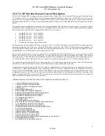
The GVA-395 Modular DSP Development Platform consists of three Xilinx FPGAs. Two Virtex-II FPGAs are used for Analog Control
(ACX and AC) and two Virtex-II FPGAs are used for Data Processing (DP and DPX) respectively. The DPX FPGA also serves as the
primary FPGA for external communication. A Spartan-II FPGA (EI) is used for interfacing to provide a 5V tolerant external interface.
An additional Spartan-II FPGA is used to assist in programming the bit stream into the Flash EPROM and the configuration of the other
FPGAs.
The platform’s general configuration consists of 12 interchangeable daughter PCBs that allow for a wide range of I/O capability. Eight of
the daughter PCBs are dedicated to the ACX FPGA. Two daughter PCBs are dedicated to the AC FPGA and an additional two daughter
PCBs are dedicated to the DP FPGA. Daughter PCB modules are to be as follows:
•
100 MSPS 12 bit A/D (GVA-AD9432)
•
170 MSPS 12 bit A/D (GVA-AD9430)
•
100 MSPS 14 bit A/D (GVA-AD6645)
•
100 MSPS 12 bit D/A (GVA-AD9762)
•
160 MSPS 14 bit D/A (GVA-AD9772)
•
Customer specific designs may be implemented.
The digitized data from the daughter PCB may be processed by the ACX FPGA and passed to the other FPGPs for further processing.
The processed data may also be sent to the external LVDS data port via the DPX Virtex-II FPGA. A data file may also be uploaded via a
USB or Parallel Port interface and may be imported into MatLab for additional analysis. A data file may also be downloaded to the on-
board SDRAM via two USBs interface for processing by the GVA-395.
The ACX and AC FPGAs have access to an external
256K x 18 ZBT SRAM, the DP FPGAS has access to an external 1M x 18 ZBT
SRAM, and the DPX has access to four external 1M x 18 ZBT SRAMs that can be used for temporary data storage. Each Virtex-II
FPGA also has up to 1,728,000 bits of internal Block SelectRAM. There individual 100 bit dedicated local buses connecting the ACX,
AC, DP and the DPX FPGAs. Additionally, there is a shared 43 bit local buses between the ACX, AC, DP, DPX and the EI FPGAs.
The external interface Spartan II FPGA (EI) is used to provide a +5V CMOS tolerant interface between the Virtex-II FPGAs and other
external devices. However, this FPGA could be used for additional processing as determined by the user.
Using the 48-bit external bus interface, the GVA-395 could be configured to have an off-board interface to an external processor such as
a TMS320C31 or other Digital Signal Processors. Additionally, the GVA-395 can be configured either by the Multilinx JTAG cable or
by the on-board FLASH EPROM. The on-board FLASH EPROM can be programmed through the use of the Multilinx Slave Serial
configuration connector. The Xilinx FPGAs may also access unused address space in the configuration EPROM by interfacing to the
Spartan-II configuration FPGA via either the FPGA local bus or the dedicated 32 bit Spartan-II external interface bus. For non-specific
clock requirements, an external clock source is available.
Additional features are listed below and will be explained in detail in Section 2.0.
•
4 Virtex™-II FPGAs for Signal Processing
•
1 Spartan™-II FPGA for External Interface
•
1 Spartan™-II FPGA for Configuration Control
•
3 USB interfaces
•
Supports Xilinx ChipScope-ILA
•
12 Interchangable I/O Daughter PCB capability
•
Dedicated external communication FPGA for analog control
•
Eight Digital Clock Managers per Virtex-II FPGA
•
Up to 168 18x18 Multipliers per Virtex-II FPGA
•
+5 V tolerant 48 bit external I/O
•
32 Bit LVDS interface
•
FPGA logic expansion (1.5M to 3M gates)
•
Each Virtex-II FPGA has at least a dedicated 256K x 18 ZBT SRAM
•
Up to 3,024,000 bits of internal Block SelectRAM™
•
100 bit local bus between the each of Virtex-II FPGAs
•
43 bit shared local bus between Virtex-II and Spartan-II FPGAs
•
JTAG download configurable
•
On-board 16M x 8 FLASH EPROM
•
On-board FLASH EPROM programming
•
On-board 20 Amp 1.5V Core Power supply
•
Programmable A/D and D/A sample clocks
•
On-board 50 MHz clock oscillator (which can be doubled by the Virtex-II DLL).
•
External high stability clock Input
•
Four bit DIP Switch for internal use by FPGAs


